The design, simulation, realization, and measurement of an ultra-wideband (UWB) antenna on a polymeric substrate have been realized. The UWB antenna was prepared using conventional technology, such as copper etching; inkjet printing, which is regarded as a modern and progressive nano-technology; and polymer thick-film technology in the context of screen-printing technology. The thick-film technology-based UWB antenna has a bandwidth of 3.8 GHz, with a central frequency of 9 GHz, and a frequency range of 6.6 to 10.4 GHz. In addition to a comparison of the technologies described, the results show that the mesh of the screens has a significant impact on the quality of the UWB antenna when utilizing polymeric screen-printing pastes.
1. Introduction
Ultra-wideband is a comprehensive term that refers to short-range wireless technology that consumes low power and transmits data over a wide bandwidth (more than 500 MHz or with a relative bandwidth greater than 20%) in the frequency range of 3.1 to 10.6 GHz
[1]. A high transmission rate can be achieved by combining a large bandwidth covering the majority of the radio spectrum with an appropriate modulation (such as Pulse Position Modulation (PPM), Pulse Amplitude Modulation (PAM), Bi-Phase Modulation (BPSK), Code Division Multiple Access (CDMA), or Orthogonal Frequency Division Multiplexing (OFDM))
[2]. UWB technology has a wide range of applications, including data transmission and sensor data collecting in modern networks, such as WPAN (Wireless Personal Area Networks) for interconnecting electronic devices
[2] and WBAN (Wireless Body Area Networks) for continuous health monitoring
[3]. Additionally, it can be utilized to locate or detect moving objects, such as in collision avoidance systems or human sensing.
Patch antennas are a common type of UWB antenna. Circular, elliptical, triangular, rectangular, or polygonal are the most basic shapes of patch antennas
[4]. However, the variety of patch antenna topologies is enormous at the moment and far from being limited to these fundamental designs. Patch antennas are frequently taking on more complicated shapes and even fractal patterns in order to increase their parameters and efficiency
[5][6]. Various structures, such as the Defected Ground Structure (DGS), can also be used to improve the parameters of antennas
[7]. The antenna’s impedance matching with the feed line, which is frequently a microstrip, is a significant parameter. Advanced methods such as the Genetic Algorithm (GA), Particle Swarm Optimization (PSO), and Differential Evolution (DE) can also be utilized to optimize the topology of patch antennas and antenna arrays
[8][9]. As a result, contemporary design processes are intimately connected to Computer-Aided Design (CAD), simulation, and computational tools. However, even with the best design, simulation, and optimization techniques, if the limitations of the manufacturing technology are not considered, the output is frequently worthless.
Certain applications, such as WBAN, depend on wearable UWB antennas to function
[10]. There are numerous technologies available for producing UWB antennas in terms of wearable electronics. For example, a non-conductive fabric (jeans, fleece, felt, plain-woven polyester fabric, etc.) can be utilized to fabricate a wearable antenna with a radiating component made of conductive materials, such as copper foil
[11][12] or another conductive fiber
[13][14]. Even wearable antennas made from various conductive threads have been investigated, whether they are made of electroconductive polyester yarn covered in Cu–Ni alloy
[15] or a silver-plated nylon thread
[16]. For antennas on flexible substrates, and particularly for wearable antennas, it is necessary to take into account the effect of bending or crumpling the substrate with the patch antenna on the resulting parameters, such as the antenna resonant frequency, scattered parameters, radiation pattern, and S
11 parameter
[17][18][19], as well as the mechanical properties of the substrate, especially for wearable antennas
[20].
32. Influence of Various Technologies on the Quality of Ultra-Wideband Antenna on a Polymeric Substrate
The reflection or scattering parameter S
11 was evaluated as a quality factor for the designed, manufactured, and measured UWB antenna. The red line represents the simulated reflection coefficient of the designed UWB antenna and acts as a reference curve in all graphs in this section. According to the simulation results, the designed antenna has a BW of 3.2 GHz, ranging from 7.35 GHz to 10.55 GHz. The reflection coefficient was measured using the Agilent N5241A PNA network analyzer. SMA connectors were used to connect the measurement cable to the antenna, which was conductively bonded to the antenna using the epoxy-based conductive glue NCNR 8331.
In
Figure 1, the impact of the mesh of the used screens on the UWB antenna’s reflection coefficient is illustrated using the screen-printing paste XZ250. The worst results were obtained with 200 mesh due to the lowest attenuation. The best results in terms of resonance frequency and high attenuation were obtained when 325 mesh was used. The 400 mesh showed a significant shift in resonance frequency. Although the resonant frequency has been slightly moved to 9.15 GHz, the reflection coefficient is nearly identical to that of the simulated curve. The observed improvement in the measured S
11 parameter was achieved when the mesh was increased from 200 to 325. According to the datasheet for the examined paste, the manufacturer recommends mesh sizes ranging from 124 to 228 (49–90 T/cm), which is much less than the mesh sizes used in the experiments. A smaller mesh size limits the creation of precise structures, but it is ideal for printing pastes with a higher viscosity and larger particles. Although a larger mesh is better for printing accurate structures, strict requirements for the rheological properties of the applied pastes exist. However, it has been demonstrated that this paste is suited for higher meshes, with results demonstrating that it is applicable up to 325 mesh and increases the quality of printed structures.
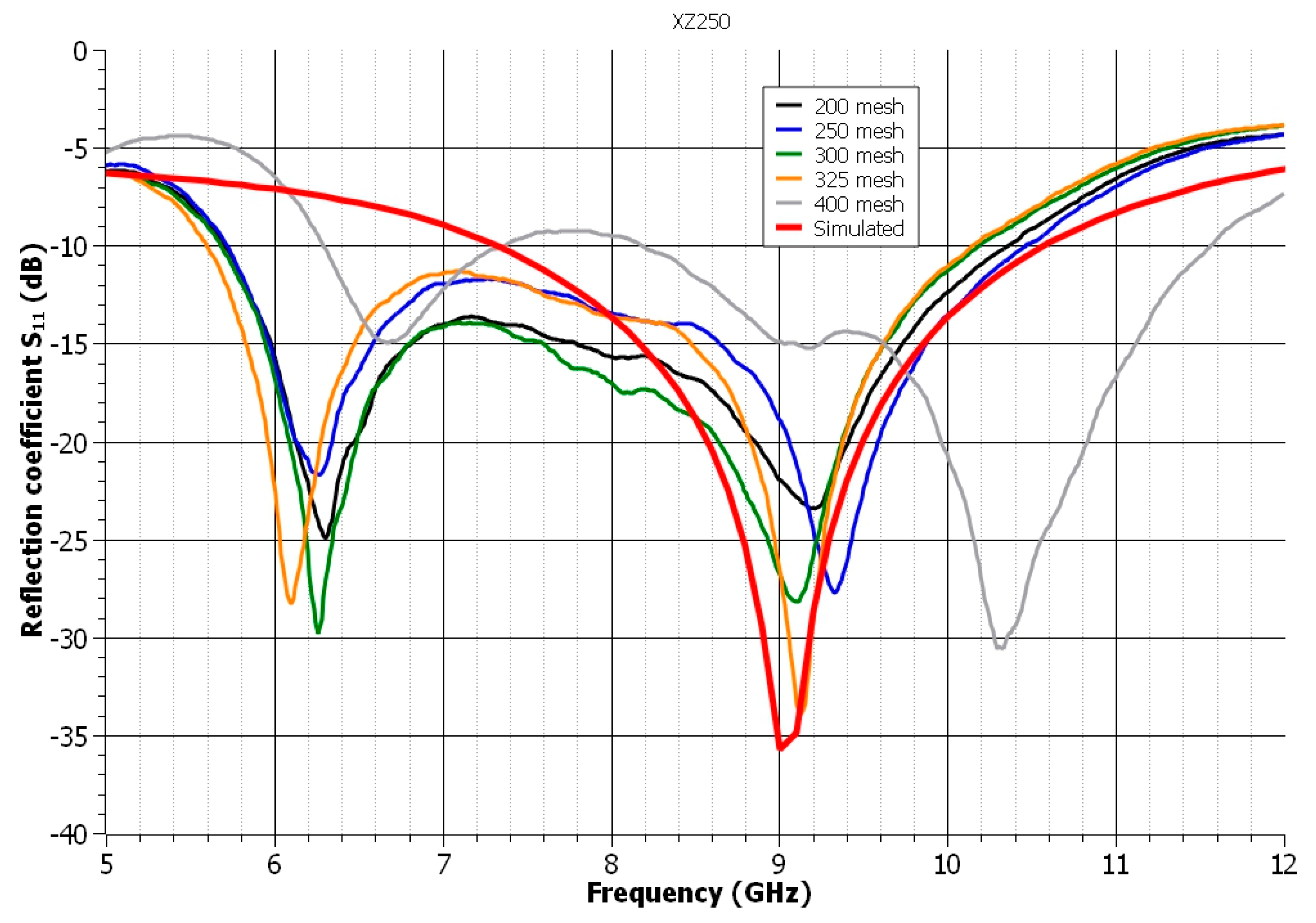
Figure 1. The influence of the mesh of the used screens on the reflection coefficient of the antenna—paste XZ250.
Plasma discharge treatment of the surface increases the surface free energy
[21]. This leads to a change in the wettability of the polymeric substrates’ surfaces, which results in the spread of the screen-printing paste during the deposition process. As illustrated in
Figure 2, the dimensions of the UWB antenna’s radiating and feeding element varied, resulting in an uncontrolled increase in the antenna’s resonant frequency. On the other hand, plasma treatment contributes to the smoothing of the printed structure’s edges.
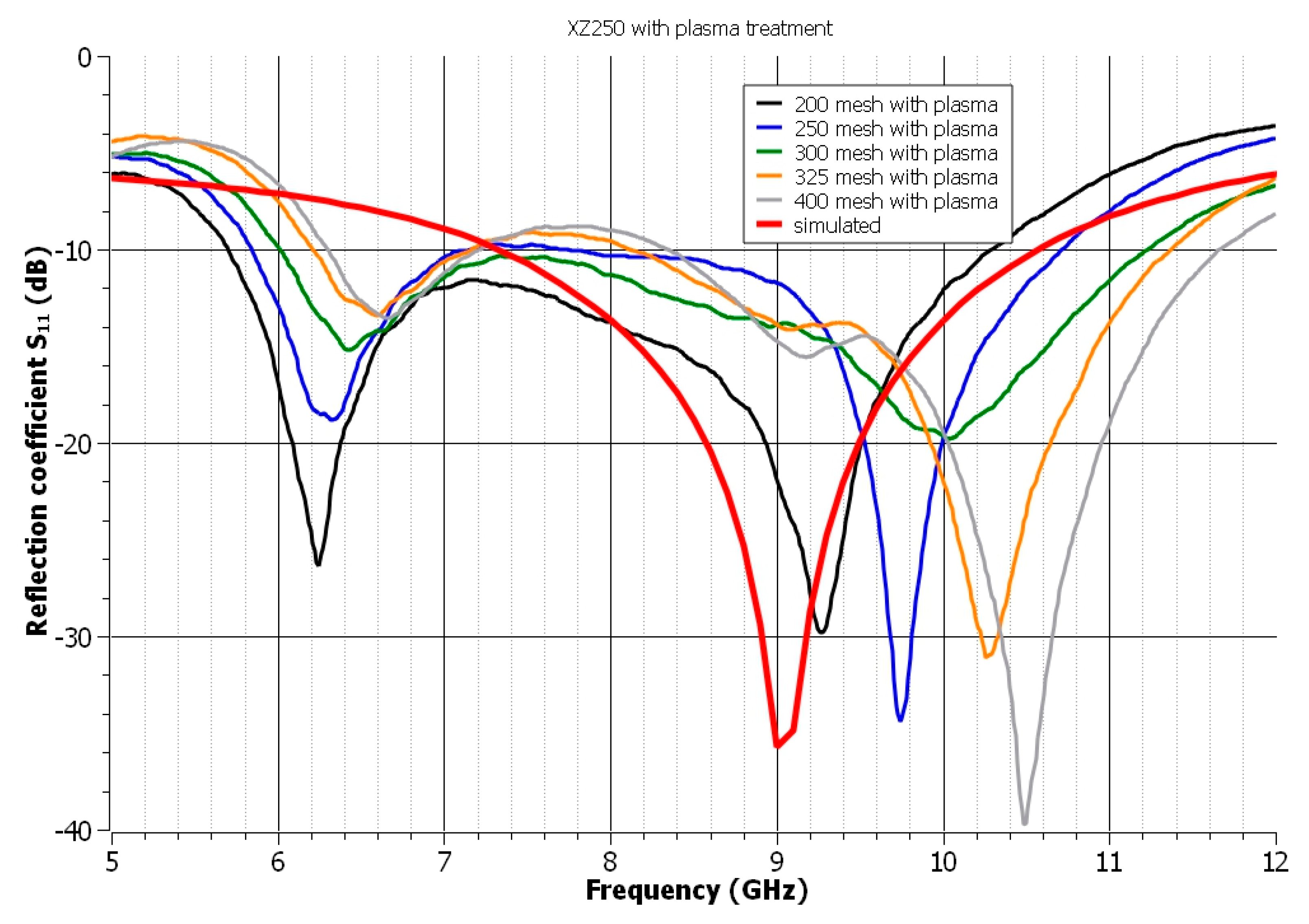
Figure 2. The influence of the mesh of the used screens on the reflection coefficient of the antenna after the plasma treatment—paste XZ250.
In the case of the second analyzed polymeric paste, ED3000, the best result was obtained when a screen with a mesh size of 400 was used. The realized antenna’s bandwidth was increased to 3.8 GHz from 6.6 to 10.4 GHz. On the other hand, as illustrated in
Figure 3, the mesh of the used screens had the biggest impact on the antenna’s reflection coefficient. Meshes 200 and 250 cause the shift in the resonance frequency and an insufficient reflection coefficient. Meshes of up to 300 cause the UWB antenna’s resonant frequency to stabilize and the reflection coefficient to decrease in accordance with the simulated curve. The manufacturer recommends a mesh size range of 200 to 325 for stainless steel screens. The results demonstrate that increasing the mesh size also improves the quality of the printed structure in this context.
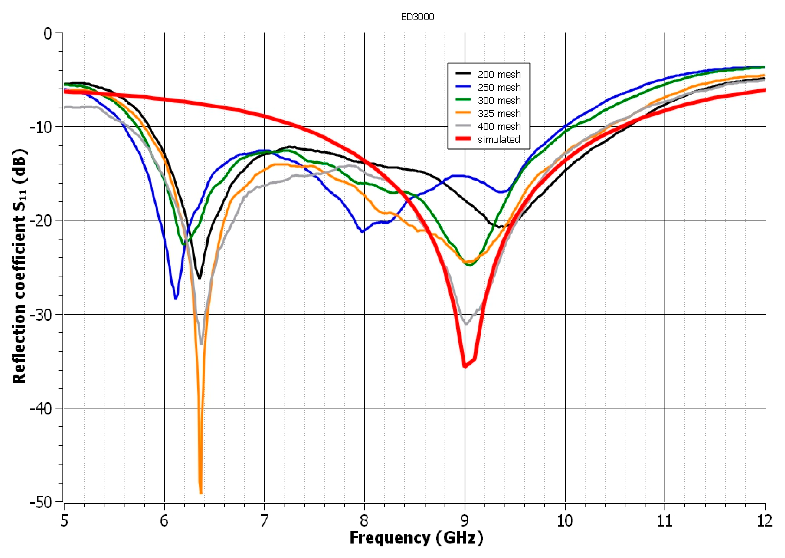

Figure 3. The influence of the mesh of the used screens on the reflection coefficient of antenna—paste ED3000.
Plasma treatment of the polymeric paste ED3000 has the same effect as it does with the paste XZ250, essentially changing the resonance frequency of the UWB antenna (
Figure 4). As illustrated in
Figure 5, when the screen with 200 mesh was plasma-treated, an electrical short occurred.
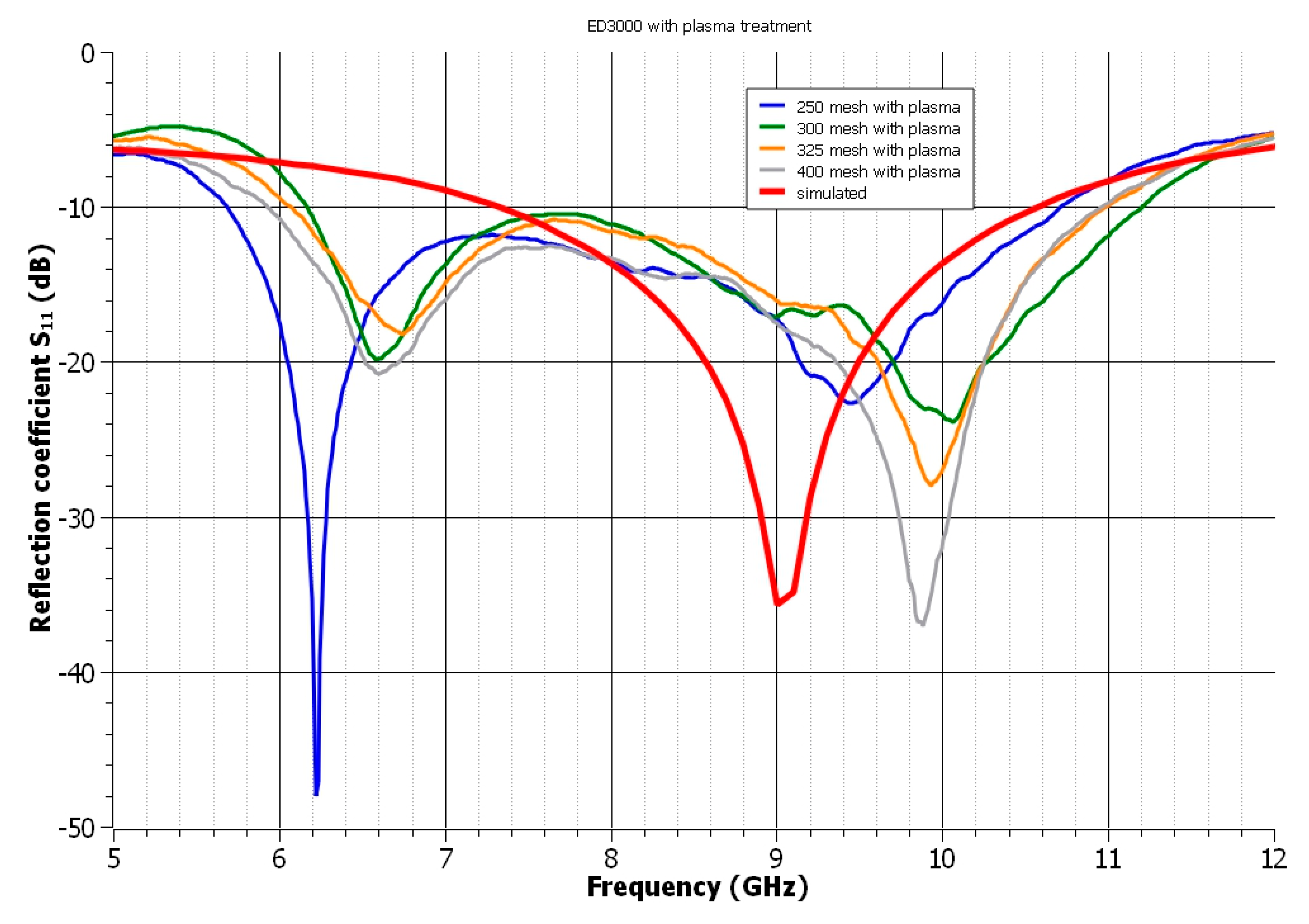
Figure 4. The influence of the mesh of the used screens on the reflection coefficient of the antenna after the plasma treatment—paste ED3000.
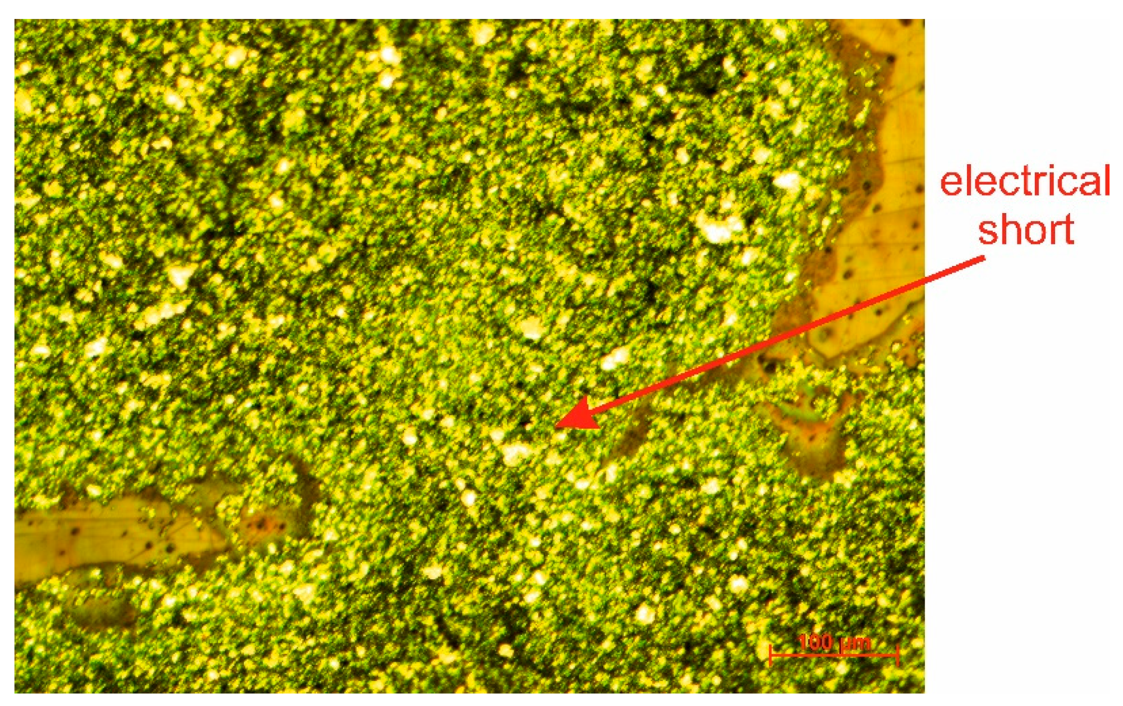
Figure 5. Electrical short caused by the plasma treatment in the case of the paste ED3000 (200 mesh).
The future of graphene-based materials is bright due to their beneficial properties and, most importantly, their ecological origin. Graphene is an organic material, and its use in combination with polymeric insulators enables green electronics
[22][23]. Graphene has a lower conductivity than printed metallic inks or pastes based on silver particles, which is the most frequently used conductor material in the fabrication of flexible antennas
[24]. Nevertheless, graphene-based structures have a number of advantages, including chemical and mechanical stability, low cost, fatigue resistance, stability in harsh environments, and bending resilience, making them an ideal candidate for flexible antennas
[25]. The behavior of graphene compared to silver is significantly different. Graphene is a semi-metal with no band gap and extremely high carrier mobilities (up to 200,000 cm
2V
−1s
−1) due to its unique two-dimensional honeycomb lattice
[26][27], in comparison to silver (which forms the basic conductive component of the remaining screen-printing pastes), which is a metal with a typical band structure and carrier mobility of 50 cm
2V
−1s
−1 at room temperature
[28]. There is also a frequency dependence in graphene’s surface conductivity, but this is more evident at THz frequencies
[26], which has not been investigated
in the paper because of the UWB’s definition by FCC. As a result, the antenna was also realized using Electra’s screen-printing paste ED5020. The ED5020 screen-printing paste is developed for use on rigid substrates. Due to the difference in thermal expansion coefficients (TEC) between the paste and the polyimide substrate, only samples printed through the 400 mesh screen were investigated. As illustrated in
Figure 6, the BW of the realized antenna is greater than that of the simulation. The BW is 4.42 GHz from 5 to 9.42 GHz before plasma treatment. After plasma treatment, the BW is 5.45 GHz, ranging from 5.5 to 10.95 GHz. The application of the plasma treatment results in an increase in the resonant frequency. As demonstrated in
Figure 6, graphene-based materials are the most suitable alternative to conventional etching technologies. It is critical to keep in mind that by applying the plasma treatment, the screen-printing paste that is typically used on rigid substrates can also be used on flexible substrates.
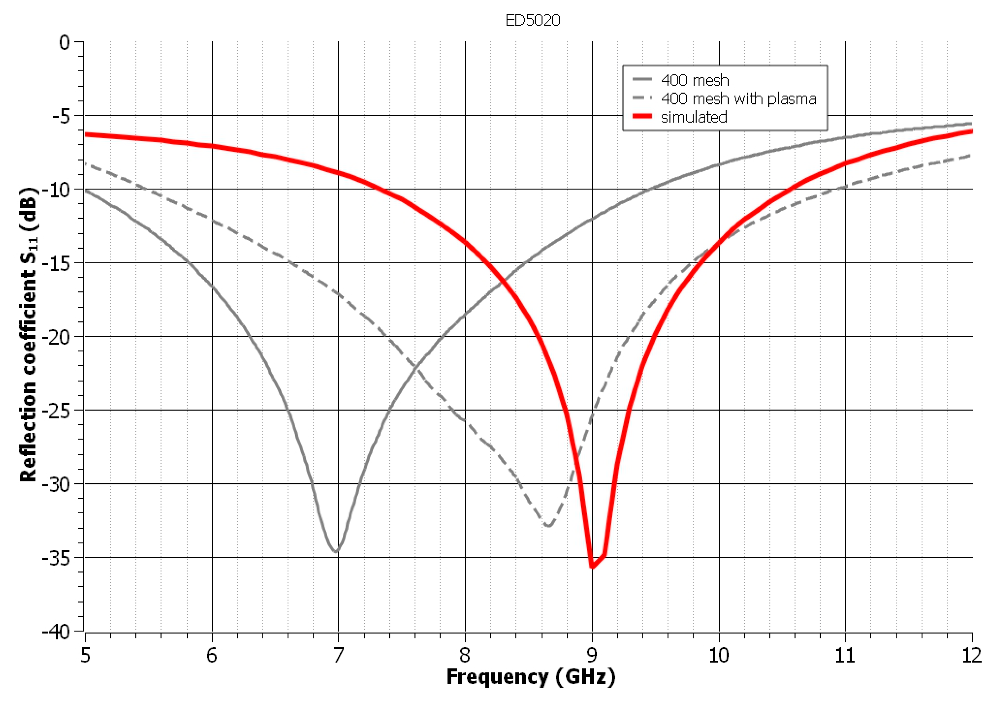
Figure 6. The influence of the mesh of the used screens on the reflection coefficient of the antenna—carbon-based paste ED5020.
By removing organic contaminants from the surface and attaching oxygen-containing molecules to it, the plasma treatment aims to convert a low-energy surface to a high-energy surface
[29][30]. This results in the increased wettability of polymeric substrates and the spreadability of screen-printing pastes. If the paste spreads more widely on the surface, the radiation area becomes larger, and the feeding element becomes wider. As a result, the antenna’s resonance frequency and bandwidth are modified. Plasma treatment leads to a change in the resonant frequency and an increase in the bandwidth of the realized UWB antenna in each investigated screen-printing paste.
The reflection coefficient of the materials chosen to provide the best solutions is illustrated in
Figure 7. As is obvious, the inkjet-printed UWB antenna has the highest reflection coefficient. It is necessary to keep in mind that the principle of inkjet printing technology is based on a drop-by-drop system, which results in the printed structure’s regular edges
[31], as illustrated in
Figure 8. Smooth or regular edges are critical in the HF area due to the uniform wave reflection. Additionally, inkjet printing technology allows precise printing. This technology’s combination of these two advantages makes it the most suitable for the realization of UWB antennas
[32][33]. Despite the shift in resonance frequency, graphene-based materials also provide an attractive solution for the implementation of UWB antennas due to their wide BW. However, in the case of the paste ED5020, it is critical to match the design to the paste’s low spreading characteristics or plasma treat the polymeric substrate’s surfaces. Both polymer-based screen-printing pastes containing silver particles are appropriate for realizing UWB antennas; nevertheless, it is imperative to analyze the effect of the screen mesh on the final quality of the UWB antenna. Polyimide substrates coated with a copper layer, called Pyralux, provide consistent quality in high-frequency applications. From a green electronics standpoint, this method is the least acceptable because of the hazardous wastes.
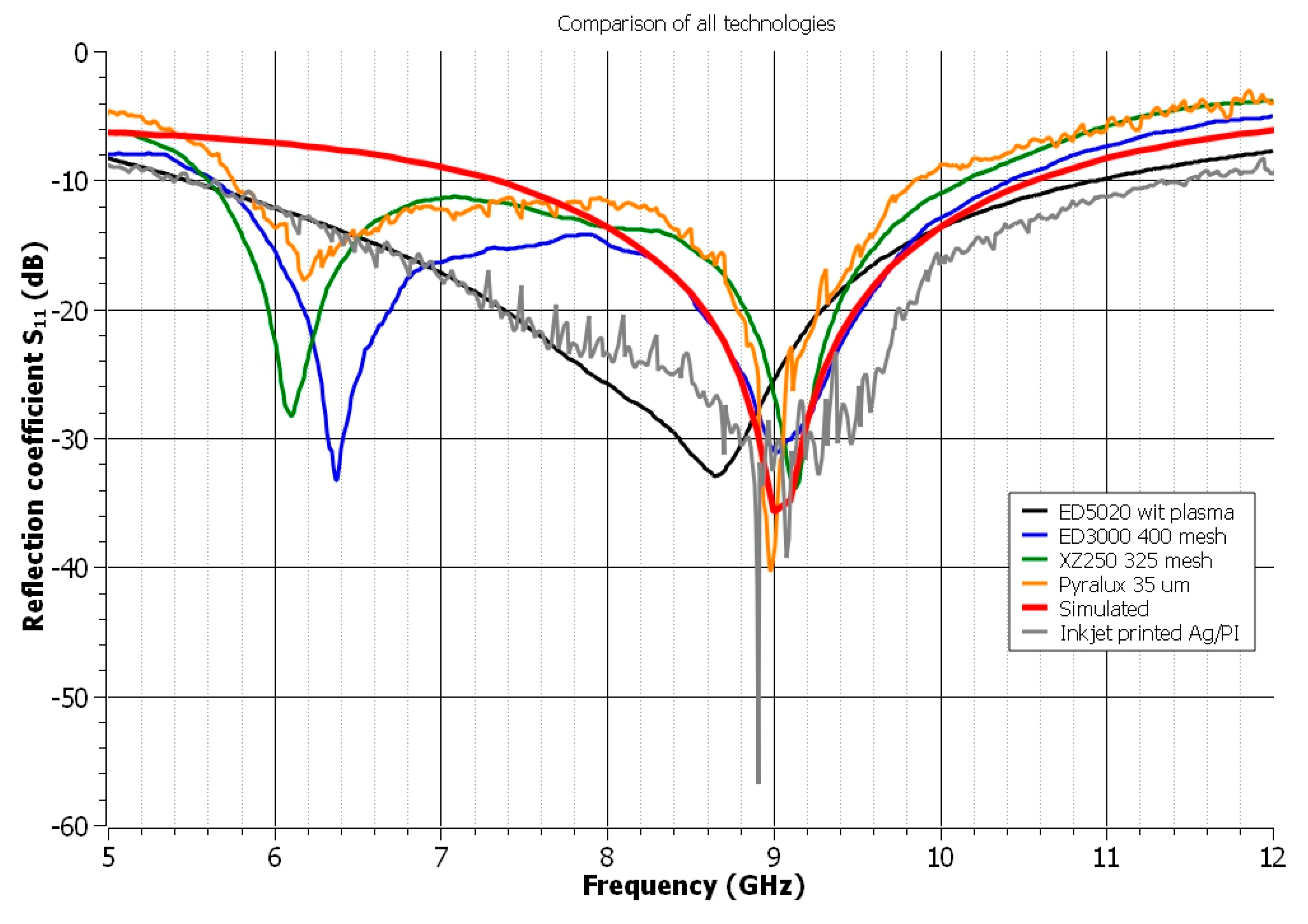
Figure 7. The reflection coefficient of all analyzed materials—selection of the best solutions.
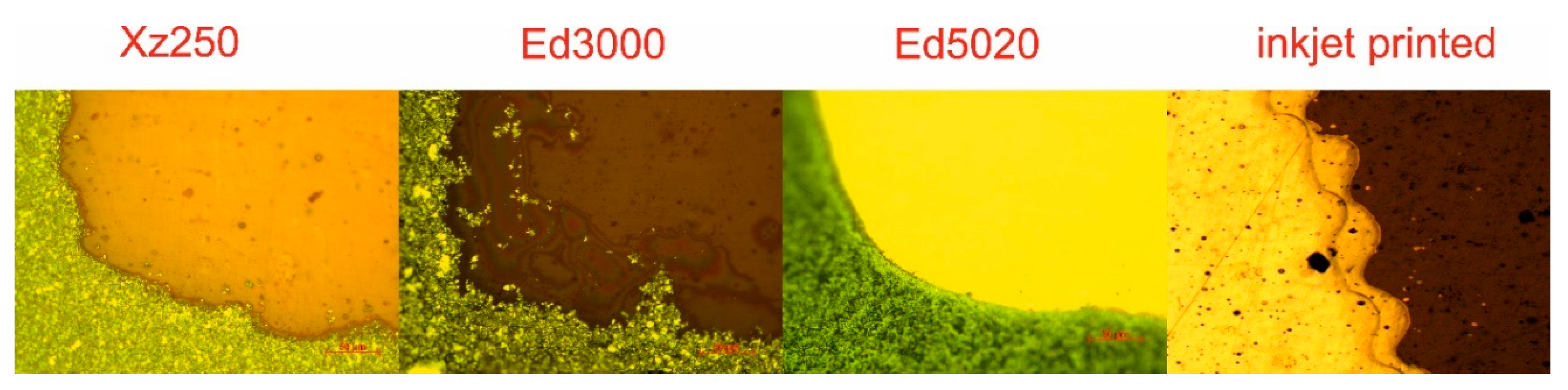
Figure 8. The edges of the realized UWB antenna by screen-printing with the 400 mesh and inkjet-printing technology.
The antennas were fabricated using a variety of conductive materials (the silver-based pastes XZ250 and ED3000, as well as the nano-ink JP-6n, the graphene-based screen-printing paste ED5020, and polyimide film coated with copper—Pyralux). The conductivity of the materials used had no effect on the scattering parameter of the UWB antenna. As a consequence, this influence was not investigated
here.
The simulation was performed on a 50 µm-thick polyimide substrate with a dielectric constant of 3.4 and a homogenous conductive layer. It is important to keep in mind that the experiments compare three different manufacturing technologies, two of which are based on particle sintering or curing, which results in an inhomogeneous structure. The process of the sintering of particles lies in a connection of particles by necks into the conductive structure, whereas the final structure consists of the conductive necks and polymeric material of which the cavities around the necks are filled
[34]. This polymeric material and its particle dispersion have a direct effect on how the transmitted signal scatters
[22]. The behavior of the electronics structure (antenna, filter, etc.) varies depending on the sintering conditions of the particles obtained in pastes
[35]. Additionally, screen-printing technology entails the development of the exposure mask, screen, and printing process. All of these factors lead to imperfections, and the designed structure will probably differ slightly from the realized structure. As a result, in some circumstances, the measured bandwidth of the reflection coefficients matches well with the simulation. However, except for the material ED5020, the measured antennas’ resonance frequencies match the simulation. The resonance frequency is 300 MHz lower in this case.
The homogeneity, thickness, and roughness of the layers do influence the signal transmission loss and, in this case, the UWB antenna’s reflection coefficient
[36][37][38]. T
he results presented here proved the effect of these parameters on the antenna behavior. The lower thickness of the printed layers is achieved by increasing the mesh size of the screen-printing pastes used, which offers a predisposition to precise edges in critical areas of the antenna. On the other hand, the thinner conductive layer more closely replicates the surface of the polymeric substrate, resulting in inhomogeneity. During the deposition process, plasma treatment has an effect on the surface properties of the substrates. In both cases, depending on the mesh, the resonance frequency of the UWB antenna was shifted up to the higher frequency using the polymeric pastes XZ250 and ED3000.
As stated previously, the edges of the realized structure are critical in HF applications. As a consequence,
Figure 8 shows microscopic views of the critical part of the UWB antenna. In a comparison of screen-printed polymeric pastes, the polymeric paste XZ250 achieved the smoothest edges. The more disheveled edges were obtained with the ED3000 paste. Uneven edges can operate as a source of radiation and affect the final quality of the UWB antenna. A partial solution to this problem is to apply plasma treatment to the surfaces of polymeric substrates. Plasma treatment smooths the edges and partially eliminates the irregularities. On the other hand, plasma treatment causes the screen-printing pastes to spread more widely. The most refined edges were obtained with the carbon-based paste ED5020. The results demonstrate the potential of polymeric and graphene-based materials for the fabrication of UWB antennas.
The viscosity of all used pastes was measured as one of the rheology parameters using a HAAKE PK-100 with the measuring system M5 (maximum torque 4.9 Ncm, speed range 0.05 to 500 rpm) to support the understanding of screen-printed sample results. Rotovisco RV 20 and programmer PG 242 were used to ensure operation controls during the measurement, and an oil system HAAKE C with a regulator HAAKE F3 was used to regulate the temperature. A cone and plate system with a cone angle of 1° was used. Before the screen printing, the viscosity of the ED3000 and XZ250 pastes was not modified, however, the viscosity of the ED5020 paste was decreased using the Electrareducer ER7. The viscosities of all thick-film pastes used for screen printing at 25 °C, and three different shear rates (D = 30 s
−1, 150 s
−1, and 300 s
−1).
The measurements clearly show that the pastes had significantly varied viscosities. The waviness of the printed antenna’s edges (
Figure 8) is the smallest for the highest viscosity paste (ED5020), and the shape of the pattern in the screen can be reproduced more precisely. In comparison, the printed edges of the pastes with a lower viscosity (XZ250 and ED3000) had a low quality. Together with the plasma treatment, which resulted in increased paste spreading, there was a more obvious change in antenna dimension and, as a result, in the final antenna parameters when compared to the simulation. As a result of this, it can be concluded that better results were obtained with ED5020 paste due to its rheological properties and better reproduction of the designed antenna’s dimensions.