Your browser does not fully support modern features. Please upgrade for a smoother experience.
Please note this is a comparison between Version 2 by Rita Xu and Version 3 by Lindsay Dong.
Computing systems are widely used in medical diagnosis, climate prediction, self-driving cars, and more. This entry mainly introduces the Chiplet-based computing system architecture design technology, which can solve the conflict between performance, efficiency and cost in computing system design, and provide instructions for the design of a high-performance computing system.
- computing system
- computing architecture
- memory architecture
1. Introduction
Electronic equipment is becoming more intellectualized with the development of 5G, artificial intelligence (AI), and big data. It has been widely used in medical diagnosis, automotive, electronic product design, Industry 4.0 Internet of things, etc. In the medical field, computer-aided diagnosis can improve efficiency and accuracy by preprocessing and classifying pathological images [1]. Explosive data from vehicles sensors and high-precision avigraph are also processed by computing systems for safety [2]. In addition, computing systems have been used to analyze data from the Internet of Things (IoT) to improve efficiency in smart factories [3]. Precision equipment can be designed by using a computing system; therefore, high-performance computing systems are crucial in electronic equipment [4].
Traditionally, the performance of computing systems can be improved by increasing transistors and frequency of integrated circuits (IC) [5]. In order to meet the requirements of the higher computing power, energy efficiency, and the lower cost of diversified applications, architectural innovation and technology scaling have been proposed to achieve these goals. The computing systems have been developed from single-core to multi-core, including homogenous multi-core and heterogeneous multi-core. In the data-centered applications, the traditional approach is facing some problems: (1) explosive costs [6]; (2) rapid increase in leakage power; (3) scalability degrades; (4) system design complexity increases, which can affect the improvement of the computing system. Due to the advantages of Chiplet, it has been used in the architecture of computing systems [7][8]. Chiplet is a small-scale hard IP with high yield and reusability [9][10][11]. The computing system architecture design based on Chiplet glues together the advantages of technology scaling, three dimensions (3D) integration technology, and a new device to construct a high-performance computing system, which has some merits (1) reducing the design cost via a smaller area and higher yield [12]; (2) avoiding the dark silicon effect [13]; (3) shortening the design cycle by Chiplet reuse; (4) improving the system scalability by flexible Chiplet combinations [14].
The appropriate computing system architecture can effectively utilize the advantages of Chiplet technology in specific applications. This entry mainly introduces the computing system architectures based on Chiplet, as shown in Figure 1, which mainly includes computing architectures and memory architectures. In computing architecture, 2.5D and 3D computing architectures based on Chiplet are presented and compared. In-memory architecture, near-processor memory architecture, and processing-in-memory architecture based on mainstream and emerging memory are presented and analyzed. Finally, the future perspectives of the computing system architectures based on Chiplet are discussed.
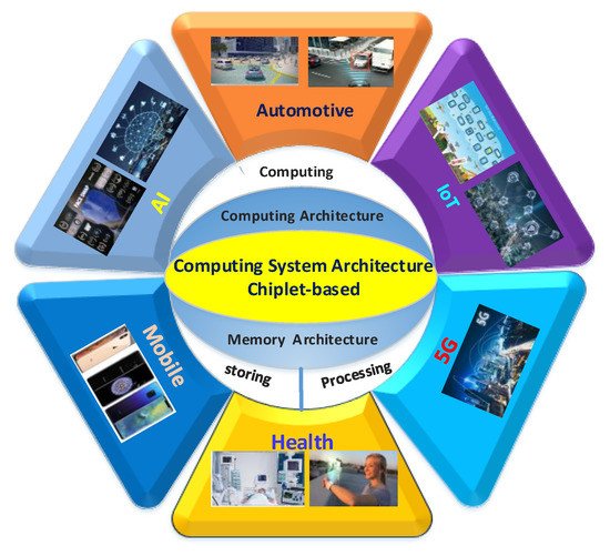
Figure 1. Computing system architectures and application.
2. Computing Architecture Based on Chiplet
As shown in Figure 2a, heterogeneous multi-core architecture has a higher efficiency than single-core and homogenous multi-core architectures [15]. In order to further improve multi-core architectures performance, more transistors were integrated into a limited area of a die; however, the leakage power of the transistor increases as the technology scaling, which severely reduces the energy efficiency of the multi-core architectures. Moreover, in order to ensure the thermal reliability of the computing system, some hardware resources in a die cannot be utilized; that is, the dark silicon effect is more obvious. The architecture of the computing system prepares the computing unit and the memory on one substrate with the same advanced technology, which is a monolithic System on Chip (SoC) and can improve its performance; however, the integration of computing, memory, control, and other IPs into the chip significantly increase the complexity of design and verification. Further, the analog and digital circuits are fabricated using different processes, so multi-manufacturing equipment has to be used in the same process, which dramatically increases the costs. In order to further improve the SoC performance, many chips are designed as dedicated chips, so the chip scalability deteriorates. For example, the performance of Apple mobile SoC processors was significantly improved through technology scaling and architecture updates while the costs obviously raised, as shown in Figure 2b [16].
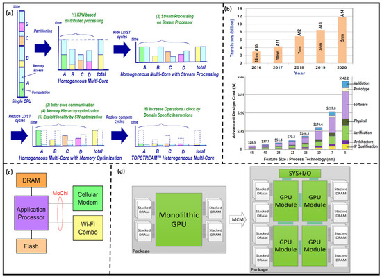
Figure 2. (a) Performance comparison of homogeneous and heterogeneous multi-core architectures. (Reprinted from [15], Copyright 2012, with permission from IEEE); (b) iPhone processor development and cost analysis. (Reprinted from [16], Copyright 2021, with permission from Springer); (c) Mochi Processor architecture. (Reprinted from [17], Copyright 2019, with permission from IEEE); (d) GPU design technology based on Chiplet. (Reprinted from [16], Copyright 2021, with permission from Linley Group, Inc.)
The computing system architecture designed by modularization and generalization Chiplet can achieve higher performance, lower complexity and cost, and it can reduce the parasitic effect by using 2.5D or 3D integration technology. The computing system architectures based on Chiplet are a key research aspect of computing architecture.
2.1. Computing Architecture Integrated with 2.5D Technology
Nurvitadhi et al. [17] compared the performance of GPU (NVIDIA Volta, 10 nm) and Chiplet-based Field Programmable Gate Array (FPGA) integrated with 2.5D integrated technology (Intel Stratix 10, 14 nm) in a given computing task (FP32, INT8). The results show that the computing powers of GPU and Chiplet-based FPGA are 6% and 57% of their peak, respectively. The delay and energy efficiency of FPGA are 1/16 and 34× of GPU, respectively. It shows that the computing system architecture based on Chiplet has higher performance and hardware utilization, as well as lower cost. Sehat [18] proposed the mobile architecture called MoChi, which is integrated by computing Chiplet (such as CPU) with advanced technology and other Chiplets with mature technology. The system resource sharing and communication can be achieved by the MoChi interface, as shown in Figure 2c. The architecture has lower design complexity compared with traditional monolithic SoC architectures. The core of the computing architecture is the integration of Chiplet from different vendors through the interface, and the advanced 2.5D integration technology can be used to reduce the number of pins and packaging costs.
Arunkumar et al. [19] decomposed a single-chip multi-core GPU into multiple GPU Chiplets to design a high-performance computing architecture, as shown in Figure 2d, which can improve computing speed by 22.8% with an energy efficiency of 0.5 pj/bit. The utilization ratio of hardware resources is increased for the GPU and DRAM Chiplet, so the dark silicon effect is alleviated. Further, the yield of the wafer is improved for the larger GPU is decomposed into multiple GPU Chiplet with a smaller area.
Based on the requirements of the National Aeronautics and Space Administration (NASA) in reconfigurable computing architecture, Mounce et al. [20] proposed a high-performance spatial heterogeneous computing architecture for space applications, as shown in Figure 3b. High-speed communication between Chiplets is implemented by standard communication protocol and bus. In addition, they proposed that the Chiplet-based approach can build more powerful heterogeneous systems with radio frequency (RF) Chiplet and FPGA, and further achieve a smaller size and lower cost. This indicates that the computing system architecture based on Chiplet can take advantage of different hardware resources and achieve higher system scalability. The system performance can be further improved through advanced packaging. Vijayaraghavan et al. [21] designed a Chiplet-based computing system for climate prediction, as shown in Figure 3a. It integrates high-throughput and energy-efficient GPU Chiplet, high-performance multi-core CPU Chiplet, and large capacity 3D memory. The system can achieve a bandwidth of 3 TB/s and power consumption of 160 W at 1 GHz. Lin et al. [22] designed a Chiplet-based high-performance computing architecture, which integrates four 7 nm ARM Cortex-A72 cores in two computing Chiplets. The Chiplet communication can be achieved through the parallel channels formed by Low-voltage-InPackage-INterCONnect technology. The bandwidth rate and density are 320 GB/s and 1.6 Tb/s/mm2 under 4 GHz, respectively. The lower roughness and smaller line spacing for the Chiplet connection can be achieved by InFO_SoW technology. The bandwidth density and power distribution network (PDN) impedance are 2× and 30% more than flip-chip multi-chip-module (MCM) interconnection, and interconnection power consumption is reduced by 15% [23], as shown in Figure 3c. In Agilex series FPGAs, the core Chiplet and other Chiplets were interconnected using Embedded Multidie Interconnect Bridge (EMIB). Compared to Stratix10, the delay is reduced by 2.5×, and the bandwidth density and energy efficiency are improved 5.68× and 2.84×, respectively [24]. The interconnect technology has no limitation on the Chiplet area compared to industrial standard 2.5D multi-chip interconnection, which permits flexible placement. The technology can improve the signal and power integrities by isolating signal and power paths, and reducing the cost due to without addition through silicon via (TSV) [25], as shown in Figure 3d. The power consumption of data transfer takes up a large proportion of the total computing system energy. One promising way to improve energy efficiency and bandwidth is to optimize the Chiplet interconnection. The commonality between InFO_SoW and EMIB lies in the preparation of high-density TSV and re-distribution layer (RDL), within the interposer. The Chiplets, interposer, substrate, and printed circuit board (PCB) were integrated by 2.5D technology, so the bandwidth, energy efficiency, signal, and power integrities were improved effectivity.
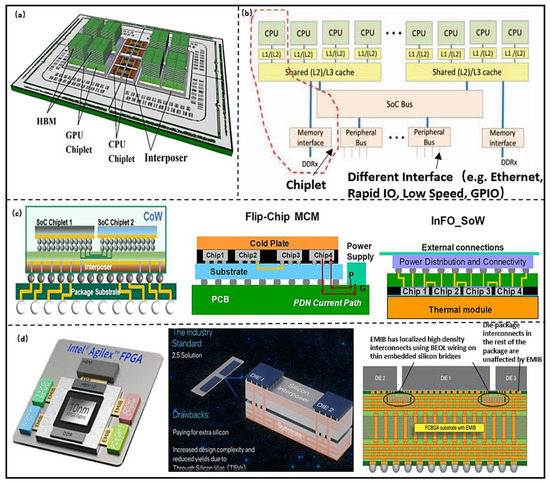
Figure 3. (a) Computing system architecture model based on Chiplet. (Reprinted from [19], Copyright 2017, with permission from IEEE); (b) Chiplet planning technology. (Reprinted from [20], Copyright 2016, with permission from IEEE) [20]; (c) TSMC high performance computing architecture based on Chiplet. (Reprinted from [21], Copyright 2017, with permission from IEEE); (d) Chiplet-based integration architecture. (Reprinted from [22], Copyright 2020, with permission from IEEE).
Zaruba et al. [26] used four computing Chiplets and high bandwidth memory (HBM) Chiplet (8 GB L1 Cache and 27 MB shared L2 memory) to construct computing architecture for high-precision floating-point computing. The computing architecture can be switched between high-performance and high-efficiency modes by reconfiguration. The peak efficiency is larger than 4 TDPflop/s, and power consumption is 25% lower than NVIDIA Volta (7 nm). The efficiency of the architecture is two times and three times that of Intel i9-9900K (14 nm) and ARM N1 (7 nm), respectively. The results show that computing architectures based on Chiplet are more easily integrated with large memory and have a high configurability. Due to the higher modularity of Chiplet, the computing system architecture can be configured in various modes according to the applications. The computing architecture has higher reconfigurability and scalability compared with the traditional SoC-based computing system. It requires co-design of software and hardware, and there is a certain design complexity. Fortunately, there are already solutions for these problems; therefore, the Chiplet-based reconfigurable computing system design technology has obvious technical advantages.
2.2. Computing Architecture Integrated with 3D Technology
Since technology scaling cannot improve the performance of digital Chiplet (CPU compute die) and analog Chiplet (IO Chiplet and memory Chiplet) in the same proportion without increasing the cost. The design method of computing architecture based on Chiplet achieves the optimization of performance and cost by selecting the combination of Chiplet with the best technology. Further, it is necessary to reduce the size of electronics driven by small form factors and the lightweight of wearable (motion watch, bodily function devices, etc.), portable electronics (mobile, laptop, etc.); therefore, more and more computing systems are designed with 3D architectures. The computing system performance can be improved by co-design of 3D architectures and advanced packing technology.
This approach is widely used by AMD in high-performance computing (HPC) system design, enabling rapid development of two products through a different number of Chiplets combinations, such as Rome and Matisse [9], as shown in Figure 4a. The most obvious advantages are that the design of the computing system is simplified and the time to market of product is reduced. The other merits of the architecture include the fact that the digital Chiplet is backward compatible with complex interfaces and the memory Chiplet; that is, the optimal combination of computing and memory Chiplets can be selected according to the computing ability requirements, which has higher scalability and reconfigurability compared with the traditional multi-core architecture and SoC computing system architectures. In order to improve energy efficiency, Kadomoto et al. [27] proposed a method to realize Chiplet communication using the mutual coupling effect of on-chip inductor coils, and fabricated a communication network using 0.18 µm process. The maximum bandwidth can reach 1.6 Gb/s, and the time variation is 3%. The total power consumption is 14.5 mW. The computing architecture has potential in medical microrobots. Although the inter-chip communication based on mutual inductance simplifies the routing design; however, electromagnetic coupling in a small volume leads to signal timing deterioration; therefore, this method requires a sufficient shielding design, which can increase the design difficulty. Burd et al. [28] proposed the infinity fabric (IF) technology to connect Chiplets for higher scalability and configurability in a computing system. It combines scalable data fabric (SDF) and scalable control fabric (SCF) as a critical enabler and utilizes 3D package routing layers to support more complex connections. The in-package bandwidth can achieve 256 GB/s with 534 IFs, and its energy efficiency is 1.2 pj/bit (2 pj/bit for EMIB). CEA-LETI [29] developed a 96-core processor by stacking 28 nm computing Chiplet on the 65 nm interposer with a power management module. The Chiplet interconnected with µbump (20 µm pitch), TSV (depth to width ratio of 10:1 and 40 µm pitch) and RDL (10 µm width and pitch of 20 µm). The Chiplets communication can be achieved by extendable Network on Chip (NoC), and the bandwidth is above 3 Tbit/s/mm2, delay below 0.6 ns/mm [30], as shown in Figure 4b. The Lakefield mobile processor also adopted multiple Chiplets design technology, which consists of the computing and memory Chiplets prepared with optimal technology (10 nm and 22 FFL). All Chiplets were bonded face to face with micro-bumps in 50 µm pitch (Foveros technology) [31]. The parasitic capacitance and resistance are below 250 fF and 70 mΩ, respectively. The data transfer rate bandwidth is up to 500 Mb/s with an energy efficiency of 0.2 pj/b. Foveros technology has good compatibility with EMIB and can be used for high-density interconnection of the same system for more flexible interconnection [32]. IF, NoC, and Foveros are all based on 3D electrical interconnection, and the preparation technology is relatively mature. The performance of the computing system is highly predictable. The computing system can obtain a high bandwidth and energy efficiency at a certain working frequency (The typical value is 1.15 GHz, as shown in Table 1); however, with the increase in operating frequency, the parasitic resistor, capacitor, and inductor of TSV and RDL can degrade the signal integrity. In addition, Joule heat produced by TSV and RDL can reduce the system reliability; therefore, more optimized interconnect technologies are needed.
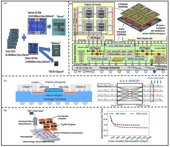
Figure 4. (a) AMD processors design technology based on Chiplet. (Reprinted from [9], Copyright 2020, with permission from IEEE); (b) INTACT computing architecture based on Chiplet. (Reprinted from [29], Copyright 2019, with permission from IEEE); (c) Hybrid optical–electrical interconnection. (Reprinted from [31], Copyright 2020, with permission from IEEE); (d) POPSTAR interconnection architecture. (Reprinted from [19], Copyright 2019, with permission from IEEE).
Table 1. Comparison of computing architectures based on Chiplet.
| Intel [24] |
TSMC [22] |
AMD [9] |
CEA-Leti [30] |
Intel [25] |
Bologna [26] |
|
|---|---|---|---|---|---|---|
| Product Name | Agilex | - | Ryzen | INTACT | Lakefield | Manticore |
| Launched Time | 201904 | 201908 | 201908 | 202002 | 202006 | 202012 |
| Chiplet Technology (nm) | 10 | 7 | 7 + 12 | FDSOI 28 | 10 + 22 FFL | GF 22 FDX |
| Chiplet Number | scalable | 2 | >2 | 6 | 1 | 4 |
| Number of cores/Chiplet | Cortex-A53 | 4 Cortex-A72 | 64 (Server) 16 (Cilient) |
16 | 1 Core+ 4 Atom |
1024 RISC-V |
| Area (mm2) | - | 4.4 × 6.2 | - | 4 × 5.6 | - | 9 |
| Bandwidth (Max) | 32 Gb/s | 320 GB/s | ~55 GB/s | 527 GB/s | ~34 GB/s | 1 TB/s |
| Bandwidth density | 1.6 Tb/s/mm2 | - | 3 Tbit/s/mm2 | - | - | |
| Frequency (GHz) | 1.5 | 4 | ~1 | 1.15 | ~1 | 1 |
| Integrated type | 2.5D | 2.5D | 3D | 3D | 3D | 2.5D |
| Interposer type | Passive | Passive | N/A | Active | Active | Yes |
| Interconnect pitch (µm) | 55 | 40 | - | 20 | 50 | 20 |
| Delay | ~60 ps | - | <9 ns | 0.6 ns/mm | - | - |
| Integration technology | EMIB | CoWoS | F2F | Foveros | - | |
| Yield | High | High | High | High | High | High |
| Scalability | High | High | High | - | ||
| Configurability | Good | Yes | Yes | Yes | alternative | High efficiency/performance |
| Reusability | High | High | High | High | High | High |
| Testability | Good | Good | Good | |||
| Power efficiency | - | 0.56 pJ/b | 2 pJ/b | 0.59 pj/b | 0.2 pJ/b | 50 Gdopflop/sW |
| Application | Data Center, Networking, Edge Computing | HPC | Server and Desktop Products | Cloud Computing Accelerators | Mobile, PC | Data Center, Networking, Edge Computing. |
Fotouhi et al. [33] proposed a 3D integration architecture that uses the hybrid Chiplet interconnect technology, as shown in Figure 4c. Silicon bridge is used for a short distance electrical interconnect transceivers (TRXs) Chiplet, and an arrayed waveguide grating router (AWGR) is used for long interconnection in wavelength division multiplexing (WDM). The computing performance is improved by 23%, while the power is reduced by 30%. Narayan et al. [34] designed an optical communication structure for data-parallel transmission between Chiplets by wavelength selection, which can save 38% energy with 1% performance degeneration, and peak bandwidth of 1750 Gb/s, as shown in Figure 4d. AWGR in [34] and interconnection technology in [35] are based on silicon photonic technology, which can realize the selective routing of optical signals by adjusting wavelengths. The higher data bandwidth, smaller signal delay, less heat, and higher energy efficiency can be achieved compared with the electrical interconnection; however, silicon photonic communication requires a high-power laser source, which is difficult to be integrated on the chip. In addition, the performance of optical devices is greatly affected by the fluctuation of the process, so the reliability is lower than the electrical interconnection. Due to the difficulty of fabrication and integration of silicon photonic devices, optical interconnection technology cannot be widely used; however, the advantages of the technology will drive the development of the integration technology, and it will be more widely used in future computing systems.
2.3. Summary
Single-core and homogeneous multi-core architectures handle task parallelization and computing acceleration under lightweight workloads. Heterogeneous computing architectures can improve energy efficiency by integrating the merits of different computing cores, such as CPU–GPU/CPU–NPU; however, multi-core architectures cannot improve computing performance and energy efficiency as further increasing intensive workloads and scaling of technology and the dark silicon effect are made worse as cores increase in number. It can achieve a single optimization for performance, energy efficiency, or scalability. In the Chiplet-based computing system, the Chiplet is prepared with the optimized technology and further integrated with 2.5/3D advanced packing technology, which has high bandwidth and energy efficiency and low data delay. As shown in Table 1, in [22], the computing architecture was constructed with the four Chiplets using 2.5D Chip on Wafer on a substrate (CoWoS) technology, and the bandwidth can be improved to 1.6 Tb/s/mm2 in high-performance computing. In [24], the delay of Agilex can be reduced to 60 ps by using 2.5D integration technology, and the architecture has high configurability and reusability. In [25], the energy efficiency of Lakefield can be improved to 0.2 pJ/b, and the architecture can be configured for PC and mobile processors. In [28], the Chiplets were prepared with the most mature technology among all computing systems; however, the delay can be reduced to 0.6 ns/mm and the bandwidth can be improved to 527 GB/s through 3D integration. In [26], the interconnect pitch between μbumps can be reduced to 20 µm through 2.5D integration, and the maximum bandwidth reaches 1 TB/s. Due to the mature preparation technology of electrical interconnection and higher energy efficiency of silicon photon interconnection, these two technologies have obvious application advantages in Chiplet-based computing system architecture.
The Chiplet-based 2.5D and 3D integrated architectures have obvious advantages; however, the diversified applications have different focuses. In terms of data bandwidth, the 3D integrated architecture is better, which requires better thermal design. This architecture is more suitable for high-performance computing, for example, data center, networking, server, etc. In terms of cost, the 2.5D integrated architecture does not require a multi-layer Interposer with high-density TSVs; thus, the process is less difficult. The architecture is more suitable for applications such as mobile, laptop, wearable electronics, etc. In terms of Chiplet materials, due to the same thermal expansion coefficient, multiple homogeneous Chiplets adopt the 3D integrated architecture, which is beneficial to improve mechanical reliability; heterogeneous Chiplets are more suitable for the 2.5D integrated architecture (such as EMIB integration technology), which has the higher performance of system heat dissipation, while its area will be increased.
References
- Mosquera-Lopez, C.; Agaian, S.; Velez-Hoyos, A.; Thompson, I. Computer-Aided Prostate Cancer Diagnosis From Digitized His topathology: A Review on Texture-Based Systems. IEEE Rev. Biomed. Eng. 2015, 8, 98–113.
- Traub, M.; Maier, A.; Barbehön, K.L. Future Automotive Architecture and the Impact of IT Trends. IEEE Softw. 2017, 34, 27–32.
- Okeme, P.A.; Skakun, A.D.; Muzalevskii, R.A. Transformation of Factory to Smart Factory; IEEE ElConRus: Moscow, Russia, 2021; pp. 1499–1503.
- Design and Visualization. Available online: https://www.nvidia.cn/design-visualization/solutions/engineering-simulation/ (accessed on 26 November 2021).
- The Tick-Tock Model Through the Years. Available online: https://www.intel.com/content/www/us/en/silicon-innovations/intel-tick-tock-model-general.html (accessed on 26 November 2021).
- Nothing Stacks up to EPYC. Available online: https://www.amd.com/zh-hans (accessed on 26 November 2021).
- Vangal, S.; Paul, S.; Hsu, S.; Agarwal, A.; Kumar, S.; Krishnamurthy, R.; Krishnamurthy, H.; Tschanz, J.; De, V.; Kim, C.H. Wide-Range Many-Core SoC Design in Scaled CMOS: Challenges and Opportunities. IEEE Trans. VLSI Syst. 2021, 29, 843–856.
- IEEE Electronics Packaging Society. Available online: https://eps.ieee.org/technology/heterogeneous-integration-roadmap/2019-edition.html (accessed on 26 November 2021).
- Naffziger, S.; Lepak, K.; Paraschou, M.; Subramony, M. 2.2 AMD Chiplet Architecture for High-Performance Server and Desktop Products. In Proceedings of the IEEE International Solid-State Circuits Conference, San Francisco, CA, USA, 16–20 February 2020; pp. 44–45.
- Moore, S.K. Chiplets are the future of processors: Three advances boost performance, cut costs, and save powe. IEEE Spectr. 2020, 55, 11–12.
- Stow, D.; Xie, Y.; Siddiqua, T.; Loh, G.H. Cost-effective design of scalable high-performance systems using active and passive interposers. In Proceedings of the IEEE/ACM International Conference on Computer-Aided Design (ICCAD), San Jose, CA, USA, 13–16 November 2017; pp. 728–735.
- Schulte, M.J.; Ignatowski, M.; Loh, G.H. Achieving Exascale Capabilities through Heterogeneous Computing. IEEE Micro 2015, 35, 26–36.
- Esmaeilzadeh, H.; Blem, E.; Amant, R.S.; Sankaralingam, K.; Burger, D. Dark Silicon and the End of Multicore Scaling. In Proceedings of the 38th International Symposium on Computer Architecture (ISCA), San Jose, CA, USA, 4–8 June 2011; IEEE: Washington, DC, USA; pp. 365–376.
- Pal, S.; Petrisko, D.; Kumar, R.; Gupta, P. Design Space Exploration for Chiplet-Assembly-Based Processors. IEEE Trans. VLSI Syst. 2020, 8, 1062–1073.
- Matsumoto, Y.; Morimoto, T.; Hagimoto, M.; Uchida, H.; Hikichi, N.; Imura, F.; Nakagawa, H.; Aoyagi, M. Cool System scalable 3-D stacked heterogeneous Multi-Core / Multi-Chip ar chitecture for ultra low-power digital TV applications. In Proceedings of the IEEE COOL Chips XV, Yokohama, Japan, 18–20 August 2012; pp. 1–3.
- Lau, J.H. Semiconductor Advanced Packaging; Springer: Berlin, Germany, 2021; pp. 414–415.
- Nurvitadhi, E.; Kwon, D.; Jafari, A.; Boutros, A.; Sim, J.; Tomson, P.; Sumbul, H.; Chen, C.; Knag, P.; Kumar, R.; et al. Why Compete When You Can Work Together: FPGA-ASIC Integration for Persistent RNNs. In Proceedings of the IEEE 27th Annual International Symposium on Field-Programmable Custom Computing Machines (FCCM), San Diego, CA, USA, 28 April–1 May 2019; pp. 199–207.
- Microprocessor Report. Available online: https://www.linleygroup.com/mpr/archive.php?j=MPR&year=2015 (accessed on 26 November 2021).
- Arunkumar, A.; Bolotin, E.; Cho, B.; Milic, U.; Ebrahimi, E.; Villa, O.; Jaleel, A.; Jean, C.J.; Nellans, D. MCM-GPU: Multi-chip-module GPUs for continued performance scalability. In Proceedings of the ACM/IEEE 44th Annual International Symposium on Computer Architecture (ISCA), Toronto, ON, Canada, 24–28 June 2017; pp. 320–332.
- Mounce, G.; Lyke, J.; Horan, S.; Powell, W.; Doyle, R.; Some, R. Chiplet based approach for heterogeneous processing and packaging architectures. In Proceedings of the IEEE Aerospace Conference, Big Sky, MT, USA, 5–12 April 2016; pp. 1–12.
- Vijayaraghavan, T.; Eckert, Y.; Loh, G.H.; Schulte, M.J.; Ignatowski, M.; Beckmann, B.M.; Brantley, W.C.; Greathouse, J.L.; Huang, W.; Karunanithi, A.; et al. Design and Analysis of an APU for Exascale Computing. In Proceedings of the IEEE International Symposium on High Performance Computer Architecture (HPCA), Austin, TX, USA, 4–8 February 2017; pp. 85–96.
- Lin, M.-S.; Huang, T.-C.; Tsai, C.-C.; Tam, K.-H.; Hsieh, K.C.-H.; Chen, C.-F.; Huang, W.-H.; Hu, C.-W.; Chen, Y.-C.; Goel, S.K.; et al. A 7-nm 4-GHz Arm¹-Core-Based CoWoS¹ Chiplet Design for High-Performance Computing. IEEE. J. Solid-State Circuits 2020, 55, 956–966.
- Chun, S.R.; Kuo, T.H.; Tsai, H.Y.; Liu, C.-S.; Wang, C.-T.; Hsieh, J.-S.; Lin, T.-S.; Ku, T.; Yu, D. InFO_SoW (System-on-Wafer) for High Performance Computing. In Proceedings of the 2020 IEEE 70th Electronic Components and Technology Conference (ECTC), Orlando, FL, USA, 3–30 June 2020; pp. 1–6.
- Ganusov, K.; Iyer, M.A.; Cheng, N.; Meisler, A. Agilex™ Generation of Intel® FPGAs. In Proceedings of the 2020 IEEE Hot Chips 32 Symposium (HCS), Palo Alto, CA, USA, 16–18 August 2020; pp. 1–26.
- Keser, B.; Kroehnert, S. Embedded Multi-die Interconnect Bridge. In Advances in Embedded and Fan-Out Wafer Level Packaging Technologies; Keser, B., Kroehnert, S., Eds.; Wiley-IEEE Press: Chandler, AZ, USA, 2019; Volume 23, pp. 487–499.
- Zaruba, F.; Schuiki, F.; Benini, L. A 4096-core RISC-V Chiplet Architecture for Ultra-efficient Floating-point Computing. In Proceedings of the IEEE Hot Chips 32 Symposium (HCS), Palo Alto, CA, USA, 16–18 August 2020; pp. 1–24.
- Kadomoto, J.; Irie, H.; Sakai, S. A RISC-V Processor with an Inter-Chiplet Wireless Communication Interface for Shape-Changeable Computers. In Proceedings of the IEEE Symposium in Low-Power and High-Speed Chips (COOL CHIPS), Kokubunji, Japan, 15–17 April 2020; pp. 1–3.
- Burd, T.; Beck, N.; White, S.; Paraschou, M.; Naffziger, S. Zeppelin: An SoC for multichip architectures. IEEE J. Solid-State Circuits 2019, 54, 40–42.
- Coudrain, P.; Charbonnier, J.; Garnier, A.; Vivet, P.; Vélard, R.; Vinci, A.; Ponthenier, F.; Farcy, A.; Segaud, R.; Chausse, P.; et al. Active Interposer Technology for Chiplet-Based Advanced 3D System Architectures. In Proceedings of the 2019 IEEE 69th Electronic Components and Technology Conference (ECTC), Las Vegas, NV, USA, 28–31 May 2019; pp. 569–578.
- Vivet, P.; Guthmuller, E.; Thonnart, Y.; Pillonnet, G.; Fuguet, C.; Miro-Panades, I.; Moritz, G.; Durupt, J.; Bernard, C.; Varreau, D.; et al. IntAct: A 96-Core Processor With Six Chiplets 3D-Stacked on an Active Interposer With Distributed Interconnects and Integrated Power Management. IEEE. J. Solid-State Circuits 2021, 56, 79–97.
- Gomes, W.; Khushu, S.; Ingerly, D.B.; Stover, P.N.; Chowdhury, N.I.; O’Mahony, F.; Balankutty, A.; Dolev, N.; Dixon, M.G.; Jiang, L.; et al. 8.1 Lakefield and Mobility Compute: A 3D Stacked 10 nm and 22FFL Hybrid Processor System in 12 × 12 mm2, 1 mm Package-On-Package. In Proceedings of the IEEE International Solid-State Circuits Conference—(ISSCC), San Francisco, CA, USA, 16–20 February 2020.
- Ingerly, D.B.; Enamul, K.; Gomes, W.; Jones, D.; Kolluru, K.C.; Kandas, A.; Kim, G.-S.; Ma, H.; Pantuso, D.; Petersburg, C.; et al. Foveros: 3D Integration and the use of Face-to-Face Chip Stacking for Logic Devices. In Proceedings of the IEEE International Electron Devices Meeting (IEDM), San Francisco, CA, USA, 7–11 December 2019; pp. 19.6.1–19.6.4.
- Fotouhi, P.; Werner, S.; Lowe-Power, J.; Yoo, S.J.B. Enabling scalable chiplet-based uniform memory architectures with silicon photonics. In Proceedings of the International Symposium on Memory Systems (MEMSYS ‘19), New York, NY, USA, 30 September–3 October 2019.
- Narayan, A.; Thonnart, Y.; Vivet, P.; Joshi, A.; Coskun, A.K. System-level Evaluation of Chip-Scale Silicon Photonic Networks for Emerging Data-Intensive Applications. 2020 Design. In Proceedings of the Automation & Test in Europe Conference & Exhibition (DATE), Grenoble, France, 9–13 March 2020.
- Ausavarungnirun, R.; Chang, K.K.; Subramanian, L.; Loh, G.H.; Mutlu, O. Staged memory scheduling: Achieving high performance and scalability in heterogeneous systems. In Proceedings of the 39th Annual International Symposium on Computer Architecture (ISCA), Portland, OR, USA, 9–13 June 2012; pp. 416–427.
More