Silicon nitride (SiNx) and hydrogenated silicon nitride (SiNx:H) thin films enjoy widespread scientific interest across multiple application fields. Exceptional combination of optical, mechanical, and thermal properties allows for their utilization in several industries, from solar and semiconductor to coated glass production. Historically different types of chemical vapour deposition (CVD), such as plasma enhanced (PE-CVD) or hot wire (HW-CVD) are the most common deposition methods, while physical vapour deposition (PVD), primarily sputtering is also widely used. Besides these fabrication methods, atomic layer deposition (ALD) is an emerging technique due to its ability to control the deposition at atomic level and provide extremely thin SiNx layers. Application of these three deposition methods is compared while special attention is paid to the effect of fabrication method on the properties of SiNx thin films, in particular the optical, mechanical, and thermal properties.
- SiNx thin films
- chemical vapor deposition
- radio frequency sputtering
- atomic layer deposition
1. Introduction
Apart from the photovoltaic devices, which have enhanced transmittance in the visible wavelength range and increased reflectance in the far infrared range, SiNx layers are a suitable material for low-emissivity (LowE) glass coatings, which are utilized in architectural glazings to mitigate heat losses in architectural applications. In this case, multilayer stacks, which usually composed of dielectric/metal/dielectric layers, are deposited on the glass surface, where the role of the silver layer is to reflect IR radiation back to the inside of the building and the dielectric materials protect the silver as well as act as antireflection layers. SiNx thin films usually deposited by magnetron sputtering are often used as dielectric layers in such applications [15][1].
Stochiometric silicon nitride (Si 3N 4) exists in three different crystallographic structures, namely α, β, and γ phases [16][2]. While the most common α and β phases can be synthesized under normal pressure, the formation of the γ phase requires high pressure and temperature conditions [17][3]. Amorphous silicon nitride (a-SiNx) presents a wide range of layer properties that are a function of the structure and bonding configuration as well as of the composition of the film. Tailoring the refractive index of a-SiNx is feasible by controlling the N/Si ratio of the films [18,19,20][4][5][6].
Fabrication technologies of SiNx layers are generally divided into two main techniques, namely the chemical vapor deposition (CVD) technique and the physical vapor deposition (PVD) technique, which are based on the types of involved reactions during deposition. In the case of CVD methods, the material introduced to the deposition chamber in the gas phase is deposited as a result of chemical reactions on the substrate surface where a thin film is grown. Additionally, a common feature of PVD methods is that the material, which is initially typically in the solid phase, is transformed to the gas phase, after which the material then returns to a solid phase by creating a layer on the desired substrate. In the case of PVD techniques, sputtering is the method predominantly used, while for CVD technologies, several different processes, e.g., hot wire (HW-CVD) [21[7][8],22], expanded thermal plasma (ETP-CVD) [23][9], electron cyclotron resonance (ECR-CVD) [24,25,26[10][11][12][13],27], and both plasma enhanced (PE-CVD) [28,29,30][14][15][16] and remote plasma enhanced (RPE-CVD) [31][17], are applied for the deposition of silicon nitride thin films. Due to the demand for extraordinary thin SiNx layers with precisely controlled composition and layer properties, increasing scientific interest appeared for a subset of CVD, namely the atomic layer chemical vapor deposition (ALCVD) or atomic layer deposition (ALD). In these processes, the thin film is formed on the substrate by atomic layers using chemical reactions in the gas atmosphere. For the deposition of SiNx thin films that are thermal [32,33[18][19][20],34], plasma-assisted (PA), and plasma-enhanced (PE) [35,36[21][22][23][24],37,38], ALD are the method most often used. Considering the growing scientific interest ALD methods are receiving in recent years, we discuss them separately from other CVD methods.
2. Physical Vapor Deposition
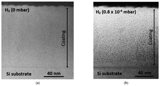
In the case of SiNx deposition, sputtering is the most common technique in which the solid state material (which is called the target in this process) is brought to the vapor phase by means of bombarding the material with electrically charged particles, causing atoms and groups of atoms to escape from its surface. The advantage of sputtering in the SiNx deposition process is the ability to fabricate hydrogen-free layers due to the lack of hydrogen-containing precursor gases. Additionally, this technique also allows for the fabrication of hydrogenated silicon nitride (SiNx:H) films by introducing hydrogen as an additional process gas. It was proven in one of our previous works [74][25] that the hydrogen incorporation into RF sputtered SiNx layers has a significant effect on the layer porosity. As shown in Figure 31, high-angle annular dark field scanning transmission electron microscopy (HAADF STEM) confirmed denser SiNx films for hydrogen-free sputtering than for the hydrogenated sputtering process, which resulted in a porous structure of the thin films with homogenously distributed nanometer-scale porosities.
In magneto-optical (MO) recording applications, amorphous SiNx layers are used as protecting dielectric films for amorphous rare earth-transition metal (RE-TM) coatings, which are the functional layers of the MO medium. In such an application, the process wherein the device writes is a thermal writing process in which thermal cycles are appended to MO disks. As a result of the thermal expansion coefficient difference between the layers and substrates, thermal stress could appear within the thermal cycle. Lai et al. [85][26] characterized the thermal stress of SiNx films at temperatures varying between 25 and 400 °C. During the heating processes, the stress was almost constant, while after the second thermal cycle, the residual stress switched from compressive (~−780 MPa) to tensile (~1050 MPa).
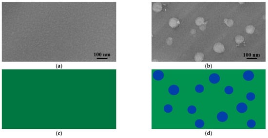
During heat treatment, a part of the silicon–hydrogen (Si–H) and nitrogen–hydrogen (N–H) bonds of the SiNx:H thin films broke. Consequently, molecular hydrogen was formed, which was then released either to the environment or towards the substrate, playing an important role in the densification of the layer as well as in the formation of its passivation behavior [31][17]. A similar surface deformation (surface blistering) was found by Jafari et al. [73][27] for PE-CVD SiNx: H thin films (presented in Section 2.5 ), wherein RF sputtered SiNx: H thin films at an even lower temperature (~65 °C). Figure 42 presents the scanning electron microscope (SEM) images of the a-SiNx:H layer surfaces prior to and after the heat treatment.
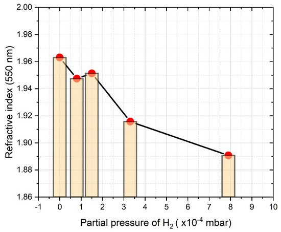
In the case of the deposition of SiNx:H thin films by the introduction of molecular hydrogen to the chamber, control of the hydrogen pressure serves as an alternative technique for tuning the refractive index of the thin films. Mokkedem et al. [90][28] studied the correlation of the hydrogen gas pressure and the refractive index of DC magnetron sputtered SiNx:H layers. It was revealed that when the partial pressure of H 2 increased from 4.5 to 9 mPa, the refractive index showed a decreasing trend from 1.92 to 1.78. Considering that, in parallel, the increase of the nitrogen to silicon ([N]/[Si]) ratio from 1.03 to 1.22, as well as the increase of the hydrogen to silicon ([H]/[Si]) ratio from 1.47 to 1.65 were proved, the experienced variations of the refractive index should be attributed to the incorporation of H and N atoms into the layers. We experienced a similar correlation between the partial pressure of the hydrogen applied to the chamber and the refractive index at 550 nm of SiNx:H layers prepared by RF sputtering, as shown in Figure 53 [74][25].
3. ALD
The atomic layer deposition (ALD) is a subclass of CVD based on sequential gas-phase chemical processes. Since this method allows for low temperature deposition as well as for the control of the film thickness with precision in the atomic scale, it has attracted great scientific interest concerning SiNx layer fabrication in recent years. In this section, current research progress, the most important trends, and future prospects are summarized.
Thermal ALD relies on the heating of the deposition chamber and the substrate to drive the surface reaction kinetics; therefore, higher deposition temperature (typically above 450 °C) is required. In the majority of the related works, chlorosilanes as silicon-containing precursors and ammonia as a nitrogen source are applied [94,95,96,97,98,99][29][30][31][32][33][34]. Additionally, Morishita et al. [100][35] revealed that SiNx can be also deposited by thermal ALD from Si 2Cl 6 between temperatures of 525 and 650 °C. It should be also noted that we are not aware of any thermal ALD SiNx which was produced from non-chlorosilane-based precursors. Riedel et al. [98][33] investigated thermal ALD SiNx layers deposited at various substrate temperatures varying from 310 to 500 °C, utilizing octachlorotrisilane (OCTS, Si 3Cl 8) as an alternative Si-containing precursor gas and NH 3 as a N source. They found that the wet etch rates in diluted HF (100:1–0.49%) decreased versus the raising substrate temperature and thus increasing film density. Significant amounts of oxygen were also found, the quantity of which shows a decreasing trend with an increasing deposition temperature. In the absence of an oxygen source, we can assume that the layers were oxidizing because of the contact with the ambient air. Park et al. [97][32] also found that thermal ALD SiNx layers are non-stochiometric and can be simply oxidized by air exposures, leading to approximately 7–8 atomic % O content of the thin film.
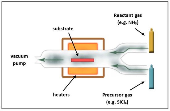
In order to overwhelm the difficulties of the increased deposition temperature of thermal ALD methods and to meet the requirements of modern (e.g., interconnect and spacer) applications [93[36][35][37],100,101], plasma-enhanced ALD is utilized in several cases. This technique was proved to be an appropriate method to deposit silicon nitride at T < 400 °C by several researchers [102,103,104,105][38][39][40][41]. Furthermore, the enhanced reactivity of the plasma allows for the application of precursors which don’t contain halogen atoms [106,107,108,109][42][43][44][45]. Deposition temperature can be further decreased by remotely generated plasma, which is then transported to the chamber [110,111,112,113,114,115][46][47][48][49][50][51]. In Figure 64 , a schematic drawing of a PE-ALD reactor is presented.
In addition to the lower deposition temperature, this method is also advantageous in minimizing plasma-induced damages and surface nucleation time, as well as in avoiding undesirable gas-phase reactions. Several reports studied how the substrate temperature influences the PE ALD process. Andringa et al. [116][52] characterized the refractive index and the chemical composition of SiNx moisture permeation barrier layers fabricated by PE ALD with the SiH 2(NH t BU) 2 precursor and by nitrogen-fed plasma at different deposition temperatures. It was revealed that the refractive index (at 633 nm) was increased from 1.8 to 1.9, while the deposition temperature was raised from 80 to 200 °C. In contrast, carbon, oxygen, and hydrogen impurity levels showed decreasing trends against increasing deposition temperatures. In terms of porosity, they found that there were no open pores with diameters bigger than 0.3 nm independently from the deposition temperature. Jang et al. [108][44] studied the effect of temperature on SiNx deposition by PE-ALD from trisilylamine [TSA, (SiH 3) 3N] and NH 3 in the range of 250–350 °C. However, it was revealed that all films are near-stochiometric and the N/Si stochiometric ratio slightly increases (from 1.32 to 1.35) due to the increase of the deposition temperature (from 250 to 350 °C). Higher temperatures resulted in higher refractive indices as well as lower hydrogen contents. The effect of the temperature on the defect density was also proved since increased deposition temperatures led to enhanced trap densities, which should be attributed to the lower hydrogen content. The latter behavior allows for adjusting the defect densities to meet the requirements of charge trap flash memory applications by controlling the fabrication temperature. Another work [117][53] introduces low-temperature (250–300 °C) PE-ALD of SiNx, utilizing neopentasilane [NPS, (SiH 3) 4Si] with a direct N 2 plasma. The thin film deposition was compared to a more frequently used source gas, specifically trisilylamine [TSA, (SiH 3) 3N], as a reference. In terms of the growth behavior and N 2 plasma saturation, no significant differences were found. However, higher growth rates were observed for NPS. It was revealed that increased N 2 plasma exposure time caused a decrease in the refractive index for both precursors. Koehler et al. [118][54] investigated SiNx thin films deposited at higher temperatures (400–500 °C) by ALD for spacer and gate encapsulation applications. They found that the SiNx film quality and growth conditions have important roles in shaping the performance of high-k metal gate technology.
4. Conclusions
A combination of advantageous layer properties establishes SiNx thin films a promising candidate for several application fields. In this work, an overview of the latest published works for SiNx thin films was presented with a focus on the applications and obtainable layer properties by applying different deposition methods. The latest achievements of CVD and PVD depositions technologies were highlighted with a comparison of their characteristic mechanical, thermal, and optical properties. In view of the growing demand for ultrathin SiNx layers with precise control of the composition, a group of CVD methods (ALCVD) was reviewed in a separate section.
In terms of deposition temperature, a trend towards lower processing temperatures was observed due to efforts to minimize the damage of thermally instable substrates, such as IC applications or polymer materials of OLED devices. Another trend of the development of SiNx thin films concerned targeting to achieve better mechanical properties, driven by hard coating applications under challenging environmental conditions.
Obviously, SiNx layer properties are affected by several parameters such as the fabrication method, precursor gas chemistry, type of power supply used for the plasma generation, and the substrate temperature. However, the exact correlation between the process parameters and the layer properties could depend on the actual deposition equipment. The results reviewed in this paper could act as a guideline for the development and further tuning of SiNx layer properties to meet the expectations of certain applications.
References
- Kulczyk-Malecka, J.; Kelly, P.; West, G.; Clarke, G.C.B.; Ridealgh, J. Diffusion studies in magnetron sputter deposited silicon nitride films. Surf. Coatings Technol. 2013, 255, 37–42.
- Dressler, W.; Riedel, R. Progress in silicon based non-oxide structural ceramics. Int. J. Refract. Metals Hard Mater. 1997, 15, 13–47.
- Jiang, J.Z.; Kragh, F.; Frost, D.; Lindelov, H. Hardness and thermal stability of cubic silicon nitride. J. Physics Condens. Matter 2001, 13, L515–L520.
- Ku, S.-L.; Lee, C.-C. Optical and structural properties of silicon nitride thin films prepared by ion-assisted deposition. Opt. Mater. 2010, 32, 956–960.
- Budaguan, B.G.; Stryahilev, D.A.; Aivazov, A.A. Optical properties, statistics of bond angle deformations and density of states in Si-rich a-SiNx: H alloys. J. Non-Cryst. Solids 1997, 210, 267–274.
- Vargheese, K.D.; Rao, G.M. Electrical properties of silicon nitride films prepared by electron cyclotron resonance assisted sputter deposition. J. Vac. Sci. Technol. A 2001, 19, 2122–2126.
- Verlaan, V.; van der Werf, C.H.M.; Houweling, Z.S.; Romijn, I.G.; Weeber, A.W.; Dekkers, H.F.W.; Goldbach, H.D.; Schropp, R.E.I. Multi-crystalline Si solar cells with very fast deposited (180 nm/min) passivating hot-wire CVD silicon nitride as antireflection coating. Prog. Photovoltaics Res. Appl. 2007, 15, 563–573.
- Deshpande, S.V.; Gulari, E.; Brown, S.W.; Rand, S.C. Optical properties of silicon nitride films deposited by hot filament chemical vapor deposition. J. Appl. Phys. 1995, 77, 6534–6541.
- Kessels, W.M.M.; Hong, J.; van Assche, F.J.H.; MOschner, J.D.; Lauinger, T.; Soppe, W.J.; Weeber, A.W.; Schram, D.C.; van de Sanden, M.C.M. High-rate deposition of a-SiNx:H for photovoltaic application y the expanding thermal plasma. J. Vac. Sci. Technol. A 2002, 20, 1704.
- Martınez, F.L.; Ruiz-Merino, R.; Del Prado, A.; San Andrés, E.; Mártil, I.; González-Dıaz, G.; Jeynes, C.; Barradas, N.P.; Wang, L.; Reehal, H.S. Bonding structure and hydrogen content in silicon nitride thin films deposited by electron cyclotron resonance plasma method. Thin Solid Films 2004, 459, 203–207.
- San Andrés, E.; Del Prado, A.; Martınez, F.L.; Mártil, I.; Bravo, D.; López, F.J. Rapid thermal annealing effects on the structural properties and density of defects in SiO2 and SiNx:H films deposited by electron cyclotron resonance. J. Appl. Phys. 2000, 87, 1187–1192.
- Martil, I.; del Prado, A.; San Andres, E.; Gonzalez Daz, G.; Martnez, F.L. Rapid thermally annealed plasma deposited SiNx:H thin films: Application to metal-insulator-semiconductor structures with Si, In0.53 Ga0.47 As, and InP. J. Appl. Phys. 2003, 94, 2642.
- Martnez, F.L.; del Prado, A.; Martil, I.; Gonzalez-Daz, G.; Selle, B.; Sieber, I. Thermally induced changes in the optical properties of SiNx:H films deposited by the electron cyclotron resonance plasma method. J. Appl. Phys. 1999, 86, 2055.
- Bommali, R.K.; Ghosh, S.; Khan, S.A.; Srivastava, P. Hydrogen loss and its improved retention in hydrogen plasma treated a-SiNx:H films:ERDA study with 100 MeV ag7+ ions. Nucl. Instrum. Methods Phys. Res. B 2018, 423, 16–21.
- Yoo, J.; So, J.; Yu, G.; Yi, J. Study on hydrogenated silicon nitride for application of high efficiency crystalline silicon solar cells. Sol. Energy Mater. Sol. Cells 2011, 95, 7–10.
- Fitzner, M.; Abelson, J.; Kanicki, J. Investigation of Hydrogen and Nitrogen Thermal Stability in PECVD a-Sinx:H. MRS Online Proc. Libr. Arch. 2011, 258.
- Santos-Filho, P.; Stevens, G.; Lu, Z.; Koh, K.; Lucovsky, G. Hydrogen Release and Si-N Bond-Healing Infrared Study of Rapid Thermal Annealed Amorphous Silicon Nitride Thin Films. MRS Online Proc. Libr. 1995, 398.
- Edmonds, M.; Sardashti, K.; Wolf, S.; Chagarov, E.; Clemons, M.; Kent, T.; Park, J.H.; Tang, K.; McIntyre, P.C.; Yoshida, N.; et al. Low temperature thermal ALD of a SiNx interfacial diffusion barrier and interface passivation layer on SixGe1−x(001) and SixGe1− x(110). J. Chem. Phys. 2017, 146, 052820.
- Nakajima, A.; Khosru, Q.D.M.; Yoshimoto, T.; Yokoyama, S. Atomic-layer-deposited silicon-nitride/SiO2 stack—A highly potential gate dielectrics for advanced CMOS technology. Microelectron. Reliab. 2002, 42, 1823–1835.
- Zhu, S.; Nakajima, A. Atomic Layer Deposition of HfO2and Si Nitride on Ge Substrates. Jpn. J. Appl. Phys. 2007, 46, 7699–7701.
- Cho, H.; Lee, N.; Choi, H.; Park, H.; Jung, C.; Song, S.; Yuk, H.; Kim, Y.; Kim, J.-W.; Kim, K.; et al. Remote Plasma Atomic Layer Deposition of SiNx Using Cyclosilazane and H2/N2 Plasma. Appl. Sci. 2019, 9, 3531.
- Murray, C.A.; Elliott, S.D.; Hausmann, D.; Henri, J.; Lavoie, A. Effect of Reaction Mechanism on Precursor Exposure Time in Atomic Layer Deposition of Silicon Oxide and Silicon Nitride. ACS Appl. Mater. Interfaces 2014, 6, 10534–10541.
- Eom, T.-K.; Kim, S.-H.; Kang, D.-H.; Kim, H. Characteristics of Plasma-Enhanced Atomic Layer Deposited RuSiN as a Diffusion Barrier against Cu. J. Electrochem. Soc. 2011, 158, D657.
- Eom, T.K.; Kim, S.H.; Park, K.S.; Kim, S.; Kim, H. Formation of Nano-Crystalline Ru-Based Ternary Thin Films by Plasma-Enhanced Atomic Layer Deposition. Electrochem. Solid-State Lett. 2011, 14, D10–D12.
- Hegedüs, N.; Lovics, R.; Serényi, M.; Zolnai, Z.; Petrik, P.; Mihály, J.; Fogarassy, Z.; Balázsi, C.; Balázsi, K. Examination of the Hydrogen Incorporation into Radio Frequency-Sputtered Hydrogenated SiNx Thin Films. Coatings 2021, 11, 54.
- Lai, C.H.; Huang, C.L.; Hsu, C.Y.; Lin, I.N.; Jou, J. Optical and thermal properties of SiNx for MO disks. In Proceedings of SPIE—The International Society for Optical Engineering; International Society for Optics and Photonics, SPIE: Bellingham, WA, USA, 2012.
- Jafari, S.; Hirsch, J.; Lausch, D.; John, M.; Bernhard, N.; Meyer, S. Composition limited hydrogen effusion rate of a-SiNx:H passivation stack. AIP Conf. Proc. 2019, 2147, 050004.
- Mokeddem, K.; Aoucher, M.; Smail, T. Hydrogenated amorphous silicon nitride deposited by DC magnetron sputtering. Superlattices Microstruct. 2006, 40, 598–602.
- Yokoyama, S.; Ikeda, N.; Kajikawa, K.; Nakashima, Y. Atomic-layer selective deposition of silicon nitride on hydro-gen-terminated Si surfaces. Appl. Surf. Sci. 1998, 130–132, 352–356.
- Hansch, W.; Nakajima, A.; Yokoyama, S. Characterization of silicon/oxide/nitride layers by x-ray photoelectron spec-troscopy. Appl. Phys. Lett. 1999, 75, 1535–1537.
- Nakajima, A.; Khosru, Q.D.M.; Yoshimoto, T.; Kidera, T.; Yokoyama, S. Low-temperature formation of highly reliable silicon-nitride gate dielectrics with suppressed soft-breakdown phenomena for advanced complementary met-al-oxide-semiconductor technology. J. Vac. Sci. Technol. 2002, 20, 1406–1409.
- Park, K.; Yun, W.D.; Choi, B.J.; Kim, H.D.; Lee, W.J.; Rha, S.K.; Park, C.O. Growth studies and characterization of sili-con nitride thin films deposited by alternating exposures to Si2Cl6 and NH3. Thin Solid Films 2009, 517, 3975–3978.
- Riedel, S.; Sundqvist, J.; Gumprecht, T. Low temperature deposition of silicon nitride using Si3Cl8. Thin Solid Films 2015, 577, 114–118.
- Yusup, L.L.; Park, J.-M.; Noh, Y.-H.; Kim, S.-J.; Lee, W.-J.; Park, S.; Kwon, Y.-K. Reactivity of different surface sites with silicon chlorides during atomic layer deposition of silicon nitride. RSC Adv. 2016, 6, 68515–68524.
- Morishita, S.; Sugahara, S.; Matsumura, M. Atomic-layer chemical-vapor-deposition of silicon-nitride. Appl. Surf. Sci. 1997, 112, 198–204.
- Klaus, J.; Ott, A.; Dillon, A.; George, S. Atomic layer controlled growth of Si3N4 films using sequential surface reactions. Surf. Sci. 1998, 418, L14–L19.
- Nakajima, A.; Khosru, Q.D.M.; Yoshimoto, T.; Kidera, T.; Yokoyama, S. NH3-annealed atomic-layer-deposited silicon nitride as a high-k gate dielectric with high reliability. Appl. Phys. Lett. 2002, 80, 1252–1254.
- Goto, H.; Shibahara, K.; Yokoyama, S. Atomic layer controlled deposition of silicon nitride with self-limiting mechanism. Appl. Phys. Lett. 1996, 68, 3257–3259.
- Yokoyama, S.; Goto, H.; Miyamoto, T.; Ikeda, N.; Shibahara, K. Atomic layer controlled deposition of silicon nitride and in situ growth observation by infrared reflection absorption spectroscopy. Appl. Surf. Sci. 1997, 112, 75–81.
- Knoops, H.C.; Braeken, E.M.; de Peuter, K.; Potts, S.E.; Haukka, S.; Pore, V.; Kessels, W.M. Atomic Layer Deposi-tion of Silicon Nitride from Bis(tertbutylamino)silane and N2 plasma. Appl. Mater. Interfaces 2015, 7, 19857–19862.
- Ovanesyan, R.A.; Hausmann, D.M.; Agarwal, S. Low-Temperature Conformal Atomic Layer Deposition of SiNx Films Using Si2Cl6 and NH3 Plasma. ACS Appl. Mater. Interfaces 2015, 7, 10806–10813.
- King, S.W. Plasma enhanced atomic layer deposition of SiNx:H and SiO2. J. Vac. Sci. Technol. A 2011, 29, 041501.
- Triyoso, D.H.; Hempel, K.; Ohsiek, S.; Jaschke, V.; Shu, J.; Mutas, S.; Dittmar, K.; Schaeffer, J.; Utess, D.; Lenski, M. Evaluation of Low Temperature Silicon Nitride Spacer for High-k Metal Gate Integration. ECS J. Solid State Sci. Technol. 2013, 2, N222.
- Jang, W.; Jeon, H.; Kang, C.; Song, H.; Park, J.; Kim, H.; Seo, H.; Leskela, M.; Jeon, H. Temperature dependence of silicon ni-tride deposited by remote plasma atomic layer deposition. Phys. Status Solidi A 2014, 211, 2166–2171.
- Knoops, H.C.M.; De Peuter, K.K.; Kessels, W.E. Redeposition in plasma-assisted atomic layer deposition: Silicon nitride film quality ruled by the gas residence time. Appl. Phys. Lett. 2015, 107, 014102.
- van Assche, F.J.; Unnikrishnan, S.; Michels, J.J.; van Mol, A.M.; van de Weijer, P.; van de Sanden, M.C.; Creatore, M. On the intrinsic moisture permeation rate of remote microwave plasma-deposited silicon nitride layers. Thin Solid Films 2014, 558, 54–61.
- Kim, Y.; Provine, J.; Walch, S.P.; Park, J.; Phuthong, W.; Dadlani, A.L.; Kim, H.-J.; Schindler, P.; Kim, K.; Prinz, F.B. Plasma Enhanced Atomic Layer Deposition of SiN-AlN Composites for Ultra Low Wet Etch Rates in Hydrofluoric Acid. Appl. Mater. Interfaces 2016, 8, 17599–17605.
- Provine, J.; Schindler, P.; Kim, Y.; Walch, S.P.; Kim, H.; Kim, K.-H.; Prinz, F.B. Correlation of film density and wet etch rate in hydrofluoric acid of plasma enhanced atomic layer deposited silicon nitride. AIP Adv. 2016, 6, 065012.
- Park, J.-M.; Jang, S.J.; Yusup, L.L.; Lee, W.-J.; Lee, S.-I. Plasma-Enhanced Atomic Layer Deposition of Silicon Nitride Using a Novel Silylamine Precursor. ACS Appl. Mater. Interfaces 2016, 8, 20865–20871.
- Suh, S.; Ryu, S.W.; Cho, S.; Kim, J.R.; Kim, S.; Hwang, C.S.; Kim, H.J. Low-temperature SiON films deposited by plas-ma-enhanced atomic layer deposition method using activated silicon precursor. J. Vac. Sci. Technol. A 2016, 34, 01A136.
- Ande, C.K.; Knoops, H.C.M.; de Peuter, K.; van Drunen, M.; Elliott, S.D.; Kessels, W.M.M. Role of Surface Termination in Atomic Layer Deposition of Silicon Nitride. J. Phys. Chem. Lett. 2015, 6, 3610–3614.
- Andringa, A.M.; Perrotta, A.; de Peuter, K.; Knoops, H.C.; Kessels, W.M.; Creatore, M. Low-Temperature Plas-ma-Assisted Atomic Layer Deposition of Silicon Nitride Moisture Permeation Barrier Layers. Appl. Mater. Interfaces 2015, 7, 22525–22532.
- Weeks, S.; Nowling, G.; Fuchigami, N.; Bowes, M.; Littau, K. Plasma enhanced atomic layer deposition of silicon nitride using neopentasilane. J. Vac. Sci. Technol. A 2016, 34, 01A140.
- Koehler, F.; Triyoso, D.H.; Hussain, I.; Antonioli, B.; Hempel, K. Challanges in spacer process development for leading edge high-k metal gate technology. Phys. Status Solidi C 2014, 11, 73–76.