A literature survey revealed that GeSn materials have numerous potential applications, including Si-based, integrated high-efficiency light sources; high-mobility electronic devices; low-cost Si-based high-performance shortwave infrared (SWIR) imaging sensors; Si-based photovoltaics; optical signal encoding in the mid-infrared range; high-performance logic applications; Si-based integrated thermoelectrics as wearable devices; Si-based spintronics; Si-based integrated reconfigurable dipoles; and Si-based quantum computing. GeSn-related fundamental research and development applications have also been extensively investigated.
- GeSn
- CVD
- lasers
- detectors
- transistors
1. Introduction
Si-based integrated circuits (ICs), which are dominated by Si CMOS technology, have reached their physics limit. The influences of quantum effects, parasitic parameters, and process parameters on data transmission applications are also reaching their limits, as the rapid development of microelectronics has led to higher requirements for data transmission technology. For these reasons, scientists have proposed schemes to integrate optoelectronic devices with microelectronic devices [1][2][3][4][5][6]. However, Si-based on-chip integrated light source was lacking, and the light sources for existing optoelectronic integrated circuits (OEICs) were all externally coupled; though the coupling efficiency between the edge of the light source and grating coupler was high enough, the lack of an on-chip light source restricted OEICs’ applications [7][8][9]. As such, many research programs started to pay more attention to Si-based monolithic OEIC technology [10][11][12][13][14], which has the following advantages over the baseline technology: (i) it is compatible with mature Si CMOS technology; (ii) has low costs; (iii) has larger wafer sizes and larger scale production; (iv) its partial electrical interconnection can be replaced by optical interconnection, which can realize high-efficiency, high-speed, and low loss data transmission. Si-based monolithic OEIC technology uses Si-compatible semiconductor technology to integrate optoelectronic devices into Si chips in order to improve chip performance, extend chip function, and reduce costs. Though Si-based photonic devices, such as optical waveguides [15][16], photodetectors [17][18][19], optical modulators [20][21][22], and optical switches [23][24], have been successfully developed, it is difficult to achieve high-efficiency emission due to the facts that Si is an indirect bandgap semiconductor and its light emission efficiency is about five orders of magnitude lower than that of direct band gap III–V compound semiconductors. Thus, the need for an Si-based high-efficiency light source represents an important technical bottleneck in the development of Si-based monolithic OEICs. Therefore, looking for a direct bandgap semiconductor material that is compatible with the Si CMOS process is of great significance in the creation of large scale Si-based monolithic OEICs [25][26][27].
Group IV materials are compatible with the traditional Si CMOS process, and Si, SiGe, and Ge are commonly used as indirect band gap semiconductors despite not being suitable for light emission. Fortunately, tensile strain engineering and Sn-alloying engineering have enabled Ge to become a quasi-direct bandgap or direct bandgap material due to the small bandgap difference between its two minima in conduction bands (only 136 meV). Experimental research has shown an optical gain of 0.24% for tensile-strained n + -type Ge (the n-type doping level is 1 × 10 19 cm −3 ), which led to the creation of optically injected and electrically injected Ge lasers [28][29][30][31]. However, the threshold for a Ge laser is too high, which means that weak tensile-strained n + -type Ge is not able to supply enough optical gain to achieve low-threshold lasing.
Alongside the significant breakthroughs in GeSn growth and detectors, GeSn lasing had also developed to an advanced stage. Recently reported GeSn laser structures have all been grown via the CVD technique. Following the observation of a PL peak with narrowed line widths, a true direct bandgap GeSn material with an Sn content of up to 10% was experimentally demonstrated in 2014 [32]. Encouraged by this major technical breakthrough, researchers used the injection methods such as optical injection with a Ge laser to check the GeSn waveguide, and lasing behavior was clearly observed at a low temperature in 2015 [33]. Following this breakthrough, several types of GeSn lasers [34][35][36][37][38][39][40][41][42][43][44][45] were demonstrated, though they still suffer from the problems of low-temperature operation and high lasing thresholds. To overcome these difficulties, several methods have been proposed to improve performance, such as greater Sn incorporation into Ge [36][38][39], the use of SiGeSn/GeSn/SiGeSn heterostructures or SiGeSn/GeSn/SiGeSn MQWs as the gain medium [46][47][48][49], a modulation doping scheme in SiGeSn/GeSn/SiGeSn MQWs [50], defect management [43], and thermal management [44][45]. Considerable efforts in GeSn lasing research have led to an increased maximum lasing temperature of 270 K [39] due to the amazing discovery of strain relaxation growth mechanism [51]. Near-room-temperature lasing was also observed for a GeSn active medium with a 16% Sn content and high uniaxial tensile strain [40]. A breakthrough regarding the optical pumping threshold was reported in 2020, when a low-Sn-content GeSn material with a high uniaxial tensile strain was utilized as an active medium; continuous wave (CW) lasing was also achieved. However, the lasing temperature only reached 100 K due to the low directness of the active medium [43]. In the same year, electrically pumped GeSn/SiGeSn heterostructure lasers with operation temperatures of up to 100 K were demonstrated [52][53]; this was an essential achievement for Si-based electrically pumped group IV interband lasing.
To the best of our knowledge, there has yet to be a review article that systematically reported on GeSn material growth and counterpart optoelectronic devices using the CVD technique. UHVCVD [54][55][56][57], RPCVD [58][59][60][61][62][63], PECVD [64][65][66] , LPCVD [67][68][69][70], and APCVD [71][72] are discussed in this review, with a focus on identifying processes that can be transferred for the commercial production of GeSn. The objective of this comprehensive review article is to provide readers with a full understanding of the recent experimental advancements in GeSn material growth using CVD, as well as their optoelectronic applications. However, due to the large numbers of publications in this area, the authors of this work only selected articles with significant scientific impacts.
2. Research Progress for GeSn Detectors
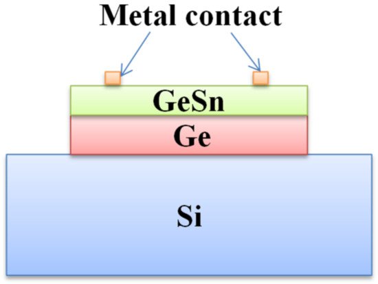
Photoconductive detector, which can also be defined as metal–semiconductor–metal (MSM) detector, is regarded as the simplest structure to achieve detection. In this type of structure, two Schottky junctions are designed and the total layer structure does not require any doping. Therefore, it can only work at a high bias voltage due to the existence of high contact resistance. However, the capacitance of a photoconductive detector is quite low, which is helpful for high-speed detection. Based on the photoconductive structure, researchers have put great effort into GeSn photoconductive detectors ( Figure 1 ). Table 1 shows the reported performance levels of GeSn photoconductive detectors grown by CVD technology.
| Year | Sn Composition | GeSn Thickness | Structure | Cutoff | Responsivity | Ref. |
|---|---|---|---|---|---|---|
| 2012 | 9% | 13 or 20 nm | GeSn/Ge 3QWs | 2200 nm | 0.1 A/W at 5 V | [73] |
| 2014 | 0.9% | 327 nm | Bulk | 1800 nm | —— | [74] |
In 2019, Huong Tran et al. reported a GeSn photoconductor with high Sn contents (the maximum Sn contents of the top GeSn layer were 12.5%, 15.9%, 15.7%, 17.9%, 20%, and 22.3%) [77]. As the Sn content increased, the cutoff wavelength shifted toward longer wavelength due to the bandgap shrinkage. From 77 to 300 K, the cutoff wavelengths were 3200–3650 nm for the GeSn photoconductor with 22.3% Sn. It is worth noting that this D* value was superior to that of a PbSe detector at the given wavelength range and was comparable to that of a commercial extended-InGaAs detector (4 × 10 10 cm·Hz 1/2 ·W −1 ) at the same wavelength range ( Figure 18 ). Even at 300 K, the passivated device showed better results D* than the PbSe detector from 1500 to 2200 nm.
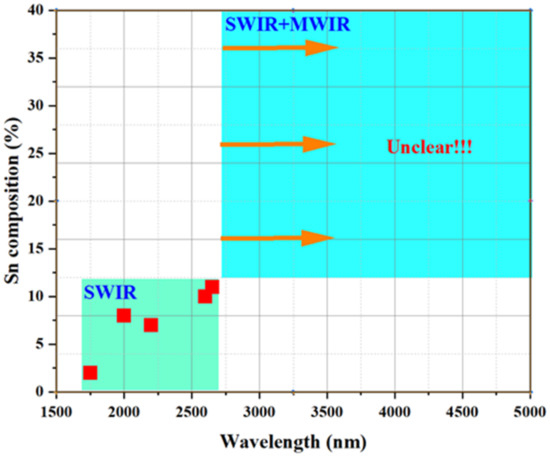
To enable a comprehensive overview of the use of GeSn photoconductive materials for infrared detection applications, Figure 19 illustrates the Sn content vs. cutoff wavelength for reported GeSn photoconductive detectors. For GeSn with an Sn incorporation of 0.9–12.5%, the photoconductive detector wavelength coverage was found to range from 1800 to 2950 nm, indicating that GeSn with Sn contents of up to 12.5% or 13% is very promising for SWIR applications. For GeSn with an Sn incorporation of 15.9–22.3%, the photoconductive detector wavelength coverage was found to range from 3200 to 3650 nm, suggesting potential mid wavelength infrared (MWIR) applications. For wavelengths from 3650 to 5000 nm, no detectors have been reported. However, GeSn photoconductive detector performance is limited by current growth technology and Sn distribution uniformity in total layer structures, which causes a low responsivity (the responsivity values are listed in the table above).
Figure 2 summarize the Sn content vs. cut-off wavelength for a reported GeSn PIN detector. For GeSn with an Sn incorporation of 2–11%, the PIN detector wavelength coverage was found to range from 1750 to 2650 nm, indicating that a GeSn PIN detector is very promising for SWIR applications. Due to the limitations of growth technology, PIN detectors at wavelengths from 2650 to 5000 nm have yet to be reported.
3. Research Progress for GeSn Lasers
Since Si-based high-efficiency light sources comprise the technical bottleneck for Si-based monolithic optoelectronic integration, researchers have conducted extensive research into Ge and GeSn lasers. Ten years ago, the rapid development of the GeSn CVD growth technique enabled researchers from MIT to demonstrate optically injected and electrically injected Ge lasers at room temperature. The lasing thresholds of these laser devices were very high, which made it difficult to achieve efficient lasing. As a result, more attentions has been paid to the GeSn material due to its direct bandgap property. In this section, we review the latest research on GeSn lasers with different optical cavities, as well as their device performance.
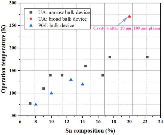
The simplest optical cavity is that of Fabry–Pérot, which consists of two parallel reflecting surfaces that allow coherent light to travel through the whole cavity. Due to the directness difference between GeSn alloys with different contents, we summarize the reported operation temperatures for GeSn with different Sn contents in Figure 3 . Operation temperatures were found to increase with more Sn incorporation, indicating that operation temperature is closely related to the directness of GeSn. Different from narrow bulk devices, broad bulk devices (with a cavity width greater than 20 μm) possess higher operation temperatures, possibly due to the following two reasons: (1) they have higher optical gains, and (2) they are wider and thus have higher optical injection efficiencies. However, the operation temperature for a GeSn laser with 22.3% Sn incorporation was found to be the same as that of a GeSn laser with 17.5% Sn incorporation, which means that there were many point defects in the high-Sn-content GeSn layer. For clarification, we also summarize the devices performance for the published FP cavity optically pumped GeSn laser ( Table 2 ).
| Year | Structure | Sn (%) | Thickness (nm) | Cavity Width (μm) | Pumping | T | max | (K) | Threshold (kW/cm | 2 | ) | Ref |
|---|---|---|---|---|---|---|---|---|---|---|---|---|
| 2015 | Bulk | 12.6 | 560 | 5 | Pulsed 1064 nm | 90 | 1000 at 90 K 325 at 20 K |
[33] | ||||
| 2016 | Hetero | 11 | 260 and 760 | 5 | Pulsed 1064 nm | 110 | 68 at 10 K 166 at 90 K 398 at 110 K |
[34] | ||||
| 3.2% | 76 nm | 1900 nm | —— | |||||||||
| 2017 | Bulk | 7.3 | 210 and 680 | 5 | Pulsed 1064 nm | 77 | 300 at 77 K | [36] | 7.0% | 240 nm | 2100 nm | |
| 9.9 | 280 and 850 | 0.18 A/W at 10 V | ||||||||||
| 140 | 117 at 77 K | 2014 | 10% | 95 nm | Bulk | 2400 nm | 1.63 A/W at 50 V | |||||
| 11.4 | 180 and 660 | [ | 75 | 140 | ] | |||||||
| 160 at 77 K | 2015 | 10% | 95 nm | Bulk | 2400 nm | 0.26 A/W | [76] | |||||
| 14.4 | 250 and 670 | 2019 | 12.5% | 140 and 660 nm | Bulk | 2950 nm | 2 A/W | [77] | ||||
| 160 | 138 at 77 K | |||||||||||
| 15.9 | 210 and 450 | 77 | 267 at 77 K | 15.9% | 250 and 670 nm | 3200 nm | 0.044 A/W | |||||
| 16.6 | 160, 680, and 290 | 140 | 150 at 77 K | 15.7% | 165, 585, and 254 nm | 3400 nm | 0.0072 A/W | |||||
| 17.8 | 310, 550, and 260 | 180 | 171 at 77 K | 17.9% | 310, 550, and 260 nm | 3350 nm | 0.0038 A/W | |||||
| 2018 | Bulk | 22.3 | 380 and 830 | 5 | Pulsed 1064 nm | 150 | 203 at 77 K 609 at 150 K |
[38] | 20% | 450 and 950 nm | 3650 nm | 0.0067 A/W |
| Pulsed 1950 nm | 180 | 137 at 77 K | 22.3% | 380 and 830 nm | 3650 nm | 0.0032 A/W | ||||||
| 2018 | QWs | 13.8 | 22 (4×) | —— | Pulsed 1950 nm | 20 | —— | [46] | ||||
| 14.4 | 31 (4×) | —— | 90 | 25 at 10 K 480 at 90 K |
||||||||
| 2019 | Bulk | 20 | 450 and 970 | 5 | Pulsed 1064 nm | 120 | 516 at 77 K | [39] | ||||
| 20 | 260 | 384 at 77 K | ||||||||||
| 100 | 260 | 356 at 77 K | ||||||||||
| planar | 260 | 330 at 77 K | ||||||||||
| 5 | Pulsed 1950 nm | 140 | 132 at 77 K | |||||||||
| 20 | 270 | 88 at 77 K | ||||||||||
| 100 | 270 | 47 at 77 K | ||||||||||
| planar | 270 | 74 at 77 K |
In 2020, Anas Elbaz et al. created an optically injected GeSn microdisk laser after proper defect management [44][45], indicating that the threshold was greatly reduced compared to that of a GeSn microdisk laser without defect management (the lasing threshold reduction was 1 order of magnitude higher compared to examples in the literature). They also found that the maximum lasing temperature for the optically injected GeSn microdisk laser, with Sn contents ranging from 7% to 10.5%, only weakly depended on Sn content. Apart from the directness of the GeSn active region, the experimental results indicated that nonradiative recombinations and point defects are the main obstacles for high-temperature lasing. The abovementioned GeSn microdisk laser results show that both pulsed and CW injection have been achieved ( . Especially for CW lasing, this is the most direct evidence to verify that GeSn can withstand a CW injection test. To gain a better understanding of GeSn microdisk lasers, we summarize the operation temperatures for GeSn lasers with different Sn contents in Figure 3. For the pulsed injection, the operation temperature for the GeSn microdisk laser followed a similar trend to that of an FP cavity GeSn laser (the operation temperature increased with Sn content). However, the operation temperature for the heterostructure and quantum well GeSn laser was lower than that of bulk laser, suggesting that there is still room to improve the operation temperatures of heterostructure and quantum well lasers. For CW injection, it seems that operation temperature enhancement is not that sensitive to Sn content, though it brings efficient heat dissipation.
4. GeSn Transistors
In addition to the rapid advancement of GeSn detectors and GeSn lasers grown by CVD technology, there have been some achievements in the field of GeSn transistors due to their mobility properties. In the hyper-scaling era, the quest for high-performance and low-power transistors is continuing and intensifying. One of the key technology enablers of these goals is that of channel materials with high carrier mobility and direct band gap structures [78][79]. GeSn films have emerged as the most promising candidate for next generation nano-electronic devices of computing due to their excellent properties, including ultrahigh hole mobility, band structures with direct and low band gaps, Si-based CMOS compatibility, and low thermal budget, all of which are of great importance for ultrahigh density devices and 3D integration in the hyper-scaling era. Anisotropy at the top of the GeSn valence band makes the effective mass of light hole rapidly decrease with increases of Sn content and the transport capacity rapidly increase. GeSn is a very promising channel material for the next generation pMOSFET, and its hole mobility is even higher than that of Ge. The hole mobility of Ge pMOSFET is increased by more than 10 times with respect to Si devices. In addition, compressive strain can improve the mobility of a GeSn channel by decreasing the effective mass of the hole carrier. GeSn is generally grown on Si substrates using Ge as the buffer layer, and GeSn subjects the Ge buffer layer to compressive strain since the Sn lattice constant is greater than that of Ge. As GeSn materials are compatible with Si-CMOS technology, a few research groups have studied GeSn-based transistors ( Table 3 lists the reported transistors with CVD-grown GeSn layers).
| Year | Institution | Transistor Type | Sn Composition (%) | SS (mV/dec) | I | on | /I | off | V | DS | (V) | Refs |
|---|---|---|---|---|---|---|---|---|---|---|---|---|
| 2017 | University of Notre Dame | Ge/GeSn p-type TFETs | 11 and 12.5 | 215 | 9.2 × 10 | 3 | −0.5 | [80] | ||||
| 2017 | NUS | GeSn FinFET on GeSnOI | 8 | 79 | >10 | 4 | −0.5 | [81] | ||||
| 2017 | National Taiwan University | Vertically Stacked GeSn Nanowire pGAAFETs | 6 and 10 | 84 | —— | −1 | [82] | |||||
| 2017 | National Taiwan University | GeSn N-FinFETs | 8 | 138 | 10 | 3 | —— | [83] | ||||
| 2018 | National Taiwan University | GeSn N-Channel MOSFETs | 4.5 | 180 | —— | —— | [84] | |||||
| 2018 | National Taiwan University | Vertically Stacked 3-GeSn- Nanosheet pGAAFETs | 7 | 108 | 5 × 10 | 3 | −0.5 | [85] | ||||
| 2020 | PGI 9 | Vertical heterojunction GeSn/Ge gate-all-around nanowire pMOSFETs | 8 | 130 | 3 × 10 | 6 | −0.5 | [86] |
Tunnel-field-effect transistors (TFETs) features subthreshold swings (SS) below 60 mV/decade at room temperature, which also enable a decreased power supply without discounting the off-current. Although Si-TFETs have been reported with SS below 60 mV/decade at low current, band-to-band tunneling (BTBT) is limited by its indirect bandgap property and low SS at high current. Therefore, researchers have investigated GeSn with high Sn contents to create high-performance GeSn TFETs [87]. A higher Sn content enhances device performance, but the subthreshold swing is affected by the increased leakage level. For ultrasmall supply voltages, the device structure should be optimized to improve device characteristics. Using Ge/GeSn heterostructure pTFETs led to the improvements of the BTBT rate. Thus, higher on-current and lower off-current were achieved simultaneously. Christian et al. reported the fabrication and characterization of Ge/GeSn pTFETs, and they recorded a low accumulation capacitance of 3 μF/cm 2 [80]. Moreover, their room-temperature (RT) current–voltage characteristics showed that the Ge/GeSn pTFETs with the 11% Sn content had the highest BTBT current. To suppress the short channel effects (SCEs) of multi-gate transistors, Dianlei et al. investigated the p-FinFETs with a CVD-grown GeSn channel [81]. For GeSn p-FinFETs grown on GeSnOI substrates with 8% Sn incorporation, compressive strain and hole mobility were found to be −0.9% and 208 cm 2 /V·s, respectively. Record low SS of 79 mV/decade for GeSn p-FETs were also achieved.
References
- Soref, R. Silicon photonics: A review of recent literature. Silicon 2010, 2, 1–6.
- Paul, D.J. Silicon photonics: A bright future? Electron. Lett. 2009, 45, 582–584.
- Soref, R.A. Silicon-based optoelectronics. Proc. IEEE 1993, 81, 1687–1706.
- Soref, R.; Buca, D.; Yu, S.Q. Group IV photonics: Driving integrated optoelectronics. Opt. Photonics News 2016, 27, 32–39.
- Radamson, H.; Thylén, L. Monolithic Nanoscale Photonics-Electronics Integration in Silicon and Other Group IV Elements; Academic Press: Cambridge, MA, USA, 2014.
- Geiger, R.; Zabel, T.; Sigg, H. Group IV direct band gap photonics: Methods, challenges, and opportunities. Front. Mater. 2015, 2, 52.
- Zhang, L.; Hong, H.; Li, C.; Chen, S.; Huang, W.; Wang, J.; Wang, H. High-Sn fraction GeSn quantum dots for Si-based light source at 1.55 μm. Appl. Phys. Express 2019, 12, 055504.
- Wang, T.; Wei, W.; Feng, Q.; Wang, Z.; Zhang, J. Telecom InAs quantum-dot FP and microdisk lasers epitaxially grown on (111)-faceted SOI. In Proceedings of the 2020 Conference on Lasers and Electro-Optics (CLEO), Washington, DC, USA, 10–15 May 2020; pp. 1–2.
- Wei, W.; Feng, Q.; Wang, Z.; Wang, T.; Zhang, J. Perspective: Optically-pumped III–V quantum dot microcavity lasers via CMOS compatible patterned Si (001) substrates. J. Semicond. 2019, 40, 101303.
- Liu, W.K.; Lubyshev, D.; Fastenau, J.M.; Wu, Y.; Bulsara, M.T.; Fitzgerald, E.A.; Urteaga, M.; Ha, W.; Bergman, J.; Brar, B.; et al. Monolithic integration of InP-based transistors on Si substrates using MBE. J. Cryst. Growth 2009, 311, 1979–1983.
- Liow, T.Y.; Ang, K.W.; Fang, Q.; Song, J.F.; Xiong, Y.Z.; Yu, M.B.; Guo, Q.; Kwong, D.L. Silicon modulators and germanium photodetectors on SOI: Monolithic integration, compatibility, and performance optimization. IEEE J. Sel. Top. Quantum Electron. 2009, 16, 307–315.
- Saito, S.; Al-Attili, A.Z.; Oda, K.; Ishikawa, Y. Towards monolithic integration of germanium light sources on silicon chips. Semicond. Sci. Technol. 2016, 31, 043002.
- Yu, H.Y.; Ren, S.; Jung, W.S.; Okyay, A.K.; Miller, D.A.; Saraswat, K.C. High-efficiency pin photodetectors on selective-area-grown Ge for monolithic integration. IEEE Electron. Device Lett. 2009, 30, 1161–1163.
- González-Fernández, A.A.; Juvert, J.; Aceves-Mijares, M.; Domínguez, C. Monolithic integration of a silicon-based photonic transceiver in a CMOS process. IEEE Photonics J. 2015, 8, 1–13.
- Li, B.; Li, G.; Liu, E.; Jiang, Z.; Pei, C.; Wang, X. 1.55 μm reflection-type optical waveguide switch based on SiGe/Si plasma dispersion effect. Appl. Phys. Lett. 1999, 75, 1–3.
- Zhao, D.; Shi, B.; Jiang, Z.; Fan, Y.; Wang, X. Silicon-based optical waveguide polarizer using photonic band gap. Appl. Phys. Lett. 2002, 81, 409–411.
- Zhao, X.; Wang, G.; Lin, H.; Du, Y.; Luo, X.; Kong, Z.; Su, J.; Li, J.; Xiong, W.; Miao, Y.; et al. High performance pin photodetectors on Ge-on-insulator platform. Nanomaterials 2021, 11, 1125.
- Michel, J.; Liu, J.; Kimerling, L.C. High-performance Ge-on-Si photodetectors. Nat. Photonics 2010, 4, 527–534.
- Lin, T.Y.; Lin, K.T.; Lin, C.C.; Lee, Y.W.; Shiu, L.T.; Chen, W.Y.; Chen, H.L. Magnetic fields affect hot electrons in silicon-based photodetectors at telecommunication wavelengths. Mater. Horiz. 2019, 6, 1156–1168.
- Marris-Morini, D.; Vivien, L.; Rasigade, G.; Fedeli, J.M.; Cassan, E.; Le Roux, X.; Laval, S. Recent progress in high-speed silicon-based optical modulators. Proc. IEEE 2009, 97, 1199–1215.
- Reed, G.T.; Png, C.E.J. Silicon optical modulators. Mater. Today 2005, 8, 40–50.
- Reed, G.T.; Mashanovich, G.; Gardes, F.Y.; Thomson, D.J. Silicon optical modulators. Nat. Photonics 2010, 4, 518–526.
- Haché, A.; Bourgeois, M. Ultrafast all-optical switching in a silicon-based photonic crystal. Appl. Phys. Lett. 2000, 77, 4089–4091.
- Juan, W.H.; Pang, S.W. High-aspect-ratio Si vertical micromirror arrays for optical switching. J. Microelectromech. Syst. 1998, 7, 207–213.
- Fadaly, E.M.; Dijkstra, A.; Suckert, J.R.; Ziss, D.; van Tilburg, M.A.; Mao, C.; Ren, Y.; Lange, V.; Korzun, K.; Bakkers, E.P.; et al. Direct-bandgap emission from hexagonal Ge and SiGe alloys. Nature 2020, 580, 205–209.
- Sukhdeo, D.S.; Nam, D.; Kang, J.H.; Brongersma, M.L.; Saraswat, K.C. Direct bandgap germanium-on-silicon inferred from 5.7% 〈 100〉 uniaxial tensile strain. Photonics Res. 2014, 2, A8–A13.
- Sun, X.; Liu, J.; Kimerling, L.C.; Michel, J. Room-temperature direct bandgap electroluminesence from Ge-on-Si light-emitting diodes. Opt. Lett. 2009, 34, 1198–1200.
- Michel, J.; Camacho-Aguilera, R.E.; Cai, Y.; Patel, N.; Bessette, J.T.; Romagnoli, M.; Kimerling, L.C. An Electrically Pumped Ge-on-Si Laser; OFC/NFOEC; IEEE: New York, NY, USA, 2012; pp. 1–3.
- Camacho-Aguilera, R.E.; Cai, Y.; Patel, N.; Bessette, J.T.; Romagnoli, M.; Kimerling, L.C.; Michel, J. An electrically pumped germanium laser. Opt. Express 2012, 20, 11316–11320.
- Liu, J.; Sun, X.; Camacho-Aguilera, R.; Cai, Y.; Kimerling, L.C.; Michel, J. Optical Gain and Lasing from Band-Engineered Ge-on-Si at Room Temperature; Institute of Electrical and Electronics Engineers (IEEE): New York, NY, USA, 2010.
- Koerner, R.; Oehme, M.; Gollhofer, M.; Schmid, M.; Kostecki, K.; Bechler, S.; Widmann, D.; Kasper, E.; Schulze, J. Electrically pumped lasing from Ge Fabry-Perot resonators on Si. Opt. Express 2015, 11, 14815–14822.
- Ghetmiri, S.A.; Du, W.; Margetis, J.; Mosleh, A.; Cousar, L.; Conley, B.R.; Domulevicz, L.; Nazzal, A.; Sun, G.; Soref, R.A.; et al. Direct-bandgap GeSn grown on silicon with 2230 nm photoluminescence. Appl. Phys. Lett. 2014, 105, 151109.
- Wirths, S.; Geiger, R.; Von Den Driesch, N.; Mussler, G.; Stoica, T.; Mantl, S.; Ikonic, Z.; Luysberg, M.; Buca, D.; Grützmacher, D.; et al. Lasing in direct-bandgap GeSn alloy grown on Si. Nat. Photonics 2015, 9, 88–92.
- Al-Kabi, S.; Ghetmiri, S.A.; Margetis, J.; Pham, T.; Zhou, Y.; Dou, W.; Collier, B.; Quinde, R.; Du, W.; Yu, S.Q.; et al. An optically pumped 2.5 μ m GeSn laser on Si operating at 110 K. Appl. Phys. Lett. 2016, 109, 171105.
- Thai, Q.M.; Pauc, N.; Aubin, J.; Bertrand, M.; Chrétien, J.; Chelnokov, A.; Martmann, J.; Reboud, V.; Calvo, V. 2D hexagonal photonic crystal GeSn laser with 16% Sn content. Appl. Phys. Lett. 2018, 113, 051104.
- Margetis, J.; Al-Kabi, S.; Du, W.; Dou, W.; Zhou, Y.; Pham, T.; Grant, P.; Ghetmiri, S.; Mosleh, A.; Li, B.; et al. Si-based GeSn lasers with wavelength coverage of 2–3 μm and operating temperatures up to 180 K. ACS Photonics 2017, 5, 827–833.
- Stange, D.; Wirths, S.; Geiger, R.; Schulte-Braucks, C.; Marzban, B.; von den Driesch, N.; Mussler, G.; Zabel, T.; Stoica, T.; Buca, D.; et al. Optically pumped GeSn microdisk lasers on Si. ACS Photonics 2016, 3, 1279–1285.
- Dou, W.; Zhou, Y.; Margetis, J.; Ghetmiri, S.A.; Al-Kabi, S.; Du, W.; Liu, J.; Sun, G.; Soref, R.; Yu, S.Q.; et al. Optically pumped lasing at 3 μm from compositionally graded GeSn with tin up to 22.3%. Opt. Lett. 2018, 43, 4558–4561.
- Zhou, Y.; Dou, W.; Du, W.; Ojo, S.; Tran, H.; Ghetmiri, S.A.; Liu, J.; Sun, G.; Soref, R.; Yu, S.Q.; et al. Optically pumped GeSn lasers operating at 270 K with broad waveguide structures on Si. ACS Photonics 2019, 6, 1434–1441.
- Chrétien, J.; Pauc, N.; Armand Pilon, F.; Bertrand, M.; Thai, Q.M.; Casiez, L.; Bernier, N.; Dansas, H.; Gergaud, P.; Hartmann, J.; et al. GeSn lasers covering a wide wavelength range thanks to uniaxial tensile strain. ACS Photonics 2019, 6, 2462–2469.
- Reboud, V.; Gassenq, A.; Pauc, N.; Aubin, J.; Milord, L.; Thai, Q.M.; Bertrand, M.; Guilloy, K.; Rouchon, D.; Calvo, V.; et al. Optically pumped GeSn micro-disks with 16% Sn lasing at 3.1 μm up to 180 K. Appl. Phys. Lett. 2017, 111, 092101.
- Du, W.; Thai, Q.M.; Chrétien, J.; Bertrand, M.; Casiez, L.; Zhou, Y.; Margetis, J.; Pauc, N.; Reboud, V.; Yu, S.Q.; et al. Study of Si-based GeSn optically pumped lasers with micro-disk and ridge waveguide structures. Front. Phys. 2019, 7, 147.
- Elbaz, A.; Buca, D.; von den Driesch, N.; Pantzas, K.; Patriarche, G.; Zerounian, N.; Herth, E.; Checory, X.; Sauvage, S.; El Kurdi, M.; et al. Ultra-low-threshold continuous-wave and pulsed lasing in tensile-strained GeSn alloys. Nat. Photonics 2020, 14, 375–382.
- Kurdi, M.E.; Elbaz, A.; Wang, B.; Sakat, E.; Herth, E.; Patriarche, G.; Pantzas, K.; Sagnes, I.; Sauvage, S.; Buca, D. Tensile Strain Engineering and Defects Management in GeSn Laser Cavities. ECS Trans. 2020, 98, 61.
- Elbaz, A.; Arefin, R.; Sakat, E.; Wang, B.; Herth, E.; Patriarche, G.; Foti, A.; Ossikovski, R.; Sauvage, S.; Checoury, X.; et al. Reduced lasing thresholds in GeSn microdisk cavities with defect management of the optically active region. ACS Photonics 2020, 7, 2713–2722.
- Margetis, J.; Zhou, Y.; Dou, W.; Grant, P.C.; Alharthi, B.; Du, W.; Tran, H.; Ojo, S.; Liu, J.; Yu, S.Q.; et al. All group-IV SiGeSn/GeSn/SiGeSn QW laser on Si operating up to 90 K. Appl. Phys. Lett. 2018, 113, 221104.
- Stange, D.; von den Driesch, N.; Zabel, T.; Armand-Pilon, F.; Rainko, D.; Marzban, B.; Zaumseil, P.; Hartmann, J.M.; Ikonic, Z.; Buca, D.; et al. GeSn/SiGeSn heterostructure and multi quantum well lasers. ACS Photonics 2018, 5, 4628–4636.
- Thai, Q.M.; Pauc, N.; Aubin, J.; Bertrand, M.; Chrétien, J.; Delaye, V.; Chelnokov, A.; Hartmann, J.; Reboud, V.; Calvo, V. GeSn heterostructure micro-disk laser operating at 230 K. Opt. Express 2018, 26, 32500–32508.
- Von den Driesch, N.; Stange, D.; Rainko, D.; Povstugar, I.; Zaumseil, P.; Capellini, G.; Denneulin, T.; Ikonic, Z.; Hartmann, J.; Buca, D.; et al. Advanced GeSn/SiGeSn group IV heterostructure lasers. Adv. Sci. 2018, 5, 1700955.
- Fujisawa, T.; Arai, M.; Saitoh, K. Microscopic gain analysis of modulation-doped GeSn/SiGeSn quantum wells: Epitaxial design toward high-temperature lasing. Opt. Express 2019, 27, 2457–2464.
- Dou, W.; Benamara, M.; Mosleh, A.; Margetis, J.; Grant, P.; Zhou, Y.; Al-Kabi, S.; Du, W.; Tolle, J.; Yu, S.Q.; et al. Investigation of GeSn strain relaxation and spontaneous composition gradient for low-defect and high-Sn alloy growth. Sci. Rep. 2018, 8, 1–11.
- Zhou, Y.; Miao, Y.; Ojo, S.; Tran, H.; Abernathy, G.; Grant, J.M.; Amoah, S.; Salamo, G.; Du, W.; Yu, S.Q.; et al. Electrically injected GeSn lasers on Si operating up to 100 K. Optica 2020, 7, 924–928.
- Zhou, Y.; Ojo, S.; Miao, Y.; Tran, H.; Grant, J.M.; Abernathy, G.; Amoah, S.; Bass, J.; Salamo, G.; Yu, S.Q.; et al. Electrically injected GeSn lasers with peak wavelength up to 2.7 micrometer at 90 K. arXiv Preprint 2020, arXiv:2009.12229.
- Mosleh, A.; Alher, M.; Cousar, L.C.; Du, W.; Ghetmiri, S.A.; Al-Kabi, S.; Dou, W.; Sun, G.; Soref, R.; Yu, S.Q.; et al. Buffer-free GeSn and SiGeSn growth on Si substrate using in situ SnD4 gas mixing. J. Electron. Mater. 2016, 45, 2051–2058.
- Grant, P.C.; Dou, W.; Alharthi, B.; Grant, J.M.; Tran, H.; Abernathy, G.; Mosleh, A.; Du, W.; Li, B.; Yu, S.Q.; et al. UHV-CVD growth of high quality GeSn using SnCl4: From material growth development to prototype devices. Opt. Mater. Express 2019, 9, 3277–3291.
- Cook, C.S.; Zollner, S.; Bauer, M.R.; Aella, P.; Kouvetakis, J.; Menendez, J. Optical constants and interband transitions of Ge1− xSnx alloys (x < 0.2) grown on Si by UHV-CVD. Thin Solid Film. 2004, 455, 217–221.
- Xu, C.; Gallagher, J.; Senaratne, C.; Brown, C.; Fernando, N.; Zollner, S.; Kouvetakis, J.; Menendez, J. Doping and strain dependence of the electronic band structure in Ge and GeSn alloys. In APS March Meeting Abstracts; American Physical Society: College Park, MD, USA, 2015.
- Margetis, J.; Mosleh, A.; Ghetmiri, S.A.; Al-Kabi, S.; Dou, W.; Du, W.; Bhargava, N.; Yu, S.; Profijt, H.; Tolle, J.; et al. Fundamentals of Ge1−xSnx and SiyGe1−x−ySnx RPCVD epitaxy. Mater. Sci. Semicond. Process. 2017, 70, 38–43.
- Margetis, J.; Ghetmiri, S.A.; Du, W.; Conley, B.R.; Mosleh, A.; Soref, R.; Yu, S.; Tolle, J. Growth and characterization of epitaxial Ge1-XSnx alloys and heterostructures using a commercial CVD system. ECS Tran. 2014, 64, 711.
- Chen, R.; Huang, Y.C.; Gupta, S.; Lin, A.C.; Sanchez, E.; Kim, Y.; Saraswat, K.; Kamins, T.; Harris, J.S. Material characterization of high Sn-content, compressively-strained GeSn epitaxial films after rapid thermal processing. J. Crys. Growth 2013, 365, 29–34.
- Wirths, S.; Buca, D.; Mussler, G.; Tiedemann, A.T.; Holländer, B.; Bernardy, P.; Stoica, T.; Grutzmacher, D.; Mantl, S. Reduced pressure CVD growth of Ge and Ge1−xSnx alloys. ECS J. Solid State Sci. Tech. 2013, 2, N99.
- Zhang, L.; Chen, Q.; Wu, S.; Son, B.; Lee, K.H.; Chong, G.Y.; Tan, C.S. Growth and Characterizations of GeSn Films with High Sn Composition by Chemical Vapor Deposition (CVD) Using Ge2H6 and SnCl4 for Mid-IR Applications. ECS Trans. 2020, 98, 91.
- Kohen, D.; Vohra, A.; Loo, R.; Vandervorst, W.; Bhargava, N.; Margetis, J.; Tolle, J. Enhanced B doping in CVD-grown GeSn: B using B δ-doping layers. J. Crys. Growth 2018, 483, 285–290.
- Vanjaria, J.; Arjunan, A.C.; Salagaj, T.; Tompa, G.S.; Yu, H. PECVD Growth of Composition Graded SiGeSn Thin Films as Novel Approach to Limit Tin Segregation. ECS J. Solid State Sci. Tech. 2020, 9, 034009.
- Vanjaria, J.V. Growth and Characterization of Si-Ge-Sn Semiconductor Thin Films using a Simplified PECVD Reactor. Ph.D. Thesis, Arizona State University, Tempe, AZ, USA, 2020.
- Dou, W.; Alharthi, B.; Grant, P.C.; Grant, J.M.; Mosleh, A.; Tran, H.; Du, W.; Li, B.; Naseem, H.; Yu, S.Q.; et al. Crystalline GeSn growth by plasma enhanced chemical vapor deposition. Opt. Mater. Express 2018, 8, 3220–3229.
- Li, Z. Room Temperature Lasing in GeSn Alloys. Ph.D. Thesis, University of Dayton, Dayton, OH, USA, 2015.
- Assali, S.; Nicolas, J.; Mukherjee, S.; Dijkstra, A.; Moutanabbir, O. Atomically uniform Sn-rich GeSn semiconductors with 3.0–3.5 μm room-temperature optical emission. Appl. Phys. Lett. 2018, 112, 251903.
- Assali, S.; Nicolas, J.; Moutanabbir, O. Enhanced Sn incorporation in GeSn epitaxial semiconductors via strain relaxation. J. Appl. Phys. 2019, 125, 025304.
- Assali, S.; Attiaoui, A.; Del Vecchio, P.; Mukherjee, S.; Kumar, A.; Moutanabbir, O. Epitaxial growth of atomically-sharp GeSn/Ge/GeSn tensile strained (≥1.5%) quantum well on Si. Bull. Am. Phys. Soc. 2020, 65, 6.
- Gupta, S.; Chen, R.; Vincent, B.; Lin, D.; Magyari-Kope, B.; Caymax, M.; Dekoster, J.; Harris, J.; Nishi, Y.; Saraswat, K.C. GeSn channel n and p MOSFETs. ECS Trans. 2013, 50, 937.
- Loo, R.; Shimura, Y.; Ike, S.; Vohra, A.; Stoica, T.; Stange, D.; Buca, D.; Kohen, D.; Margetis, J.; Tolle, J. Epitaxial GeSn: Impact of process conditions on material quality. Semicond. Sci. Technol. 2018, 33, 114010.
- Gassenq, A.; Gencarelli, F.; Van Campenhout, J.; Shimura, Y.; Loo, R.; Narcy, G.; Vincent, B.; Roelkens, G. GeSn/Ge heterostructure short-wave infrared photodetectors on silicon. Opt. Express 2012, 20, 27297–27303.
- Conley, B.R.; Margetis, J.; Du, W.; Tran, H.; Mosleh, A.; Ghetmiri, S.A.; Tolle, J.; Sun, G.; Soref, R.; Li, B.; et al. Si based GeSn photoconductors with a 1.63 A/W peak responsivity and a 2.4 μm long-wavelength cutoff. Appl. Phys. Lett. 2014, 105, 221117.
- Conley, B.R.; Mosleh, A.; Ghetmiri, S.A.; Du, W.; Soref, R.A.; Sun, G.; Margetis, J.; Tolle, J.; Nassem, H.; Yu, S.Q. Temperature dependent spectral response and detectivity of GeSn photoconductors on silicon for short wave infrared detection. Opt. Express 2014, 22, 15639–15652.
- Pham, T.N.; Du, W.; Conley, B.R.; Margetis, J.; Sun, G.; Soref, R.A.; Tolle, J.; Li, B.; Yu, S.Q. Si-based Ge0.9Sn0.1 photodetector with peak responsivity of 2.85 A/W and longwave cutoff at 2.4 μm. Electron. Lett. 2015, 51, 854–856.
- Tran, H.; Pham, T.; Margetis, J.; Zhou, Y.; Dou, W.; Grant, P.C.; Grant, J.; Sun, G.; Tolle, J.; Du, W.; et al. Si-based GeSn photodetectors toward mid-infrared imaging applications. ACS Photonics 2019, 6, 2807–2815.
- Radamson, H.H.; Luo, J.; Simoen, E.; Zhao, C. CMOS Past, Present and Future; Woodhead Publishing: Cambridge, UK, 2018; ISBN 9780081021392.
- Takagi, S.; Iisawa, T.; Tezuka, T.; Numata, T.; Nakaharai, S.; Hirashita, N.; Moriyama, Y.; Usuda, K.; Toyoda, E.; Sugiyama, N.; et al. Carrier-transport-enhanced channel CMOS for improved power consumption and performance. IEEE Trans. Electron Devices 2007, 55, 21–39.
- Schulte-Braucks, C.; Pandey, R.; Sajjad, R.N.; Barth, M.; Ghosh, R.K.; Grisafe, B.; Loo, R.; Mantl, S.; Buca, D.; Datta, S.; et al. Fabrication, characterization, and analysis of Ge/GeSn heterojunction p-type tunnel transistors. IEEE Trans. Electron Devices 2017, 64, 4354–4362.
- Lei, D.; Lee, K.H.; Huang, Y.C.; Wang, W.; Masudy-Panah, S.; Yadav, S.; Kumar, A.; Dong, Y.; Kang, Y.; Yeo, Y.C.; et al. Germanium-tin (GeSn) P-channel fin field-effect transistor fabricated on a novel GeSn-on-insulator substrate. IEEE Trans. Electron Devices 2018, 65, 3754–3761.
- Huang, Y.S.; Lu, F.L.; Tsou, Y.J.; Tsai, C.E.; Lin, C.Y.; Huang, C.H.; Liu, C.W. First vertically stacked GeSn nanowire pGAAFETs with I on = 1850 μA/μm (Vov = Vds = −1 V) on Si by GeSn/Ge CVD epitaxial growth and optimum selective etching. In Proceedings of the 2017 IEEE International Electron Devices Meeting (IEDM), San Francisco, CA, USA, 2–6 December 2017; pp. 1–4.
- Gupta, S.; Vincent, B.; Yang, B.; Lin, D.; Gencarelli, F.; Lin, J.Y.; Chen, R.; Richard, O.; Bender, H.; Saraswat, K.C.; et al. Towards high mobility GeSn channel nMOSFETs: Improved surface passivation using novel ozone oxidation method. In Proceedings of the 2012 International Electron Devices Meeting, San Francisco, CA, USA, 10–13 December 2012; pp. 16.2.1–16.2.4.
- Chuang, Y.; Liu, C.Y.; Luo, G.L.; Li, J.Y. Electron Mobility Enhancement in GeSn n-Channel MOSFETs by Tensile Strain. IEEE Electron. Device Lett. 2020, 42, 10–13.
- Huang, Y.S.; Lu, F.L.; Tsou, Y.J.; Ye, H.Y.; Lin, S.Y.; Huang, W.H.; Liu, C.W. Vertically stacked strained 3-GeSn-nanosheet pGAAFETs on Si using GeSn/Ge CVD epitaxial growth and the optimum selective channel release process. IEEE Electron Device Lett. 2018, 39, 1274–1277.
- Liu, M.; Mertens, K.; von den Driesch, N.; Schlykow, V.; Grap, T.; Lentz, F.; Trellenkamp, S.; Hartmann, J.; Knoch, J.; Buca, D.; et al. Vertical heterojunction Ge0. 92Sn0. 08/Ge gate-all-around nanowire pMOSFETs with NiGeSn contact. Solid-State Electron. 2020, 168, 107716.
- Liu, L.; Liang, R.; Wang, G.; Radamson, H.H.; Wang, J.; Xu, J. Investigation on direct-gap GeSn alloys for high-performance tunneling field-effect transistor applications. In Proceedings of the 2017 IEEE Electron Devices Technology and Manufacturing Conference (EDTM), Toyama, Japan, 28 February–2 March 2017; pp. 180–181.