Your browser does not fully support modern features. Please upgrade for a smoother experience.
Please note this is a comparison between Version 1 by Tetsuya Kawanishi and Version 2 by Bruce Ren.
Optoelectronic devices which play important roles in high-speed optical fiber networks can offer effective measurement methods for optoelectronic devices including optical modulators and photodetectors. Precise optical signal modulation is required for measurement applications.
- optical modulation
- extinction ratio
- chirp parameter
- two-tone signal
- single sideband
- frequency sweep
- electro-optic effect
- optoelectronic devices
Note: The following contents are extract from your paper. The entry will be online only after author check and submit it.
1. Introduction
For high-speed optical links, external modulators are commonly used to generate broadband optical signals. High-speed modulation whose operation bandwidth is up to 100 GHz has been reported by using optical modulators based on electro-optic effect in various materials such as lithium niobate [1][2][1,2], silicon [3][4][3,4] and indium phosphide [5][6][5,6]. Optical signals generated by optical transmitters consisting of lasers and modulators would be converted into electric signals by photodetectors at receivers. Recently, various multilevel modulation techniques have been investigated to increase transmission capacity, where high-speed and precise lightwave control is required in optical-to-electric and electric-to-optical signal conversion [1]. Waveform transfer is needed to construct mobile networks consisting of many base stations and remote antenna units [7]. Waveforms are sent from base stations to remote antenna units over optical fiber links, where waveforms for radio services are generated and processed at base stations [8]. In the fourth generation (4G) mobile system, digital radio-over-fiber (RoF) is commonly used for the waveform transfer, because the required bitrate for digitized waveforms is much less than 10 Gb/s. Thus, we can use low-cost digital optical fiber links for connection between base stations and remote antenna units. However, in the fifth generation (5G) mobile system, the required bitrate for such connection would be larger than a few hundred Gb/s. Analog RoF links would be useful in 5G or beyond mobile systems, to save the required bitrate or bandwidth [8]. Precise lightwave control is required in analog RoF systems, which would be sensitive to nonlinearity and frequency response, as well as in digital transmission systems with multilevel modulation formats.
2. Intensity Modulation by a Balanced Mach-Zehnder Modulator
An MZM consists of two optical phase modulators (PMs) connected in parallel through two Y-junctions, as shown in Figure 1. The two optical paths along the phase modulators form two arms of a Mach-Zehnder interferometer (MZI). Optical phase difference between optical signals on the two optical paths can be controlled through voltages were applied to the two optical PMs (PM and PM2). In an ideal MZM where the amplitudes of the two optical signals are balanced, the optical output intensity goes to zero when the optical phase difference is equal to π (180-degree).
Figure 1. MZM structure.
at a particular frequnecy [9][10]. However, for broadband operation, it would be rather difficult to maintain the balanced operation due to frequency response difference between the two electric circuits for the two electrodes, where the electric circuits to drive the dual-electrode MZM would be more complicated than that of the x-cut single-drive MZM which has only one electrode.
3. Active Trimming for High Extinction-Ratio Intensity Modulation
An MZM with a minimum transmission bias point can generate an optical two-tone signal consisting of the first order USB and LSB, which is useful for measurement applications. Spurious suppression ratio largely depends on the ER. Thus, firstly, we consider enhanement of the ER by active trimming, while the chirp parameter and ER should be adjusted simultaneously, to generate a pure optical two-tone signal.
An integrated x-cut LiNbO3
(LN) modulator with active trimmers can offer high ER intensity modulation [10][9]. As shown in Figure 2, the modulator has a pair of sub MZIs in a main MZI. The sub MZIs compensate imbalance in the main MZI due to fabrication error. The integrated LN modulator has three electrodes (A, B and C). The amplitude balance between the two arms in the main MZI, can be controlled by changing dc-bias voltages fed to the electrodes A and B. A modulation signal on the electrode C controls the optical phase difference between the two arms of the main MZI.
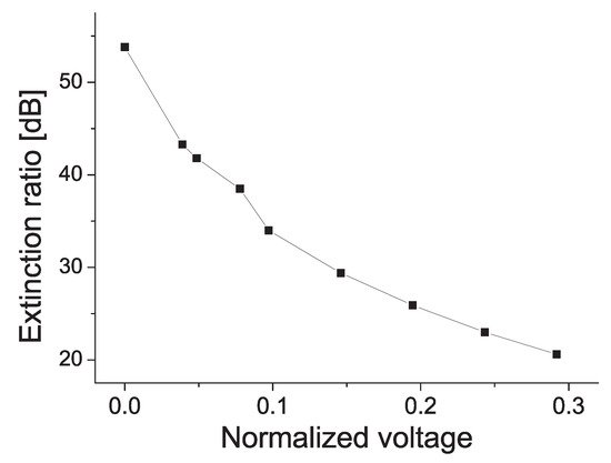
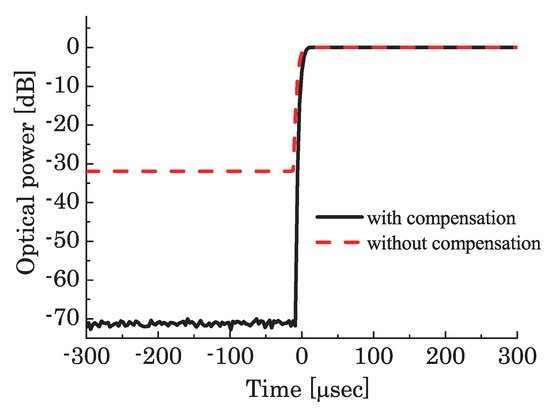
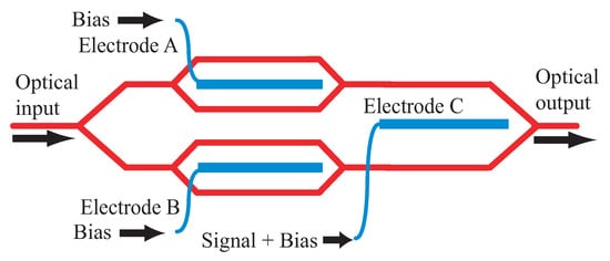 Figure 3 shows time-domain responses of the modulator, where the ERs with and without compensation were, respectively, 71 dB and 32 dB. Zero span operation of an optical spectrum analyzer was used to measure high extinction ratio on-off-keying. The rise and fall times of the time-domain profiles shown in Figure 3 were dominated by the response of the optical spectrum analyzer. Due to fabrication error, optical power in one arm of the MZM should be larger than that in the other arm. The optical power in the arm whose optical loss is larger than in the other arm should be adjusted by using a sub MZI [1]. As shown in Figure 4, the ER can be controlled by the voltage applied to the sub MZI embedded in the arm whose optical loss is larger than the other arm. The x-axis shows the dc-bias voltage offset from the imbalance compensated condition, where the scale was normalized by Vπ
of the sub MZI. The ER-tuning range was from 21 dB to 54 dB.
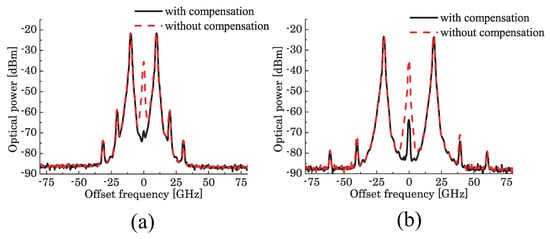
 An MZM with minimum transmission bias can offer double sideband suppressed carrier (DSB-SC) modulation, where the carrier component is suppressed by destructive interference between optical waves propagating in the two waveguides of the main MZI. By feeding a sinusoidal single-tone signal as a modulating signal, we can generate an optical two-tone signal consisting of the first order USB and LSB with suppressed carrier. The suppression ratio depends on the imbalance between the optical waves, in other words, the ER of the modulator. Figure 5 shows optical spectra of optical two-tone signals generated by an MZM with active trimmers. The ER can be higher than 60 dB. The modulating signal frequencies fm
were 10.5 GHz and 20.0 GHz. The main MZI wase set to be a minimum transmission bias condition. Carrier suppression ratios with respect to the first order USB or LSB were 47.4 dB for 10.5 GHz and 40.4 dB for 20.0 GHz, when the ER was enhanced by imbalance conpensation using the active trimmers. On the other hand the suppression ratios without compensation were less than 20 dB.
 Parasitic optical phase modulation due to imbalance in induced phases on the two arms in the main MZI also causes generation of undesired high order sidebands. Such imbalance can be described by a chirp parameter [1]. The second order sideband generation was mainly due to the parasitic optical phase modulation associated with the chirp parameter α
, while the third order components are due to intrinsic nonlinearity of the MZMs. As described above, the chirp parameter α
can be largely suppressed by using a dual-electrode MZM [9][10].
By using a high-speed photodetector, the optical two-tone signal can be converted into a pure single-tone electric signal as a beat signal of the two optical spectral components whose frequency separation is equal to 2fm
. Figure 6a,b show wide span (DC-50 GHz) spectra of the RF signal generated from the optical two-tone signal (fm=20.0GHz
). with and without the compensation technique, respectively, where resolution bandwidth was 43 kHz. By using active trimming, the spurious suppression ratio could be larger than 60 dB without using any electrical or optical filters for suppression of undesired components, where the suppression ratio without using active trimming was 21.0 dB. The linewidth of the generated millimeter-wave signal was almost equal to that of the modulating signal.
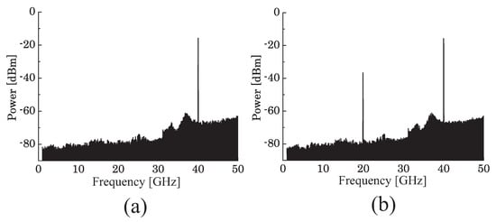

Figure 2. Integrated MZM with two active trimmers.


Figure 5. Spectra of optical two-tone signals with fm

Figure 6. Spectra of RF signals generated from optical two-tone signals with compensation (a) and without compensation (b) [1].

