Two-dimensional (2D) materials are defined as crystalline materials consisting of single- or few-layer atoms, in which the in-plane interatomic interactions are much stronger than those along the stacking direction. Since the success of monolayer graphene exfoliation, 2D materials have been extensively studied due to their unique structures and unprecedented properties. Among these fascinating studies, the most predominant focus has been on their atomic structures, defects, and mechanical behaviors and properties, which serve as the basis for the practical applications of 2D materials.
- two-dimensional materials
- mechanical behaviors
- mechanical properties
- structural defects
- heterostructures
1. Introduction
Two-dimensional (2D) materials are defined as crystalline materials consisting of single- or few-layer atoms, in which the in-plane interatomic interactions are much stronger than those along the stacking direction. Since the first exfoliation of single-layer graphene [1], 2D materials have attracted worldwide attention due to their unique structures and remarkable properties [2,3,4,5,6,7][2][3][4][5][6][7]. For example, graphene composed of hexagonally arranged sp2 hybridized atoms possesses extraordinary strength [8], giant carrier mobility [9], extremely high thermal conductivity [10], and excellent optical properties [11,12][11][12] compared to the existing materials. These exceptional properties and single-atomic-layer structures enable graphene to have a wide range of applications in field-effect transistors [13[13][14][15],14,15], flexible electronics [16[16][17],17], photodetectors [18[18][19][20][21],19,20,21], composite materials [22], energy storage [23[23][24][25],24,25], precise sensors [26[26][27][28],27,28], DNA sequencing [29,30,31][29][30][31] and drug delivery [32,33,34][32][33][34].
The rapid and prosperous development of graphene stimulates numerous research interests on other 2D materials. More than one thousand structures of 2D materials have been predicted to be easily exfoliated to monolayers or multilayers with fascinating physical properties, forming a large family of 2D materials [35]. The booming synthetic methods established from graphene have brought experimental realizations of dozens of novel 2D crystals. Monolayer MoS2 [36] and hexagonal boron nitride (h-BN) [37,38][37][38] have been extracted at an early stage and have recently received much attention. Some graphene analogs such as black phosphorene [39], borophene [40[40][41],41], silicene [42,43][42][43], germanane [44], stanene [45], antimonene [46], bismuthene [47,48][47][48] and tellurene [49] have been synthesized in the past few years. Although these 2D materials have an atomic layer structure similar to that of graphene, their physical properties are distinct from those of graphene. Thus, these 2D materials can act as complementary materials and have the potential for broader applications. For example, unlike graphene, phosphorene has a strong in-plane structural anisotropy, leading to a significant dependence of the material properties on its orientation [39,50][39][50]. For electronic properties, graphene has a direct zero band gap and exhibits a certain metallicity. Other 2D crystals have a large variety of band structures. The direct band gaps of h-BN [51], MoS2 [52[52][53][54],53,54], and WSe2 [55] allow them to be promising materials for optical devices, transistors, phototransistors, and photodetectors. The metallic electronic character possessed by borophene [56,57][56][57] and VS2 [58] is essential for electronic and energy storage applications. In addition, stanene, as a 2D topological insulator, is theoretically predicted to display superconductivity at the edges [59]. A large number of 2D material family members could satisfy variant requirements for a huge diversity of applications. The structure and mechanics of 2D materials play important roles in manufacturing, integration, and performance for their potential applications.
During the synthesis of 2D materials, various types of defects are inevitably generated. For example, during the chemical vapor deposition (CVD) process for the large-area growth of graphene, many isolated grains from different nucleation sites stitch into uniform structures, leading to the formation of grain boundaries (GBs) between neighboring grains with a misorientation [60,61][60][61]. Furthermore, graphene’s irradiation or chemical treatment can generate various point defects, such as dislocations, vacancies, and functionalized groups [62,63,64][62][63][64]. The majority of experimental studies have shown that these defects in 2D crystals significantly affect their physical, chemical, and mechanical properties [65,66][65][66]. In particular, it has been demonstrated that defects can tailor the properties of 2D materials via the controlled arrangement of defects [65,66][65][66]. Therefore, the concepts of defect engineering and topological design have emerged and been used to achieve tunable properties of 2D materials.
2. Classification and Atomic Structures
The 2D material family has extended to more than one thousand members based on theoretical predictions [35]. To date, tens of these materials have been synthesized experimentally [35]. Generally, 2D materials can be categorized into four types (including graphene family, Xenes, chalcogenides, and 2D oxides) according to their components and atomic structures, as shown in Figure 1.
The graphene family contains graphene and its derivatives consisting of different hybridized carbon atoms or heterogeneous elements, as illustrated by Figure 1a–g. In fluoro-graphene, chloro-graphene, and graphene oxide, the saturated carbon atoms (sp3 hybridization) bind with noncarbon elements, forming an alternating pattern. Carbon allotropes (such as graphyne) are constructed by the network of sp- and sp2-hybridized carbon atoms. The graphyne structure can be regarded as replacing partial aromatic C–C bonds in graphene with acetylene chains. Complete, 2/3, 1/3 and 5/12 replacements result in α-, β-, γ- and 6,6,12-graphyne, respectively (Figure 1c) [67,68][67][68]. Graphyne structures exhibit fascinating semiconducting properties, enabling their use in electronic devices [69,70][69][70]. These structures are also thought to be possible candidates in gas separation, filtration, and water desalination because of their intrinsic nanopores [69,70][69][70]. Analogous to graphene, two or more elements can substitute the original carbon atoms to form more complex layered systems, such as h-BN (Figure 1d), boron–carbon–nitrogen (BCN) (Figure 1e) [71], and SixC1−x (Figure 1f) [72]. In addition to the analogous hexagonal structure above, a 2D material with a tetragonal arrangement is also predicted to be considerably stable. The p(pi)–d(pi) bonded TiC (Figure 1g) is buckled into a zigzag line in the side view. Such a distinguished structure endows it with anisotropic properties [73].
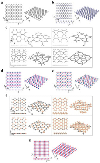
Figure 1. The graphene family: (a) graphene (gray atom represents C), (b) CX (X = H, F, Cl; gray and blue atoms represent C and X, respectively), (c) graphyne (α-graphyne, β-graphyne, γ-graphyne and 6,6,12-graphyne from left to right, top to bottom; gray atom represents C), (d) h-BN (red and blue atoms represent B and N, respectively), (e) BCN (reproduced from Ref. [71]; red, gray and blue atoms represent B, C and N, respectively), (f) SixC1−x(x = 2/10, 5/6, 2/6, 14/18 from left to right, top to bottom; gray and yellow atoms represent C and Si, respectively) (reproduced from Ref. [72]), (g) TiC (reproduced from Ref. [73]; red and blue atoms represent C and Ti, respectively).
Xenes are monoelement 2D materials organized into distorted hexagonal or trigonal lattices. The 2D Xenes can be made up of group IIIA, IVA, and VA elements, termed borophene, silicene, germanene, stanene, phosphorene, and antimonene when X = B, Si, Ge, Sn, P, and Sb, respectively (Figure 2a–c). Unlike the ideally flat structure of graphene, 2D Xenes prefer alternating out-of-plane atomic arrangements, resulting in an anisotropic lattice structure. Due to abundant components and unique structures, 2D Xenes exhibit excellent physical, chemical, and mechanical properties, enabling them to be promising agents for biosensors, bioimaging, therapeutic delivery, and theranostics [74].
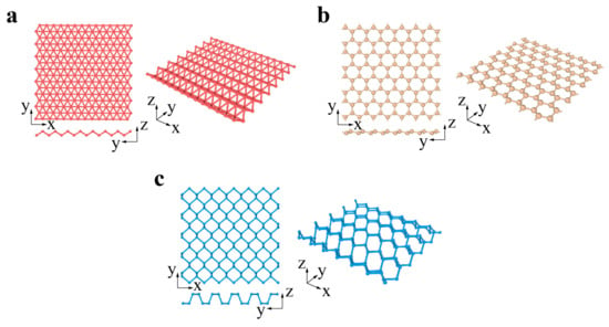
Xenes: (
) borophene, (
) silicene, germanene, stanene and antimonene, (
) phosphorene.
Chalcogenides are a type of emerging 2D material represented by the transitional metal dichalcogenide (TMDC) MX2. For MX2, the layer of transitional metal atom M (Mo, W, Nb, Ta) is sandwiched by two layers of chalcogen atoms X (S, Se, Te). MX2 usually has two typical phases: 2H and 1T phases [75,76,77][75][76][77]. The 2H phases have been widely studied to date. The MX2 (M = Mo, W, Nb, Ta; X = S, Se, Te) in Figure 3a prefers to be the 2H phase in equilibrium, while the MX2 (M = Zr, Hf; X = S, Se) in Figure 3b prefers to be the 1T phase [78,79][78][79]. The transformation from 2H to 1T phases can occur under specific conditions [75,76,77][75][76][77]. GaS, GaSe, and InSe are chalcogenides with a double layer of metal intercalated between two layers of chalcogen, forming an X-M-M-X vertical structure (Figure 3c) [80]. Bi2Te3, Bi2Se3, and Sb2Te3 belong to a specific branch of chalcogenides and are called topological insulators. There exists a van der Waals interaction between the stoichiometric monolayers, e.g., quintuple layers (QLs). A Bi2Se3 QL comprises five atomic layers stacked in the sequence of Se (1)-Bi-Se (2)-Bi-Se (1) along the c-axis (Figure 3d) [81].
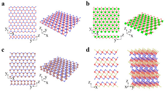
Figure 3. Chalcogenides: (a) 2H-MX2 (M = Mo, W, Nb, Ta; X = S, Se, Te; red and blue atoms represent M and X, respectively), (b) 1T-MX2 (M = Zr, Hf; X = S, Se; green and red atoms represent M and X, respectively), (c) GaS, GaSe and InSe (brown and blue atoms represent Ga or In and S or Se, respectively), (d) Bi2Se3, Bi2Te3 and Sb2Te3 (red atoms represents Bi or Sb, while blue and yellow atoms represent Se or Te in different layers, respectively).
The common types of 2D oxides include lead, phosphorus, and transition metal oxides (Figure 4a–d) [82,83][82][83]. 2D oxides usually appear as single planar structures and multilayer and superlattice structures (Figure 4a–d). Layered 2D oxides have strong lateral chemical bonding in planes but exhibit weak van der Waals interactions between layers, while nonlayered 2D oxides (with superlattice structures) have atomic bonding in three dimensions [84]. Many 2D oxides are functional materials with great potential in catalysis, energy storage, and electronics, since they have a highly chemically active interface [84].
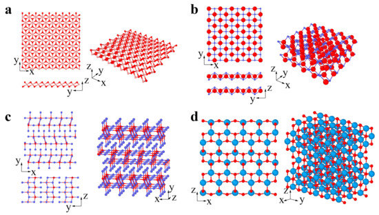
Figure 4. 2D oxides: (a) MnO2 (pink and red atoms represent Mn and O, respectively), (b) PbO (blue and red atoms represent Pb and O, respectively), (c) MoO3 (red and blue atoms represent Mo and O, respectively), (d) TiO2 (azure and red atoms represent Ti and O, respectively).
References
- Novoselov, K.S.; Geim, A.K.; Morozov, S.V.; Jiang, D.; Zhang, Y.; Dubonos, S.V.; Grigorieva, I.V.; Firsov, A.A. Electric field effect in atomically thin carbon films. Science 2004, 306, 666–669.
- Akinwande, D.; Brennan, C.J.; Bunch, J.S.; Egberts, P.; Felts, J.R.; Gao, H.; Huang, R.; Kim, J.-S.; Li, T.; Li, Y.; et al. A review on mechanics and mechanical properties of 2D materials—Graphene and beyond. Extreme Mech. Lett. 2017, 13, 42–77.
- Butler, S.Z.; Hollen, S.M.; Cao, L.; Cui, Y.; Gupta, J.A.; Gutiérrez, H.R.; Heinz, T.F.; Hong, S.S.; Huang, J.; Ismach, A.F.; et al. Progress, challenges, and opportunities in two-dimensional materials beyond graphene. ACS Nano 2013, 7, 2898–2926.
- Wang, Q.H.; Kalantar-Zadeh, K.; Kis, A.; Coleman, J.N.; Strano, M.S. Electronics and optoelectronics of two-dimensional transition metal dichalcogenides. Nat. Nanotechnol. 2012, 7, 699–712.
- Sun, P.; Wang, K.; Zhu, H. Recent developments in graphene-based membranes: Structure, mass-transport mechanism and potential applications. Adv. Mater. 2016, 28, 2287–2310.
- Mas-Balleste, R.; Gomez-Navarro, C.; Gomez-Herrero, J.; Zamora, F. 2D materials: To graphene and beyond. Nanoscale 2011, 3, 20–30.
- Wei, Y.; Yang, R. Nanomechanics of graphene. Natl. Sci. Rev. 2019, 6, 324–348.
- Lee, C.; Wei, X.; Kysar, J.W.; Hone, J. Measurement of the elastic properties and intrinsic strength of monolayer graphene. Science 2008, 321, 385–388.
- Bolotin, K.I.; Sikes, K.J.; Jiang, Z.; Klima, M.; Fudenberg, G.; Hone, J.; Kim, P.; Stormer, H.L. Ultrahigh electron mobility in suspended graphene. Solid State Commun. 2008, 146, 351–355.
- Balandin, A.A.; Ghosh, S.; Bao, W.; Calizo, I.; Teweldebrhan, D.; Miao, F.; Lau, C.N. Superior thermal conductivity of single-layer graphene. Nano Lett. 2008, 8, 902–907.
- Nair, R.R.; Blake, P.; Grigorenko, A.N.; Novoselov, K.S.; Booth, T.J.; Stauber, T.; Peres, N.M.; Geim, A.K. Fine structure constant defines visual transparency of graphene. Science 2008, 320, 1308.
- Wang, F.; Zhang, Y.; Tian, C.; Girit, C.; Zettl, A.; Crommie, M.; Shen, Y.R. Gate-variable optical transitions in graphene. Science 2008, 320, 206–209.
- Lin, Y.M.; Jenkins, K.A.; Valdes-Garcia, A.; Small, J.P.; Farmer, D.B.; Avouris, P. Operation of graphene transistors at gigahertz frequencies. Nano Lett. 2009, 9, 422–426.
- Wu, Y.; Lin, Y.M.; Bol, A.A.; Jenkins, K.A.; Xia, F.; Farmer, D.B.; Zhu, Y.; Avouris, P. High-frequency, scaled graphene transistors on diamond-like carbon. Nature 2011, 472, 74–78.
- Lin, Y.M.; Dimitrakopoulos, C.; Jenkins, K.A.; Farmer, D.B.; Chiu, H.Y.; Grill, A.; Avouris, P. 100-GHz transistors from wafer-scale epitaxial graphene. Science 2010, 327, 662.
- Kim, K.S.; Zhao, Y.; Jang, H.; Lee, S.Y.; Kim, J.M.; Kim, K.S.; Ahn, J.H.; Kim, P.; Choi, J.Y.; Hong, B.H. Large-scale pattern growth of graphene films for stretchable transparent electrodes. Nature 2009, 457, 706–710.
- Jang, H.; Park, Y.J.; Chen, X.; Das, T.; Kim, M.S.; Ahn, J.H. Graphene-based flexible and stretchable electronics. Adv. Mater. 2016, 28, 4184–4202.
- Furchi, M.; Urich, A.; Pospischil, A.; Lilley, G.; Unterrainer, K.; Detz, H.; Klang, P.; Andrews, A.M.; Schrenk, W.; Strasser, G.; et al. Microcavity-integrated graphene photodetector. Nano Lett. 2012, 12, 2773–2777.
- Xia, F.; Mueller, T.; Lin, Y.M.; Valdes-Garcia, A.; Avouris, P. Ultrafast graphene photodetector. Nat. Nanotechnol. 2009, 4, 839–843.
- Gan, X.; Shiue, R.-J.; Gao, Y.; Meric, I.; Heinz, T.F.; Shepard, K.; Hone, J.; Assefa, S.; Englund, D. Chip-integrated ultrafast graphene photodetector with high responsivity. Nat. Photonics 2013, 7, 883–887.
- Mueller, T.; Xia, F.; Avouris, P. Graphene photodetectors for high-speed optical communications. Nat. Photonics 2010, 4, 297–301.
- Stankovich, S.; Dikin, D.A.; Dommett, G.H.; Kohlhaas, K.M.; Zimney, E.J.; Stach, E.A.; Piner, R.D.; Nguyen, S.T.; Ruoff, R.S. Graphene-based composite materials. Nature 2006, 442, 282–286.
- El-Kady, M.F.; Strong, V.; Dubin, S.; Kaner, R.B. Laser scribing of high-performance and flexible graphene-based electrochemical capacitors. Science 2012, 335, 1326–1330.
- Reddy, A.L.; Srivastava, A.; Gowda, S.R.; Gullapalli, H.; Dubey, M.; Ajayan, P.M. Synthesis of nitrogen-doped graphene films for lithium battery application. ACS Nano 2010, 4, 6337–6342.
- Kim, H.; Park, K.Y.; Hong, J.; Kang, K. All-graphene-battery: Bridging the gap between supercapacitors and lithium ion batteries. Sci. Rep. 2014, 4, 5278.
- Yoon, H.J.; Jun, D.H.; Yang, J.H.; Zhou, Z.; Yang, S.S.; Cheng, M.M.-C. Carbon dioxide gas sensor using a graphene sheet. Sens. Actuators B 2011, 157, 310–313.
- Fowler, J.D.; Allen, M.J.; Tung, V.C.; Yang, Y.; Kaner, R.B.; Weiller, B.H. Practical chemical sensors from chemically derived graphene. ACS Nano 2009, 3, 301–306.
- Robinson, J.T.; Perkins, F.K.; Snow, E.S.; Wei, Z.; Sheehan, P.E. Reduced graphene oxide molecular sensors. Nano Lett. 2008, 8, 3137–3140.
- Schneider, G.F.; Kowalczyk, S.W.; Calado, V.E.; Pandraud, G.; Zandbergen, H.W.; Vandersypen, L.M.; Dekker, C. DNA translocation through graphene nanopores. Nano Lett. 2010, 10, 3163–3167.
- Heerema, S.J.; Dekker, C. Graphene nanodevices for DNA sequencing. Nat. Nanotechnol. 2016, 11, 127–136.
- Traversi, F.; Raillon, C.; Benameur, S.M.; Liu, K.; Khlybov, S.; Tosun, M.; Krasnozhon, D.; Kis, A.; Radenovic, A. Detecting the translocation of DNA through a nanopore using graphene nanoribbons. Nat. Nanotechnol. 2013, 8, 939–945.
- Liu, J.; Cui, L.; Losic, D. Graphene and graphene oxide as new nanocarriers for drug delivery applications. Acta Biomater. 2013, 9, 9243–9257.
- Yang, K.; Zhang, S.; Zhang, G.; Sun, X.; Lee, S.T.; Liu, Z. Graphene in mice: Ultrahigh in vivo tumor uptake and efficient photothermal therapy. Nano Lett. 2010, 10, 3318–3323.
- Sun, X.; Liu, Z.; Welsher, K.; Robinson, J.T.; Goodwin, A.; Zaric, S.; Dai, H. Nano-graphene oxide for cellular imaging and drug delivery. Nano Res. 2008, 1, 203–212.
- Mounet, N.; Gibertini, M.; Schwaller, P.; Campi, D.; Merkys, A.; Marrazzo, A.; Sohier, T.; Castelli, I.E.; Cepellotti, A.; Pizzi, G.; et al. Two-dimensional materials from high-throughput computational exfoliation of experimentally known compounds. Nat. Nanotechnol. 2018, 13, 246–252.
- Joensen, P.; Frindt, R.F.; Morrison, S.R. Single-layer MoS2. Mater. Res. Bull. 1986, 21, 457–461.
- Paffett, M.T.; Simonson, R.J.; Papin, P.; Paine, R.T. Borazine adsorption and decomposition at Pt(111) and Ru(001) surfaces. Surf. Sci. 1990, 232, 286–296.
- Nagashima, A.; Tejima, N.; Gamou, Y.; Kawai, T.; Oshima, C. Electronic dispersion relations of monolayer hexagonal boron nitride formed on the Ni(111) surface. Phys. Rev. B 1995, 51, 4606–4613.
- Liu, H.; Neal, A.T.; Zhu, Z.; Luo, Z.; Xu, X.; Tomanek, D.; Ye, P.D. Phosphorene: An unexplored 2D semiconductor with a high hole mobility. ACS Nano 2014, 8, 4033–4041.
- Feng, B.; Zhang, J.; Zhong, Q.; Li, W.; Li, S.; Li, H.; Cheng, P.; Meng, S.; Chen, L.; Wu, K. Experimental realization of two-dimensional boron sheets. Nat. Chem. 2016, 8, 564–569.
- Mannix, A.J.; Zhou, X.-F.; Kiraly, B.; Wood, J.D.; Alducin, D.; Myers, B.D.; Liu, X.; Fisher, B.L.; Santiago, U.; Guest, J.R.; et al. Synthesis of borophenes: Anisotropic, two-dimensional boron polymorphs. Science 2015, 350, 1513–1516.
- Vogt, P.; De Padova, P.; Quaresima, C.; Avila, J.; Frantzeskakis, E.; Asensio, M.C.; Resta, A.; Ealet, B.; Le Lay, G. Silicene: Compelling experimental evidence for graphenelike two-dimensional silicon. Phys. Rev. Lett. 2012, 108, 155501.
- Feng, B.; Ding, Z.; Meng, S.; Yao, Y.; He, X.; Cheng, P.; Chen, L.; Wu, K. Evidence of silicene in honeycomb structures of silicon on Ag(111). Nano Lett. 2012, 12, 3507–3511.
- Dávila, M.E.; Xian, L.; Cahangirov, S.; Rubio, A.; Le Lay, G. Germanene: A novel two-dimensional germanium allotrope akin to graphene and silicene. New J. Phys. 2014, 16, 095002.
- Zhu, F.-F.; Chen, W.-J.; Xu, Y.; Gao, C.-L.; Guan, D.-D.; Liu, C.-H.; Qian, D.; Zhang, S.-C.; Jia, J.-F. Epitaxial growth of two-dimensional stanene. Nat. Mater. 2015, 14, 1020.
- Ji, J.; Song, X.; Liu, J.; Yan, Z.; Huo, C.; Zhang, S.; Su, M.; Liao, L.; Wang, W.; Ni, Z.; et al. Two-dimensional antimonene single crystals grown by van der Waals epitaxy. Nat. Commun. 2016, 7, 13352.
- Nagao, T.; Sadowski, J.T.; Saito, M.; Yaginuma, S.; Fujikawa, Y.; Kogure, T.; Ohno, T.; Hasegawa, Y.; Hasegawa, S.; Sakurai, T. Nanofilm allotrope and phase transformation of ultrathin Bi film on Si(111)-7x7. Phys. Rev. Lett. 2004, 93, 105501.
- Reis, F.; Li, G.; Dudy, L.; Bauernfeind, M.; Glass, S.; Hanke, W.; Thomale, R.; Schafer, J.; Claessen, R. Bismuthene on a SiC substrate: A candidate for a high-temperature quantum spin Hall material. Science 2017, 357, 287–290.
- Zhu, Z.; Cai, X.; Yi, S.; Chen, J.; Dai, Y.; Niu, C.; Guo, Z.; Xie, M.; Liu, F.; Cho, J.H.; et al. Multivalency-driven formation of Te-based monolayer materials: A combined first-principles and experimental study. Phys. Rev. Lett. 2017, 119, 106101.
- Jain, A.; McGaughey, A.J. Strongly anisotropic in-plane thermal transport in single-layer black phosphorene. Sci. Rep. 2015, 5, 8501.
- Watanabe, K.; Taniguchi, T.; Kanda, H. Direct-bandgap properties and evidence for ultraviolet lasing of hexagonal boron nitride single crystal. Nat. Mater. 2004, 3, 404–409.
- Radisavljevic, B.; Radenovic, A.; Brivio, J.; Giacometti, V.; Kis, A. Single-layer MoS2 transistors. Nat. Nanotechnol. 2011, 6, 147–150.
- Lopez-Sanchez, O.; Lembke, D.; Kayci, M.; Radenovic, A.; Kis, A. Ultrasensitive photodetectors based on monolayer MoS2. Nat. Nanotechnol. 2013, 8, 497–501.
- Yin, Z.; Li, H.; Li, H.; Jiang, L.; Shi, Y.; Sun, Y.; Lu, G.; Zhang, Q.; Chen, X.; Zhang, H. Single-layer MoS2 phototransistors. ACS Nano 2012, 6, 74–80.
- Fang, H.; Chuang, S.; Chang, T.C.; Takei, K.; Takahashi, T.; Javey, A. High-performance single layered WSe2 p-FETs with chemically doped contacts. Nano Lett. 2012, 12, 3788–3792.
- Mannix, A.J.; Zhang, Z.; Guisinger, N.P.; Yakobson, B.I.; Hersam, M.C. Borophene as a prototype for synthetic 2D materials development. Nat. Nanotechnol. 2018, 13, 444–450.
- Adamska, L.; Sadasivam, S.; Foley, J.J.; Darancet, P.; Sharifzadeh, S. First-principles investigation of borophene as a monolayer transparent conductor. J. Phys. Chem. C 2018, 122, 4037–4045.
- Ji, Q.; Li, C.; Wang, J.; Niu, J.; Gong, Y.; Zhang, Z.; Fang, Q.; Zhang, Y.; Shi, J.; Liao, L.; et al. Metallic vanadium disulfide nanosheets as a platform material for multifunctional electrode applications. Nano Lett. 2017, 17, 4908–4916.
- Wang, J.; Xu, Y.; Zhang, S.-C. Two-dimensional time-reversal-invariant topological superconductivity in a doped quantum spin-Hall insulator. Phys. Rev. B 2014, 90, 054503.
- Albrecht, T.R.; Mizes, H.A.; Nogami, J.; Park, S.-I.; Quate, C.F. Observation of tilt boundaries in graphite by scanning tunneling microscopy and associated multiple tip effects. Appl. Phys. Lett. 1988, 52, 362–364.
- Kim, K.; Lee, Z.; Regan, W.; Kisielowski, C.; Crommie, M.F.; Zettl, A. Grain boundary mapping in polycrystalline graphene. ACS Nano 2011, 5, 2142–2146.
- Haugan, T.; Barnes, P.N.; Wheeler, R.; Meisenkothen, F.; Sumption, M. Addition of nanoparticle dispersions to enhance flux pinning of the YBa2Cu3O7−x superconductor. Nature 2004, 430, 867–870.
- Balog, R.; Jorgensen, B.; Nilsson, L.; Andersen, M.; Rienks, E.; Bianchi, M.; Fanetti, M.; Laegsgaard, E.; Baraldi, A.; Lizzit, S.; et al. Bandgap opening in graphene induced by patterned hydrogen adsorption. Nat. Mater. 2010, 9, 315–319.
- Bagri, A.; Mattevi, C.; Acik, M.; Chabal, Y.J.; Chhowalla, M.; Shenoy, V.B. Structural evolution during the reduction of chemically derived graphene oxide. Nat. Chem. 2010, 2, 581–587.
- Ito, Y.; Tanabe, Y.; Qiu, H.J.; Sugawara, K.; Heguri, S.; Tu, N.H.; Huynh, K.K.; Fujita, T.; Takahashi, T.; Tanigaki, K.; et al. High-quality three-dimensional nanoporous graphene. Angew. Chem. Int. Ed. Engl. 2014, 53, 4822–4826.
- Lahiri, J.; Lin, Y.; Bozkurt, P.; Oleynik, I.I.; Batzill, M. An extended defect in graphene as a metallic wire. Nat. Nanotechnol. 2010, 5, 326–329.
- Zhang, Y.Y.; Pei, Q.X.; Wang, C.M. Mechanical properties of graphynes under tension: A molecular dynamics study. Appl. Phys. Lett. 2012, 101, 081909.
- Malko, D.; Neiss, C.; Vines, F.; Gorling, A. Competition for graphene: Graphynes with direction-dependent Dirac cones. Phys. Rev. Lett. 2012, 108, 086804.
- Li, G.; Li, Y.; Liu, H.; Guo, Y.; Li, Y.; Zhu, D. Architecture of graphdiyne nanoscale films. Chem. Commun. 2010, 46, 3256–3258.
- Li, Y.; Xu, L.; Liu, H.; Li, Y. Graphdiyne and graphyne: From theoretical predictions to practical construction. Chem. Soc. Rev. 2014, 43, 2572–2586.
- Beniwal, S.; Hooper, J.; Miller, D.P.; Costa, P.S.; Chen, G.; Liu, S.Y.; Dowben, P.A.; Sykes, E.C.; Zurek, E.; Enders, A. Graphene-like Boron-Carbon-Nitrogen monolayers. ACS Nano 2017, 11, 2486–2493.
- Shi, Z.; Zhang, Z.; Kutana, A.; Yakobson, B.I. Predicting two-dimensional silicon carbide monolayers. ACS Nano 2015, 9, 9802–9809.
- Zhang, Z.; Liu, X.; Yakobson, B.I.; Guo, W. Two-dimensional tetragonal tic monolayer sheet and nanoribbons. J. Am. Chem. Soc. 2012, 134, 19326–19329.
- Wang, T.; Wang, H.; Kou, Z.; Liang, W.; Luo, X.; Verpoort, F.; Zeng, Y.J.; Zhang, H. Xenes as an emerging 2D monoelemental family: Fundamental electrochemistry and energy applications. Adv. Funct. Mater. 2020, 30, 2002885.
- Kappera, R.; Voiry, D.; Yalcin, S.E.; Branch, B.; Gupta, G.; Mohite, A.D.; Chhowalla, M. Phase-engineered low-resistance contacts for ultrathin MoS2 transistors. Nat. Mater. 2014, 13, 1128–1134.
- Lin, Y.C.; Dumcenco, D.O.; Huang, Y.S.; Suenaga, K. Atomic mechanism of the semiconducting-to-metallic phase transition in single-layered MoS2. Nat. Nanotechnol. 2014, 9, 391–396.
- Duerloo, K.A.; Li, Y.; Reed, E.J. Structural phase transitions in two-dimensional Mo- and W-dichalcogenide monolayers. Nat. Commun. 2014, 5, 4214.
- Gong, C.; Zhang, H.; Wang, W.; Colombo, L.; Wallace, R.M.; Cho, K. Band alignment of two-dimensional transition metal dichalcogenides: Application in tunnel field effect transistors. Appl. Phys. Lett. 2013, 103, 053513.
- Zhen, Y.-X.; Yang, M.; Zhang, H.; Fu, G.-S.; Wang, J.-L.; Wang, S.-F.; Wang, R.-N. Ultrahigh power factors in P-type 1T-ZrX2 (X = S, Se) single layers. Sci. Bull. 2017, 62, 1530–1537.
- Yagmurcukardes, M.; Senger, R.T.; Peeters, F.M.; Sahin, H. Mechanical properties of monolayer GaS and GaSe crystals. Phys. Rev. B 2016, 94, 245407.
- Zhang, H.; Liu, C.-X.; Qi, X.-L.; Dai, X.; Fang, Z.; Zhang, S.-C. Topological insulators in Bi2Se3, Bi2Te3 and Sb2Te3 with a single Dirac cone on the surface. Nat. Phys. 2009, 5, 438–442.
- Azadmanjiri, J.; Srivastava, V.K.; Kumar, P.; Wang, J.; Yu, A. Graphene-supported 2D transition metal oxide heterostructures. J. Mater. Chem. A 2018, 6, 13509–13537.
- Kumar, P.; Liu, J.; Ranjan, P.; Hu, Y.; Yamijala, S.S.; Pati, S.K.; Irudayaraj, J.; Cheng, G.J. Alpha lead oxide (α-PbO): A new 2D material with visible light sensitivity. Small 2018, 14, 1703346.
- Haque, F.; Daeneke, T.; Kalantar-Zadeh, K.; Ou, J.Z. Two-dimensional transition metal oxide and chalcogenide-based photocatalysts. Nano-Micro Lett. 2018, 10, 23.