Contact scaling is a major challenge in nano complementary metal–oxide–semiconductor (CMOS) technology, as the surface roughness, contact size, film thicknesses, and undoped substrate become more problematic as the technology shrinks to the nanometer range. These factors increase the contact resistance and the nonlinearity of the current–voltage characteristics, which could limit the benefits of the further downsizing of CMOS devices.
- metal/semiconductor contact
- Schottky contact
- ohmic contact
- 2D material/metal contacts
- contact scaling
1. Introduction
2. Schottky Junction
2.1. Schottky Equation
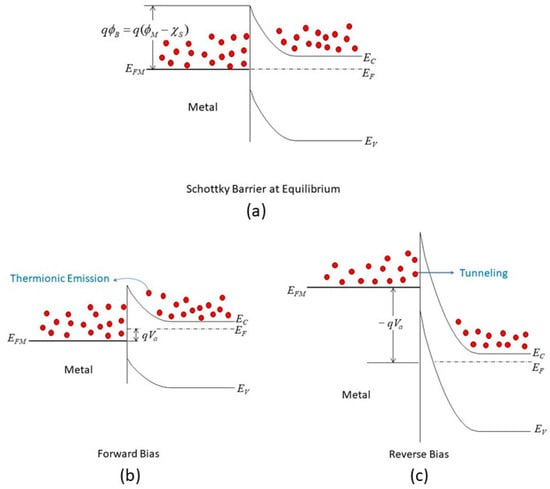
The key component of the Schottky equation is the thermal emission law, as proposed by Richardson [34][18], which was based on experimental results related to the current density generated from a heated metal wire. The temperature and current dependencies are as follows: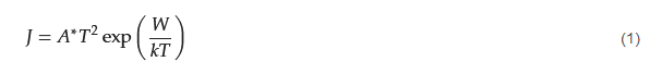 where W is the workfunction of the metal, kT is the thermal voltage, and A* is the effective Richardson constant. Schottky later modified the expression to include the effect of an electric field, and its final form is now usually expressed in terms of an applied voltage, V, as follows [32,33][16][17]:
 where q is the electron charge, and ΦSB is the Schottky barrier.
In the original proposal by Schottky and Mott [32[16][17],33], the Schottky barrier is as follows”
where q is the electron charge, and ΦSB is the Schottky barrier.
In the original proposal by Schottky and Mott [32[16][17],33], the Schottky barrier is as follows”


2.2. Current Conduction in an MIS Diode
The Schottky equation can be used to model the current conduction of an MIS diode. However, this equation is based on some assumptions that are often overlooked. It is also suggested that, in some early metal/semiconductor contacts, there may exist some native thin oxide on the semiconductor’s surface. Fowler suggested that there was a layer of “bad semiconductor” between a metal and a good semiconductor [31][15]. Although these proposals were later refuted, it did point to the importance of the interface’s quality in the contact behavior. A similar situation arose in the recent study of 2D material contacts and 2D material/Si contacts, in which a thin tunneling layer may be present between the metal and the 2D material. In this case, the Schottky equation can still be used to approximate the tunneling current in the forward region but with a modified effective Richardson constant that accounts for the tunneling barrier [42][26]. The modified Schottky equation is as follows: where is the χ mean barrier height value between the insulator and the semiconductor and δ is the tunneling oxide thickness. It can define a new effective Richardson constant as follows:
 Note that the current conduction is, in fact, dominated by the direct tunneling of the carriers over the thin insulating layer. The approximation of the Schottky equation involves modifying the Richardson coefficient with a transmission coefficient, which depends on the barrier height between the silicon and the insulator and the insulator thickness. These two factors are the key parameters that govern the conduction current. In addition, some effects, such as the minority carrier injection, image force, and quantum mechanism reflection, are also neglected. This approximation is only valid for a forward current with V > 3kT/q, because the metal/insulator barrier differs from the silicon/insulator barrier. Some authors have ignored these assumptions and treated the MIS diode as a regular Schottky diode.
Instead of treating the n factor as an “ideality factor” in (8), it was proposed that the nonunity n factor could be calculated from the surface potential of the barrier [42][26]. Defining n as a change in the surface potential, ΔVs, with respect to the applied voltage (i.e., 𝑛=−𝑉/Δ𝑉𝑠), and further taking the interface states into consideration, the electrostatic calculation leads to the following:
Note that the current conduction is, in fact, dominated by the direct tunneling of the carriers over the thin insulating layer. The approximation of the Schottky equation involves modifying the Richardson coefficient with a transmission coefficient, which depends on the barrier height between the silicon and the insulator and the insulator thickness. These two factors are the key parameters that govern the conduction current. In addition, some effects, such as the minority carrier injection, image force, and quantum mechanism reflection, are also neglected. This approximation is only valid for a forward current with V > 3kT/q, because the metal/insulator barrier differs from the silicon/insulator barrier. Some authors have ignored these assumptions and treated the MIS diode as a regular Schottky diode.
Instead of treating the n factor as an “ideality factor” in (8), it was proposed that the nonunity n factor could be calculated from the surface potential of the barrier [42][26]. Defining n as a change in the surface potential, ΔVs, with respect to the applied voltage (i.e., 𝑛=−𝑉/Δ𝑉𝑠), and further taking the interface states into consideration, the electrostatic calculation leads to the following:
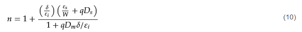 where εi and εs are the permittivities of the insulator and semiconductor, respectively; W is the depletion layer in the semiconductor surface; and Ds and Dm are the surface state densities in the equilibrium with the semiconductor and metal, respectively. If the surface state is negligible, (10) reduces to the following:
 Thus, large n values, in some cases, are not mysterious; it is only because the electrostatic thickness of the insulating layer, 𝛿/𝜀𝑖, is much larger than the electrostatic thickness of the depletion layer width, 𝑊/𝜀𝑠. If neglecting the surface states on the metal side, which is the case for most MIS diodes, Equation (10) reduces to the following:
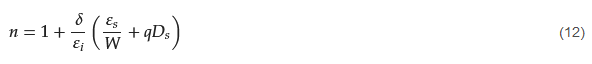 In this expression, n is a parameter that describes how effectively the barrier surface potential varies with the applied voltage. It has nothing to do with the generation and recombination of carriers or the validity of the Schottky current model. Therefore, it is not an indicator of the ideality of the junction.
In fact, the validity of (8) for the MIS diode is limited. The conduction current should be more precisely modeled by the direct tunneling current (see Equation (13)) if the insulator layer and barrier height are in the direct tunneling range [43,44][27][28].
In this expression, n is a parameter that describes how effectively the barrier surface potential varies with the applied voltage. It has nothing to do with the generation and recombination of carriers or the validity of the Schottky current model. Therefore, it is not an indicator of the ideality of the junction.
In fact, the validity of (8) for the MIS diode is limited. The conduction current should be more precisely modeled by the direct tunneling current (see Equation (13)) if the insulator layer and barrier height are in the direct tunneling range [43,44][27][28].
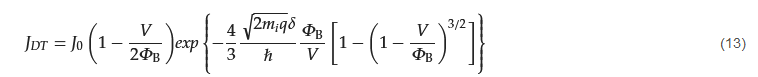 where mi is the electron mass in the oxide; ℏ is the reduced Planck’s constant; and ΦB is the barrier height (in electron volts) between the emitting electrode and the oxide.
For the case of thicker insulators or with a smaller voltage applied, tunneling over the triangular edge (see Figure 32c) is also possible. In this situation, the current conduction is better described with the Fowler–Nordheim (FN) equation, as shown below [45][29]:
where mi is the electron mass in the oxide; ℏ is the reduced Planck’s constant; and ΦB is the barrier height (in electron volts) between the emitting electrode and the oxide.
For the case of thicker insulators or with a smaller voltage applied, tunneling over the triangular edge (see Figure 32c) is also possible. In this situation, the current conduction is better described with the Fowler–Nordheim (FN) equation, as shown below [45][29]:
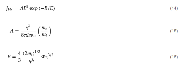 where me is the electron mass in the free space.
The FN formula has been widely used to explain the conduction behavior of various thin dielectric films [45][29]. However, in contact studies including the so-called MIS Schottky diode, the current–voltage characteristics were often fitted with the modified Schottky Equation (8) or even the simple Schottky equation in (7) instead of the FN relationship. It has to be pointed out that the barrier height extracted from these fitting should be inaccurate, and the ideality factor does not carry any technical implications. The effective Richardson coefficient is also inappropriate in these cases. The current–voltage characteristics are better described with the FN equation.
where me is the electron mass in the free space.
The FN formula has been widely used to explain the conduction behavior of various thin dielectric films [45][29]. However, in contact studies including the so-called MIS Schottky diode, the current–voltage characteristics were often fitted with the modified Schottky Equation (8) or even the simple Schottky equation in (7) instead of the FN relationship. It has to be pointed out that the barrier height extracted from these fitting should be inaccurate, and the ideality factor does not carry any technical implications. The effective Richardson coefficient is also inappropriate in these cases. The current–voltage characteristics are better described with the FN equation.
3. Ohmic Contact in the Nanoscale
Ohmic contact refers to a metal–semiconductor contact with low and constant resistance regardless of the applied voltage polarity. A low contact resistance and nonrectifying contact enable signals to transmit into and out of a semiconductor device, such as transistors, LEDs, and solar cells, with minimum distortion. Figure 53a,b illustrate the idea for achieving an n-type ohmic contact. A small contact barrier can be obtained by choosing a small metal workfunction. Under forward bias, the electron can be emitted through the barrier via thermionic emission or Schottky emission. With reverse bias (see Figure 53b), the barrier height is increased, but a large reverse current is still possible if the barrier width is narrow enough so that direct tunneling is possible. The ohmic contact has not been considered a server-challenging issue since the start of silicon technology. The key factor governed by the contact resistance can be readily solved with the well-developed metallization and junction doping technique. The narrow barrier is achieved by heavily doping the contact region of the semiconductor. In addition, the junction dimensions, including the cross-sectional area, junction depth, and metal thickness, are quite large compared to the devices themselves. Figure 53c illustrates the ideal ohmic contact’s characteristics, practical ohmic contact, and the scaling effect of the contact. As mentioned, to reduce the signal loss, the contact resistance should be as small as possible. The current–voltage (I–V) relationship in the prescribed voltage range should be linear so that it does not cause signal distribution and harmonics. However, as illustrated in Figure 53a,b, barriers exist in the metal/semiconductor contact; the I–V characteristics are either governed by thermionic emission or tunneling, which are nonlinear. In addition, because the forward and reverse conductions are controlled by different mechanisms, the I–V characteristics are asymmetric. The degrees of nonlinearity and asymmetry may not cause significant issues when the signal levels are high.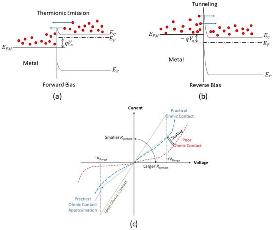
- (1)
-
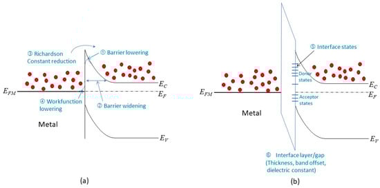
Barrier lowering: The barrier height at the interface can be reduced by various factors, such as image force effects, metal workfunction variation, and surface roughness. These factors may be negligible in a large junction, but they can have significant impacts in a scaled junction. They can increase the forward current by lowering the potential barrier.
- (2)
-
Barrier widening: The use of heavily doped contacts may not be possible in a scaled junction. This can result in a wider tunneling barrier, which reduces the conduction current under reverse bias.
- (3)
-
Richardson constant reduction: Thinner metal films are used in a scaled junction, which can lead to a smaller value of the Richardson constant. This can decrease the forward current by reducing the thermionic emission.
- (4)
-
Metal workfunction lowering: experimental results suggest that thinner metal films have lower workfunctions [46][30], which can also reduce the barrier height at the interface.
- (5)
-
Interface states: The presence of interface states can cause Fermi-level pinning, which affects the barrier height and the band bending. This effect is more pronounced in thinner films and in unpassivated surfaces.
- (6)
-
Interface layer: To mitigate the Fermi-level pinning effect or to enable different circuit design options, such as using 2D materials as interlayer conductors (see Section 4.5), an interface layer may be used for passivation. This can affect the reverse currents by changing the tunneling characteristics. The thickness, band offset, and dielectric constant of the interface layer are important parameters for this effect.
3.1. Effects of Junction Doping
The unavailability of a heavily doped contact results in a wider barrier. As shown in Figure 75a, this reduces the tunneling efficiency. Following the method developed by Yu [47][31], it can calculate the contact resistance depending on the dopant concentration. Figure 86 shows the contact resistance as a function of the dopant concentration. For high dopant concentrations (>2.5 × 1019 cm−3), the contact resistance decreases to the range of 10−5 to 10−6 Ω-cm2. The current conduction is mainly due to field emission.
Figure 86. Illustration of doping concentration dependence of contact resistance involving different current conduction mechanisms.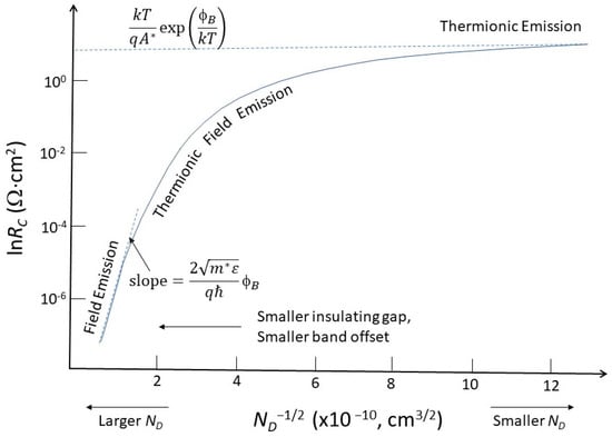
3.2. Effects of Interface Roughness
The Schottky current of a metal/semiconductor can exceed the Schottky–Mott limit. Fundamental calculations show that the metal surface flatness affects the electron cloud near it [48,49][32][33]. It was found that the ratio of electric field fluctuations to the average electric field, denoted by δE/ES, can be estimated by the following [49][33]: where Es denotes the electric field resulting from a smooth surface; 𝛿 E is the increased electric field due to the surface roughness; k is related to the surface wave vector; Δ is the normalized roughness; lcor is the normalized correlation length; r is the roughness exponent, which is a measure of the degree of surface irregularity; and a is a proportional constant. See Figure 97 for the definitions of the parameters.
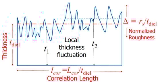 Figure 97. Definitions of the key roughness parameters and an illustration of the local averaged thickness variation for small-sized devices as a function of the applied field [50][34].Figure 97 shows how the roughness parameter, Δ, and the correlation length, lcor, are normalized by the film thickness, tdiel. The normalized roughness Δ (=rs/tdiel) becomes more important for films with similar thicknesses. The correlation length, which measures the local field variation, is also inversely related to the film thickness, i.e., lcor = Lcor/tdiel. This means that thinner films have larger values of Δ and lcor and, therefore, larger electric field fluctuations [50][34].One of the factors that affect the electrical properties of metal–insulator–metal (MIM) structures is the surface roughness of the interfaces. The lower interface (insulator on metal) tends to be rougher than the upper interface (metal on insulator) due to the crystalline nature and the grain size of the metal films, as well as the limitations of the deposition methods, such as evaporation or sputtering. This phenomenon has been known for decades and persists even in MIM structures with larger dimensions and thicker films [51,52,53,54,55,56][35][36][37][38][39][40].The electrical properties of metal/semiconductor contacts strongly depend on the metal film thickness and, also, the method of deposition [46][30]. These effects may be partly related to the surface roughness. Figure 118 shows how the Schottky barrier height and Richardson constant vary with the metal thickness and deposition process. For an evaporated sample with a 100 Å thickness (see Figure 118a), the Cu electrode has a barrier height of approximately 0.58 eV and a Richardson constant close to the theoretical value of 112 A/cm2/K2. Both parameters increase sharply and reach their saturation values of about twice the theoretical value for the Richardson constant and 0.62 eV for the barrier height for films thicker than 200 Å.Figure 118. The metal thickness and deposition process are dependent on the Schottky barrier height and Richardson constant: (a) Cu-Si contacts by evaporation; (b) sputtered Cu-Si contacts prepared by sputtering. Redrawn based on [46][30].
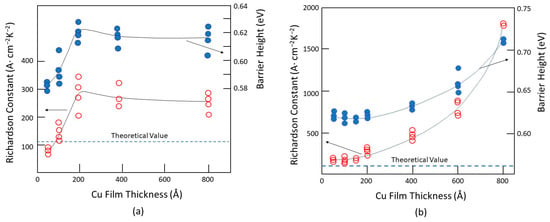
4. Contacts for 2D Materials
Two-dimensional materials, especially transition metal dichalcogenides (TMDs), such as molybdenum disulfide (MoS2) [21[41][42][43],22,23], ditelluride (MoTe2) [24[44][45],25], tungsten diselenide (WSe2) [26[46][47],27], and phosphorene, are considered to be possible replacements for silicon when silicon-based CMOS devices reach their physical limits [15,16,17,18,19,20][48][49][50][51][52][53]. These materials, which have high electron mobility, low optical absorption coefficient, and high electrical and thermal conductivities, could enhance the device and circuit performance in many aspects. However, there are still unresolved challenges related to mass production, complex device design, and circuit integration [15,16][48][49].Most of the reported 2D-material-based devices are currently much bigger than CMOS technology, even though 2D materials are often linked to nanodevices and nanotechnology in the literature. Achieving a good ohmic contact at the submicrometer scale is still a difficult problem. Because the films are only a few monolayers thick and the dopant concentration is far less than that of conventional semiconductors, the contact resistances of metal/2D materials are much larger than that of conventional semiconductors. Shen et al. reported an ultralow resistance ohmic contact based on semi-metallic bismuth on monolayer TMD materials. The Schottky barrier height was reduced to a zero voltage [59][54]. There is a large body of literature on 2D-material-based Schottky contact devices from over the last decade [60,61,62,63,64,65][55][56][57][58][59][60].Figure 159 shows the main features and challenges of metal/2D material contacts, which are summarized as follows: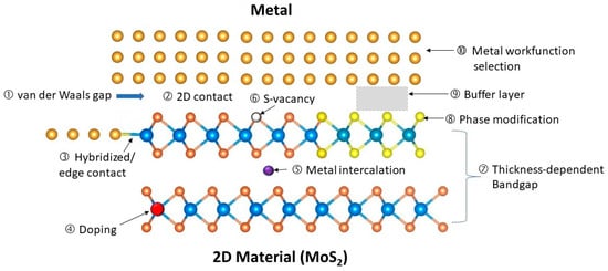 Figure 159.Illustration of the issues and features associated with metal–2D material (MoS2, as an example) contacts.
- (1)
-
van der Waals gap: This is a tunneling barrier between the metal and the 2D material that allows for the tunneling of electrons. Some 2D materials may also form strong bonds with the metal or by overlapping their orbitals.
- (2)
-
2D contact: This is a common method of connecting 2D material from the top, but it has a high resistance per area because the current flows parallel to the 2D plane, not perpendicular to it. A top contact is easier to achieve because it involves depositing metal on the surface of the 2D materials and patterning it with standard photolithography.
- (3)
-
Hybridization and edge contact: This is a better alternative to the 2D contact, as it creates a physical bond and a direct current path along the surface of the 2D material. However, it is challenging to achieve, because it requires the precise alignment and deposition of metal on very thin edges. Some 2D materials may also form strong bonds with the metal or by overlapping their orbitals.
- (4)
-
Doping: 2D materials cannot be doped in the conventional ways, and it is hard to dope heavily.
- (5)
-
Metal intercalation: This is a process of incorporating metal atoms into the gaps of multilayer 2D materials. The dopants contribute to the current’s conduction and can improve the contact’s conductivity.
- (6)
-
Surface defects: These are imperfections, such as sulfur (S) vacancy in MoS2, on the 2D material surface that can trap charges and pin the Fermi level, affecting the contact potential and resistance.
- (7)
-
Layer-dependent bandgap: The bandgap and the contact potential of the 2D material vary with the number of layers. This can be exploited to tune the contact properties by changing the layer thickness in the contact region.
- (8)
-
Phase modification: Some 2D materials can switch among different phases that have distinct electrical properties. For instance, the 2H phase of TMDs is semiconducting, while the 1T and 1T0 phases are metallic. By changing the contact region to a metallic phase, the contact conductivity can be enhanced significantly.
- (9)
-
Buffer layer insertion: inserting a buffer layer between the metal and the 2D material can help reduce the effects of the van der Waals gap and the metal-induced gap states.
- (10)
-
Metal workfunction selection: To achieve good ohmic contact with both n-type and p-type 2D materials, various unconventional metals, such as In, Mg, Ag, Pd, Sc, and Ti, have been explored. However, not much work has addressed the issues of stability, reliability, and potential process contamination. For digital circuit applications, one must consider whether these metals can produce the desired threshold voltages for n-type and p-type transistors.
4.1. Metal van der Waals Contacts and Hybridized Contacts
One of the challenges in fabricating devices based on 2D materials is to ensure a good contact between the 2D lattice and the 3D metal electrodes, without damaging the 2D structure or creating interface defects. To address this issue, some researchers have developed techniques to integrate 3D metal layers with 2D materials using van der Waals (vdWs) forces. These techniques preserve the integrity of the 2D lattice and avoid chemical bonding. For example, Liu et al. [63][58] devised a novel method to transfer atomically smooth metal layers onto 2D semiconductors. The procedure involved patterning and depositing the metal layer on an atomically flat Si substrate, then covering it with a PMMA film to enable its detachment. Afterward, a PDMS stamp was employed to lift the PMMA-coated metal layer and align it precisely on the target surface of the 2D material. On the basis of this method, the Schottky barrier height obtained was close to the Schottky–Mott model and had a large pinning factor of 0.96.
From a fabrication process and device operation point of view, there should be a better approach to achieving covalent bonding between 2D materials and metals. An intimate contact would help to eliminate the interfacial tunneling barrier and enhance the carrier injection efficiency. Side or edge contacts on 2D materials are one way to obtain these kinds of metal/2D material contacts. The edge contacts can be fabricated by using either top-down or bottom-up approaches. In a top-down scheme, an insulating layer, such as Al2O3 or h-BN, is first deposited on the 2D channel. It is then selectively etched to expose the 2D edges. It was reported that edge-contacted graphene FETs can have a contact resistance as low as 100 Ω·mm while maintaining a high charge carrier mobility [66][61]. Some metal/2D material contacts are not thermally stable. The contact characteristics are affected by the interface interaction. McDonnell et al. observed a thin layer of TiO2 when Ti was deposited on MoS2 with a vacuum pressure of 10−6 mbar. This layer was found to have a negligible conduction band offset with MoS2 and resulted in a low contact resistance [70][62]. However, when Ti was deposited in an ultrahigh vacuum of 10−9 mbar, the Ti atoms reacted with MoS2, and a TixSy phase formed, which resulted in a much larger contact resistance. The formation of TiO2 should be due to the residual oxygen or water molecules in the vacuum system or metal. The thin TiO2 layer inhibits the direct chemical reaction of Ti and S. At an ultrahigh vacuum, the oxygen and water residuals are significantly reduced, and the direct reaction of Ti and S is possible. TixSy has poor electrical conductivity. However, Au/MoS2 contacts were also found to be dependent on the deposition pressure. To realize CMOS devices with 2D-material-based transistors, achieving both n-type and p-type devices on a single-type 2D material and with the same metal contacts is essential. It was discovered that the polarity of multilayer MoTe2 encapsulated in h-BN can be varied by applying thermal annealing at different temperatures [72][63].4.2. Junction Doping
High substrate doping has been the key strategy in conventional semiconductor technology to achieve ohmic contacts in CMOS technology. Conventional semiconductors can use different doping techniques, such as ion implantation and plasma immersion ion implantation [1], to increase the doping concentration to a degeneracy level. However, these methods are not compatible with 2D materials that have only a few atomic layers. A more effective doping method for 2D materials is spontaneous charge transfer doping (SCTD) [73,74][64][65]. For p-type doping, the energy difference between the top of the valance band of the 2D material and the lowest unoccupied molecular orbital (LUMO) of the surface doping will cause electron transfer, which leads to hole accumulation and the lifting upward of the valence band in the semiconductor surface region. Similarly, suppose the bottom of the conduction band of the 2D material is below the highest occupied molecular orbital (HOMO) of the surface dopant; electrons will transfer from the HOMO of the surface dopant to the conduction band of the semiconductor and result in the electron doping. A wide range of dopants for various 2D materials are available [73][64].4.3. Bandgap Modification and Band Alignment
Band alignment can be achieved by selecting a metal with a suitable workfunction. Previous studies have shown that the contact potential depends on the type of surface termination [81][66]. For top contacts with a monolayer of MoS2, the Fermi-level pinning is close to the conduction band edge, and n-type Schottky barriers are formed. In this case, Al, In, and Mg may be good candidates for ohmic contacts. The edge contacts, either armchair or zigzag termination of Mo and S atoms, result in a Fermi-level pinning near the valence band, and p-type Schottky barriers are formed. Two-dimensional material has a distinct nature in that the bandgap can be readily tuned by stacking a different number of 2D monolayers. The bandgaps of 2D materials vary with the number of layers and their stacking configurations, which influences the quantum confinement effects. On the basis of the first-principles calculations, Wickramaratne et al. found that the band gap of a single monolayer of hexagonal boron nitride (h-BN) is a direct bandgap semiconductor; the gap becomes indirect for multiple layers [82][67]. The positions of the band edges, with respect to the vacuum level, shift by 0.5 eV for the direct-to-indirect transition. Thickness-dependent bandgap characteristics were also found in other 2D materials.4.4. Phase Modification
Two-dimensional materials can exist in different crystal structures or phases. Different phases have different electronic and optical properties and, thus, different metal contact behaviors as well [84,85][68][69]. For example, 2H-TMDs are semiconducting materials with a trigonal prismatic structure, while 1T and 1T0 phases are metallic materials with an octahedral structure. Using n-butyllithium to induce a phase transition from 2H to 1T’ or 1T0 in a MoS2 nanosheet, Kappera et al. achieved a significant reduction in contact resistance to 0.24 kΩ⋅μm [85][69].
4.5. Fermi-Level Pinning and Buffer Layer
The interface states at two-dimensional material/metal interfaces can affect the performance of two-dimensional devices. These states include metal-induced gap states (MIGS) and defect states, which can induce Fermi-level pinning (FLP) at the interface and hinder the carrier injection efficiency. Fermi-level pinning causes adverse effects in 2D material/metal contacts. It was proposed to be one of the main reasons for the experimental observations of large contact resistance. The origins of the FLP effect at the 2D material/metal interface should be due to several causes. A buffer layer can reduce the effects of metal-induced gap states (MIGS) by creating a matching layer between the 2D material and the metal. This idea was inspired by previous work on high-performance metal–insulator–semiconductor (MIS) diodes [33,42][17][26]. The buffer layer prevents the metal wave function from penetrating the semiconductor material, which lowers the MIGS density. Moreover, if the buffer layer is an insulator, it can balance the charge at the interface and shift the Fermi-level closer to the charge neutrality level, which further decreases the effective Schottky barrier height. One of the most often used buffer materials for 2D material/metal contacts is graphene. Graphene has a semi-metallic nature and a tunable workfunction. By inserting prepatterned single-layer graphene between MoS2 and metal, Chee and co-workers created a sandwich contact structure for MoS2 FETs [93][70]. The graphene layer enhanced the contact between MoS2 and Ag significantly. The Schottky barrier height was reduced to 190 meV due to the charge transfer from Ag to graphene that matched the Fermi level of graphene with a conduction band edge of MoS2. This increased the electron mobility by almost three times. Graphene is not the only metallic 2D material that can act as an interfacial buffer layer to achieve ohmic contacts for 2D-material-based devices.
5. 2D Contact with Silicon
The current 2D-material-based electron devices are still much larger than state-of-the-art CMOS technology. There is a lack of mass production and large-scale integration technology for these devices. Therefore, it is unlikely that 2D-material-based ICs will replace the mainstream silicon technology in the next ten years. However, it is highly possible that some 2D materials will be integrated with Si technology to overcome some of the limitations of CMOS devices and fabrication technology and to enhance the performance of silicon devices. For instance, using 2D materials instead of the expensive indium tin oxide (ITO) films in photonic devices could be a promising option for 2D materials/Si technology integration. Graphene–silicon solar cells have been extensively studied since the discovery of graphene [103,104,105][71][72][73]. However, some fundamental issues of the graphene/silicon interface are still not well understood. Some puzzling issues, such as the wide variations in Schottky barrier height and large fluctuations in the ideality factor (from ~1 to 30), were observed in this simple structure [41,96][25][74]. These wide ranges in parameter values suggest that some additional physical mechanisms in addition to the Schottky emission should be considered. The interface between 2D material and silicon has a unique nature that is not common in the conventional silicon process and is also unknown to the 2D material community [41][25]. Two-dimensional materials, such as graphene, have a much lower surface defect density than most conventional semiconductor materials. However, silicon has many dangling bonds on its surface. The van der Waals contact of the graphene/Si interface would leave a large number of unpassivated silicon dangling bonds.
References
- Iwai, H.; Sze, S.M.; Taur, Y.; Wong, H. MOSFETs. In Guide to State-of-the-Art Electron Devices; Burghartz, J.N., Ed.; Wiley and IEEE: Hoboken, NJ, USA, 2013; pp. 21–36.
- Moore, G.E. Cramming More Components onto Integrated Circuits. Electronics 1965, 38, 114–117.
- Wong, H.; Iwai, H. The road to miniaturization. Phys. World 2005, 18, 40.
- Dennard, R.H.; Gaensslen, F.; Yu, H.-N.; Rideout, L.; Bassous, E.; LeBlanc, A. Design of ion-implanted MOSFET’s with very small physical dimensions. IEEE J. Solid-State Circuits 1974, 9, 256–268.
- Semiconductor Industry Association, 2013 International Technology Roadmap for Semiconductors. Available online: https://www.semiconductors.org/resources/2013-international-technology-roadmap-for-semiconductors-itrs/ (accessed on 30 December 2019).
- Wong, H.; Iwai, H. On the Scaling of Subnanometer EOT Gate Dielectrics for Ultimate nano CMOS Technology. Microelectron. Eng. 2015, 138, 57–76.
- Wong, H. On the CMOS Device Downsizing, More Moore, More than Moore, and More-than-Moore for More Moore. In Proceedings of the 2021 IEEE 32nd International Conference on Microelectronics (MIEL), Nis, Serbia, 12–14 September 2021; pp. 9–15.
- Wong, H.; Kakushima, K. Poole–Frenkel (PF)-MOS: A Proposal for the Ultimate Scale of an MOS Transistor. Nanomaterials 2023, 13, 411.
- Ye, P.D.; Ernst, T.; Khare, M.V. The Nanosheet Transistor Is the Next and Maybe Last Step in Moores-Law. IEEE Spectr. 2019, 30. Available online: https://spectrum.ieee.org/the-nanosheet-transistor-is-the-next-and-maybe-last-step-in-moores-law (accessed on 22 January 2024).
- Wong, H.; Kakushima, K. On the Vertically Stacked Gate-All-Around Nanosheet and Nanowire Transistor Scaling beyond the 5 nm Technology Node. Nanomaterials 2022, 12, 1739.
- Li, C.; Pan, Z.; Li, X.; Hao, W.; Miao, R.; Wang, A. Selective Overview of 3D Heterogeneity in CMOS. Nanomaterials 2022, 12, 2340.
- Grondahl, L.O. Twenty-Five Years of Copper-Copper Oxide Rectifiers. Trans. Am. Inst. Electr. Eng. 1948, 67 Pt I, 403–410.
- Nordheim, L. Zur Theorie der Detektorwirkung. Z. Für Phys. 1932, 75, 434–441.
- Frenkel, J.; Joffe, A. On the Electric and Photoelectric Properties of Contacts between a Metal and a Semiconductor. Phys. Rev. 1932, 39, 530–531.
- Fowler, R.H. Statistical Mechanics; Cambridge University Press: Cambridge, UK, 1936.
- Schottky, W. Zur Halbleitertheorie der Sperrschicht- und Spitzengleichrichter. Z. Phys. 1939, 113, 367–414.
- Mott, N.F. Note on the Contact between a Metal and an Insulator or Semiconductor. Math. Proc. Camb. Philos. Soc. 1938, 34, 568–572.
- Richardson, O.W. On the Negative Radiation from Hot Platinum. In Proceedings of the Philosophical of the Cambridge Philosophical Society; Cambridge University Press: Cambridge, UK, 1901; Volume 11, pp. 286–295.
- Bardeen, J. Surface States and Rectification at a Metal Semi-conductor Contact. Phys. Rev. 1947, 71, 717–727.
- Tung, R.T. Schottky Barrier Height—Do We Really Understand What We Measure? J. Vac. Sci. Technol. B 1993, 11, 1546–1552.
- Tung, R.T. the physics and Chemistry of the Schottky Barrier Height. Appl. Phys. Rev. 2014, 1, 011304.
- Crowell, C.R. the Richardson Constant for Thermionic Emission in Schottky Barrier Diodes. Solid-State Electron. 1965, 8, 395–399.
- Shockley, W. The Theory of p-n Junctions in Semiconductors and p-n Junction Transistors. Bell Syst. Tech. J. 1949, 28, 435–489.
- Schenk, A.; Krumbein, U. Coupled Defect-Level Recombination: Theory and Application to Anomalous Diode Characteristics. J. Appl. Phys. 1995, 78, 3185–3192.
- Wong, H.; Anwar, M.A.; Dong, S. Effects of Silicon Surface Defects on the Graphene/Silicon Schottky Characteristics. Results Phys. 2021, 29, 104744.
- Card, H.C.; Rhoderick, E.H. Studies of Tunnel MOS Diodes I. Interface Effects in Silicon Schottky Diodes. J. Phys. D Appl. Phys. 1971, 4, 1589–1601.
- Ando, T.; Fowler, A.B.; Stern, F. Electronic Properties of Two-dimensional Systems. Rev. Mod. Phys. 1982, 54, 437.
- Wong, H.; Iwai, H. Modeling and Characterization of Direct-Tunneling Current in Dual-Layer Ultrathin-Gate Dielectric Films. J. Vac. Sci. Technol. B 2006, 24, 1785–1793.
- Yang, B.L.; Lai, P.T.; Wong, H. Conduction Mechanisms in MOS Gate Dielectric Films. Microelectron. Reliab. 2004, 44, 709–718.
- Toyama, N. Variation in the Effective Richardson Constant of a Metal-Silicon Contact due to metal Film Thickness. J. Appl. Phys. 1988, 63, 2720–2724.
- Yu, A. Electron Tunneling and Contact Resistance of Metal-Silicon Contact Barriers. Solid-State Electron. 1970, 13, 239–247.
- Smoluchowski, R. Anisotropy of the Electronic Work Function of Metals. Phys. Rev. 1941, 60, 661–674.
- Zhao, Y.P.; Wang, G.C.; Lu, T.M.; Palasantzas, G.; de Hosson, J.T.M. Surface-Roughness Effect on Capacitance and Leakage Current of An Insulating Film. Phys. Rev. B 1999, 60, 9157–9164.
- Wong, H.; Zhang, J.; Iwai, H.; Kakushima, K. Characteristic Variabilities of Subnanometer EOT La2O3 Gate Dielectric Film of Nano CMOS Devices. Nanomaterials 2021, 11, 2118.
- Alimardani, N.; Conwell, E.W.; Wager, J.F.; Conley, J.F.; Evans, D.R.; Chin, M.; Kilpatrick, S.J.; Dubey, M. Impact of Electrode Roughness on Metal-Insulator-Metal Tunnel Diodes with Atomic Layer Deposited Al2O3 Tunnel Barriers. J. Vac. Sci. Technol. A 2012, 30, 01A113.
- Du, L.; Wong, H.; Dong, S.; Lau, W.S.; Filip, V. AFM Study on the Surface Morphologies of Tin Films Prepared by Magnetron Sputtering and Al2O3 Films Prepared by Atomic Layer Deposition. Vacuum 2018, 153, 139–144.
- Yu, D.Q.; Lau, W.S.; Wong, H.; Feng, X.; Dong, S.; Pey, K.L. the Variation of the Leakage Current Characteristics of W/Ta2O5/W MIM Capacitors with the Thickness of the Bottom W Electrode. Microelectron. Reliab. 2016, 61, 95–98.
- Lau, W.S.; Zhang, J.; Wan, X.; Luo, J.K.; Xu, Y.; Wong, H. Surface Smoothing Effect of An Amorphous Thin Film Deposited by Atomic Layer Deposition on a Surface with Nano-Sized Roughness. AIP Adv. 2014, 4, 027120.
- Liu, Y.; Kijima, S.; Sugimata, E.; Masahara, M.; Endo, K.; Matsukawa, T. Investigation of the Tin Gate Electrode with Tunable Work Function and Its Application for Finfet Fabrication. IEEE Trans. Nanotechnol. 2006, 5, 723–730.
- Zheng, P.Y.; Zhou, T.; Engler, B.J.; Chawla, J.S.; Hull, R.; Gall, D. Surface Roughness Dependence of the Electrical Resistivity of W(001) Layers. J. Appl. Phys. 2017, 122, 095304.
- Lemme, M.C.; Daus, A. Low-temperature MoS2 Growth on CMOS Wafers. Nat. Nanotechnol. 2023, 18, 446–447.
- Pelella, A.; Kharsah, O.; Grillo, A.; Urban, F.; Passacantando, M.; Giubileo, F.; Iemmo, L.; Sleziona, S.; Pollmann, E.; Madauß, L.; et al. Electron Irradiation of Metal Contacts in Monolayer MoS2 Field-Effect Transistors. ACS Appl. Mater. Interfaces 2020, 12, 40532–40540.
- Di Bartolomeo, A.; Kumar, A.; Durante, O.; Sessa, A.; Faella, E.; Viscardi, L.; Intonti, K.; Giubileo, F.; Martucciello, N.; Romano, P.; et al. Temperature-dependent Photoconductivity in Two-dimensional MoS2 Transistors. Mater. Today Nano 2023, 24, 100382.
- Chen, J.; Zhu, J.; Wang, Q.; Wan, J.; Liu, R. Homogeneous 2D MoTe2 CMOS Inverters and p–n Junctions Formed by Laser-Irradiation-Induced p-Type Doping. Small 2020, 16, 2001428.
- Lim, J.Y.; Pezeshki, A.; Oh, S.; Kim, J.S.; Lee, Y.T.; Yu, S.; Hwang, D.K.; Lee, G.H.; Choi, H.J.; Im, S. Homogeneous 2D MoTe2 p–n Junctions and CMOS Inverters Formed by Atomic-Layer-Deposition-Induced Doping. Adv. Mater. 2017, 29, 1701798.
- Patoary, N.H.; Xie, J.; Zhou, G.; Al Mamun, F.; Sayyad, M.; Tongay, S.; Esqueda, I.S. Improvements in 2D p-type WSe2 Transistors Towards Ultimate CMOS Scaling. Sci. Rep. 2023, 13, 3304.
- Yu, L.; Zubair, A.; Santos, E.J.G.; Zhang, X.; Lin, Y.; Zhang, Y.; Palacios, T. High-performance WSe2 Complementary Metal Xxide Semiconductor Technology and Integrated Circuits. Nano Lett. 2015, 15, 4928–4934.
- Wong, H. Abridging CMOS Technology. Nanomaterials 2022, 12, 4245.
- Elmourabit, F.; Dlimi, S.; El Moutaouakil, A.; Id Ouissaaden, F.; Khoukh, A.; Limouny, L.; Elkhatat, H.; El Kaaouachi, A. Nature of the Metal Insulator Transition in High-Mobility 2D Si-MOSFETs. Nanomaterials 2023, 13, 2047.
- Knobloch, T.; Selberherr, S.; Grasser, T. Challenges for Nanoscale CMOS Logic based on Two-Dimensional Materials. Nanomaterials 2022, 12, 3548.
- Yu, J.; Wu, S.; Zhao, X.; Li, Z.; Yang, X.; Shen, Q.; Lu, M.; Xie, X.; Zhan, D.; Yan, J. Progress on Two-Dimensional Transitional Metal Dichalcogenides Alloy Materials: Growth, Characterisation, and Optoelectronic Applications. Nanomaterials 2023, 13, 2843.
- Filipovic, L.; Selberherr, S. Application of Two-Dimensional Materials towards CMOS-Integrated Gas Sensors. Nanomaterials 2022, 12, 3651.
- Kizhepat, S.; Rasal, A.S.; Chang, J.-Y.; Wu, H.-F. Development of Two-Dimensional Functional Nanomaterials for Biosensor Applications: Opportunities, Challenges, and Future Prospects. Nanomaterials 2023, 13, 1520.
- Shen, P.C.; Su, C.; Lin, Y.; Chou, A.S.; Cheng, C.C.; Park, J.H.; Chiu, M.H.; Lu, A.Y.; Tang, H.L.; Tavakoli, M.M.; et al. Ultralow Contact Resistance between Semimetal and Monolayer Semiconductors. Nature 2021, 593, 211–217.
- Zheng, Y.; Gao, J.; Han, C.; Chen, W. Ohmic Contact Engineering for Two-Dimensional Materials. Cell Rep. Phys. Sci. 2021, 2, 100298.
- Schulman, D.S.; Arnold, A.J.; Das, S. Contact Engineering for 2D Materials and Devices. Chem. Soc. Rev. 2018, 47, 3037–3058.
- Wang, Q.; Cao, L.; Liang, S.-J.; Wu, W.; Wang, G.; Lee, C.H.; Ong, W.L.; Yang, H.Y.; Ang, L.K.; Yang, S.A.; et al. Efficient Ohmic Contacts and Built-In Atomic Sublayer Protection in MoSi2N4 and WSi2N4 Monolayers. npj 2D Mater. Appl. 2021, 5, 71.
- Liu, Y.; Guo, J.; Zhu, E.; Liao, L.; Lee, S.-J.; Ding, M.; Shakir, I.; Gambin, V.; Huang, Y.; Duan, X. Approaching the Schottky–Mott Limit in Van Der Waals Metal–Semiconductor Junctions. Nature 2018, 557, 696–700.
- Wang, Y.; Kim, J.C.; Wu, R.J.; Martinez, J.; Song, X.; Yang, J.; Zhao, F.; Mkhoyan, A.; Jeong, H.Y.; Chhowalla, M. Van Der Waals Contacts between Three-Dimensional Metals and Two-Dimensional Semiconductors. Nature 2019, 568, 70–74.
- Grillo, A.; DiBartolomeo, A. A Current–Voltage Model for Double Schottky Barrier Devices. Adv. Electron. Mater. 2021, 7, 2000979.
- Wang, L.; Meric, I.; Huang, P.Y.; Gao, Q.; Gao, Y.; Tran, H.; Taniguchi, T.; Watanabe, K.; Campos, L.M.; Muller, D.A.; et al. One-Dimensional Electrical Contact to a Two-Dimensional Material. Science 2013, 342, 614–617.
- McDonnell, S.; Smyth, C.; Hinkle, C.L.; Wallace, R.M. MoS2–Titanium Contact Interface Reactions. ACS Appl. Mater. Interfaces 2016, 8, 8289–8294.
- Liu, X.; Islam, A.; Guo, J.; Feng, P.X.-L. Controlling Polarity of MoTe2 Transistors for Monolithic Complementary Logic Via Schottky Contact Engineering. ACS Nano 2020, 14, 1457–1467.
- Zhang, X.; Shao, Z.; Zhang, X.; He, Y.; Jie, J. Surface Charge Transfer Doping of Low-Dimensional Nanostructures Toward High-Performance Nanodevices. Adv. Mater. 2016, 28, 10409–10442.
- Yang, L.; Majumdar, K.; Liu, H.; Du, Y.; Wu, H.; Hatzistergos, M.; Hung, P.Y.; Tieckelmann, R.; Tsai, W.; Hobbs, C.; et al. Chloride Molecular Doping Technique on 2D Materials: WS2 and MoS2. Nano Lett. 2014, 14, 6275–6280.
- Fang, Q.; Zhao, X.; Huang, Y.; Xu, K.; Min, T.; Ma, F. Junction-Configuration-Dependent Interfacial Electronic States of a Monolayer Mos2/Metal Contact. J. Mater. Chem. C 2019, 7, 3607–3616.
- Wickramaratne, D.; Weston, L.; Van de Walle, C.G. Monolayer to Bulk Properties of Hexagonal Boron Nitride. J. Phys. Chem. C 2018, 122, 25524–25529.
- Voiry, D.; Mohite, A.; Chhowalla, M. Phase Engineering of Transition Metal Dichalcogenides. Chem. Soc. Rev. 2015, 44, 2702–2712.
- Kappera, R.; Voiry, D.; Yalcin, S.E.; Branch, B.; Gupta, G.; Mohite, A.D.; Chhowalla, M. Phase-Engineered Low-Resistance Contacts for Ultrathin MoS2 Transistors. Nat. Mater. 2014, 13, 1128–1134.
- Chee, S.S.; Seo, D.; Kim, H.; Jang, H.; Lee, S.; Moon, S.P.; Lee, K.H.; Kim, S.W.; Choi, H.; Ham, M.H. Lowering the Schottky Barrier Height by Graphene/Ag Electrodes for High-Mobility MoS2 Field-Effect Transistors. Adv. Mater. 2019, 31, e1804422.
- Wirth-Lima, A.J.; Alves-Sousa, P.P.; Bezerra-Fraga, W. Graphene/Silicon and 2D-MoS2/Silicon Solar Cells: A Review. Appl. Phys. A 2019, 125, 241.
- Sinha, D.; Lee, J.U. Ideal Graphene/Silicon Schottky Junction Diodes. Nano Lett. 2014, 14, 4660–4664.
- Di Bartolomeo, A. Graphene Schottky Diodes: An Experimental Review of the Rectifying Graphene/Semiconductor Heterojunction. Phys. Rep. 2016, 606, 1–58.
- Shin, H.G.; Yoon, H.S.; Kim, J.S.; Kim, M.; Lim, J.Y.; Yu, S.; Park, J.H.; Yi, Y.; Kim, T.; Jun, S.C.; et al. Vertical and In-Plane Current Devices using NbS2/N-MoS2 Van Der Waals Schottky Junction and Graphene Contact. Nano Lett. 2018, 18, 1937–1945.