2. DC-TENGs Based on Different Types of Materials
2.1. Operating Mechanism of TENG
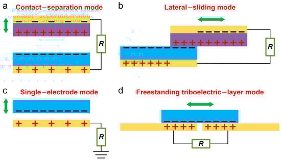
When the surfaces of two dissimilar materials were separated by mechanical force, the electrostatic charges generated by their physical contact could generate a potential drop. It could drive electrons to flow between the two electrodes on the top and bottom surfaces of the two materials. TENGs based on the above theory have four basic modes
[142][167]: the contact–separation mode, the lateral–sliding mode, the single–electrode mode, and the freestanding triboelectric–layer mode, as elaborated in
Figure 12a–d, respectively. Generally speaking, physical contact between the two dielectric films creates oppositely charged surfaces. During the regular relative motion between dielectric layers and electrodes, electrons are driven to continuously transfer alternately between the electrode and electrode or electrode and earth to form the AC output. To avoid the energy dissipation caused by the rectifier bridge and improve the practicality of TENG as a flexible energy–harvesting and self–powered sensing device, DC-TENGs based on different mechanisms with various materials properties were developed.
Figure 12. Four basic working modes of TENGs. (a) The contact–separation mode. (b) The lateral–sliding mode. (c) The single–electrode mode. (d) The freestanding triboelectric–layer mode.
2.2. DC-TENGs Based on Dielectric Materials
2.2.1. Mechanical Rectification
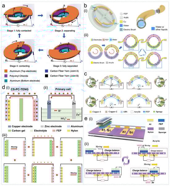
DC-TENGs based on dielectric materials can be obtained by the current commutation units, in which the alternating contact with the electrode is ensured to realize the mechanical rectification. It is equivalent to continuously exchanging the position between two electrodes as the direction of electron flow changes, ensuring the unidirectional flow of charge carriers between the two current commutation units. In 2014, a rotating–disk–based DC-TENG
[143][166] was reported by Zhang et al. shown in
Figure 23a, in which two pairs of parallel flexible electric brushes were designed as the current commutation units. During the operation of the DC-TENG, as the top friction electrode (aluminum, Al) continued to rotate, it constantly contacted and separated from the dielectric layer (polyvinyl chloride, PVC), driving electrons to alternately transfer between the top friction electrode and the bottom charge–collecting electrode (Al) to generate AC output. In the second half cycle of the generated AC signal, the contact relationship between the two pairs of electric brushes and the electrodes was exchanged. So the current direction between the two electric brushes was converted to the same direction as the first half cycle to generate the DC output. The peak power density of the DC-TENG reached 25 mW/m
2 at the rotating speed of 750 r/min. In the kind of DC-TENG with the electric brush as the commutation unit, the friction and wear between brush and electrode is an important factor affecting the stability of device operation. To deal with this problem, the carbon fiber material was selected to make the flexible electric brush in the rotating–disk–based DC-TENG. Converting the fixed sliding friction between electric brushes and electrodes to free sliding friction was another effective way to reduce friction and wear, as rotary–tubular DC-TENG was reported by Wang et al. in 2019
[144][168]. Its prototype structure was mainly composed of a fluorinated ethylene propylene (FEP) ring tube and copper (Cu) charge–collecting electrodes as shown in
Figure 23b(i). When the DC-TENG started to operate, the pre–filled liquid was in full contact with the tube, and the negative charge in the liquid was transferred to the inner surface of the tube. As the device continued to rotate, Cu electric brushes fixed on both sides of the tube alternately swept across the surface of charge–collecting electrodes to ensure that the current direction between brushes remained unchanged, forming the DC output [
Figure 23b(ii)]. In this DC-TENG, not only the free sliding mode was used to effectively reduce the friction and wear between the electric brushes and the charge–collecting electrodes, but also the use of liquid friction materials could completely avoid faster friction and wear between solid materials. Furthermore, in terms of friction reduction, rolling friction is undoubtedly better than sliding friction. In 2021, Qiao et al. reported a bidirectional DC-TENG
[145][169] (
Figure 23c), in which the rolling electric brushes were used as the current commutation units. During the operation of DC-TENG, the electric brushes alternately rolled through the friction electrode surfaces, which made the equipment produce DC output and effectively reduce friction and wear between the electric brushes and friction electrode to improve durability. In addition, the FEP dielectric layer was designed to the arched structure, which allowed the DC-TENG can harvest efficiently bidirectional rotating mechanical energy. At the rotation speed of 180 r/min, it could obtain a peak output power of 0.96 W/m
2.
Figure 23. DC-TENGs based on mechanical rectification. (
a) The rotating–disk–based DC-TENG was reported by Zhang et al. in 2014
[143][166]. (
b) The rotary–tubular DC-TENG based on liquid–dielectric contact was designed by Wang et al. in 2019
[144][168]—(
i) the schematic diagram of the rotary–tubular DC-TENG; (
ii) the operating principle display. (
c) The bidirectional DC-TENG based on the rolling electric brush structure was invented by Qiao et al. in 2021
[145][169]. (
d) The DC-TENG based on the mechanical delay switch design was reported by Fu et al. in 2022
[146][170]—(
i) the schematic diagram of the DC-TENG; (
ii) the DC-TENG was analog to the primary battery; (
iii) the operating principle display. (
e) The high–performance DC-TENG based on the mechanical delay switch and blank–tribo–area was invented by Du et al. in 2022
[147][171]—(
i) the schematic diagram of the DC-TENG; (
ii) the operating principle display.
In addition to the electric brushes, the time–delay switches could also be used as the current commutation units of DC-TENG. For example, Fu et al. invented a DC-TENG inspired by the primary battery in 2022
[146][170] [
Figure 23d(i)]. Analog to the cathode and anode electrodes in the primary battery shown in
Figure 23d(ii), the DC-TENG was mainly composed of three parts: negative and positive charge–collecting electrodes, and conductive carbon gel. In the device, the ability of FEP, carbon gel, and nylon to obtain electrons decreases in turn based on the difference in electronegativity. The specific operating mechanism was shown in
Figure 23d(iii). The carbon gel first contacted the left nylon dielectric layer and adsorbed electrons on the gel surface. Next, it contacted the right FEP dielectric layer to generate a displacement current in the external circuit, and then the time–delay switch between the carbon gel and the right charge–collecting electrode was turned on to generate a conduction current from the electrode to the gel, making the carbon gel positively charged. When it contacted the left nylon dielectric layer again, the displacement current in the same direction was generated again in the external circuit. Then, the time–delay switch between the carbon gel and the left charge–collecting electrode was turned on to generate a conduction current from the electrode to the gel, and it made the carbon gel negatively charged again. Therefore, as the carbon gel moved alternately between the left and right charge–collecting electrodes, DC-TENG continued to operate stably. The design of the time–delay switch as the current commutation unit completely avoided the friction and wear between electric brushes and electrodes in DC-TENG from mechanical rectification. Based on the similar current commutation unit, Du et al. developed a high–performance DC-TENG in 2022
[147][171] [
Figure 23e(i)]. During the operation, as the slider composed of an FEP dielectric layer and a charge–collecting electrode slid on the upper surface of the fixed nylon dielectric layer, the time–delay switch regularly closed and disconnected, prompting the one–way flow of electrons between the two charge–collecting electrodes on the stator lower surface to generate the DC output, as demonstrated in
Figure 3e(ii). Particularly, the blank–tribo–area was designed in the DC-TENG, which could increase power output by promoting charge accumulation. When the DC-TENG was designed as a disk structure, the open–circuit voltage, short–circuit current, and peak power could reach 3000 V, 106.9 μA, and 75.69 mW, respectively, at the excitation speed of 60 r/min.
2.2.2. Phase Coupling
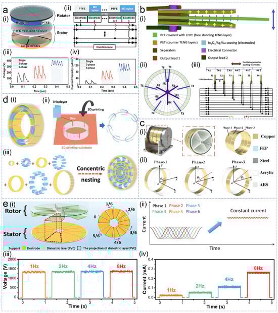
Although DC-TENGs from mechanical rectification could generate DC output without the assistance of the rectifier bridge, the current signals were generally pulsed with a high crest factor, which cannot constantly power electronics. To further reduce the crest factor of the DC signal and enable the device to achieve more stable output, the principle of phase coupling began to be explored. Ryu et al. invented a multiphase rotating DC-TENG in 2018
[148][145] [
Figure 34a(i)], in which the rotator was made of alternating polytetrafluoroethylene (PTFE) and nylon dielectric layers, and the stator was composed of PTFE dielectric layers and charge–collecting electrodes on its lower surface. In the physical structure of DC-TENG, by adjusting the quantitative relationship between the dielectric layers in the rotor and the charge–collecting electrodes in the stator, a regular phase difference was constructed between them. The charge–collecting electrodes were connected according to the equivalent rectifier circuit shown in
Figure 34a(ii). During the operation of the DC-TENG, as the rotor continued to rotate, each charge–collecting electrode generated a similar AC signal with the regular phase difference. These AC signals were converted into constant DC signals by the equivalent rectifier circuit, including the constant open–circuit voltage and constant short–circuit current, as shown in
Figure 34a(iii,iv). Experiments showed that with the increase in the number of phases, the output was more stable, and the crest factor was closer to 1. When the phase number was 5, the current crest factor of the multiphase rotating DC-TENG was 1.26. In addition to the sliding mode DC-TENG from phase coupling, the constant output could also be achieved by using multiple contact–separation mode TENGs, as Dharmasena et al. developed the DC-TENG in 2020
[149][172] [
Figure 34b(i)]. In the DC-TENG, multiple contact–separated TENGs were installed in the device shell according to the regular angle difference [
Figure 34b(ii)], and they were connected to the equivalent rectifier circuit in the way shown in
Figure 34b(iii). Each contact–separated TENGs could generate similar AC electrical signals with regular phase differences when they were sequentially excited, which was finally converted into a constant output by the equivalent rectifier circuit. After testing, the current crest factor of this contact-mode DC-TENG with six phases was 1.08 at an oscillation frequency of 5 Hz.
Figure 34. The DC-TENG based on phase coupling. (
a) The multiphase rotating DC-TENG was invented by Ryu et al. in 2018
[148][145]—(
i) the schematic diagram of the multiphase rotating DC-TENG; (
ii) the charge–collecting electrodes were connected according to the equivalent rectifier circuit; (
iii,
iv) the effect of the number of phases on the output performance. (
b) The contact–mode DC-TENG was developed by Dharmasena et al. in 2020
[149][172]—(
i) the schematic diagram of the contact–mode DC-TENG; (
ii) multiple contact-separated TENGs were installed in the device shell according to the regular angle difference in the DC-TENG; (
iii) multiple contact–separated TENGs were connected according to the equivalent rectifier circuit. (
c) The cylindrical DC-TENG was designed by Wang et al. in 2020
[150][173]—(
i) the schematic diagram of the cylindrical DC-TENG; (
ii) the same phase difference between the different phases of the DC-TENG. (
d) The DC-TENG with a low current crest factor was reported by Hu et al. in 2021
[151][174]—(
i) the schematic diagram of the DC-TENG; (
ii) the bracket for installing the dielectric layer was processed by 3D digital printing technology in the DC-TENG; (
iii) the nested DC-TENG array was designed by the coaxial superposition of multiple stators and rotors to effectively improved the space utilization and output performance. (
e) The constant–voltage DC-TENG was invented by Li et al. in 2022
[152][175]—(
i) the schematic diagram of the constant–voltage DC-TENG; (
ii) the AC signals generated by different phases were integrated into the approximate constant DC signals; (
iii,
iv) the influence of operating frequency on open–circuit voltage and short–circuit current of the DC-TENG.
The regular phase difference is the basis for the DC-TENG from phase coupling, so how to design an accurate regular phase difference becomes critical to affecting the stability of the device. In 2020, Wang et al. reported a cylindrical DC-TENG
[150][173], which consisted of multiple TENGs with a regular phase difference as shown in
Figure 34c(i). Different from the complex design of the regular phase difference in the conventional DC-TENGs from phase coupling, as long as the same angle difference was guaranteed between each TENG shown in
Figure 34c(ii), the regular phase difference could be guaranteed. So, it undoubtedly effectively reduced the complexity. Experiments showed that with the increase in the number of friction electrode groups in each TENG, the constant short–circuit current of the DC-TENG output was increased. In the DC-TENG with three phases and five groups, the short–circuit current could reach 21.6 μA, and the current crest factor remained at 1.08. To further ensure the accuracy of the designed regular phase difference, Hu et al. also reported a low crest factor DC-TENG
[151][174], as shown in
Figure 34d(i). In the DC-TENG, the bracket for installing the dielectric layer was processed by 3D digital printing technology exhibited in
Figure 34d(ii), which effectively controlled the accuracy of the regular phase difference. On this basis, the crest factor of the DC-TENG was reduced to 1.07 at the rotation speed of 8 r/s. In particular, a nested DC-TENG array was designed by the coaxial superposition of multiple stators and rotors, which effectively improved the space utilization and output performance [
Figure 34d(iii)]. The nested DC-TENG array obtained a constant short–circuit current of 140 μA at 8 r/s, which was 1.7–fold higher than that of a single stator. Compared with the pulse output method, DC-TENG with constant output had a higher average power density, as in 2022, Li et al. reported a constant–voltage DC-TENG
[152][175] shown in
Figure 34e(i), which achieved better output performance based on the phase coupling principle [
Figure 34e(ii)]. When the rotation frequency was 8 Hz, it could achieve a constant voltage output of 1400 V [
Figure 4e(iii)] and a constant current output of 0.26 mA [
Figure 34e(iv)], and the crest factor of the voltage was reduced to 1.03. Compared with the 2.33 mW of pulsed TENG without regular phase difference, the average power of the constant–voltage DC-TENG reached 4.56 mW and was increased by 1.9 fold.
2.2.3. Dielectric Breakdown
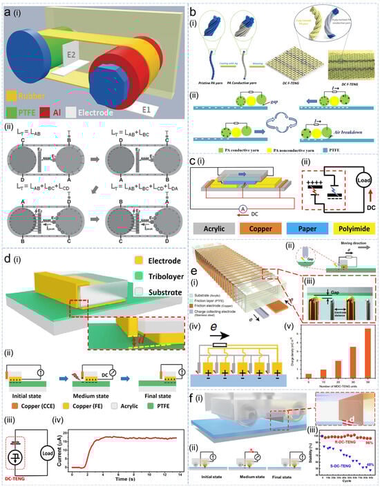
In addition to mechanical rectification and phase coupling, DC-TENG based on dielectric materials could also achieve constant DC output in a much simpler structure by the introduction of the electrostatic breakdown effect. In terms of pulsed DC output, Yang et al. developed a rotating DC-TENG based on the dielectric breakdown effect in 2014
[153][148], which consisted of two rotating wheels connected by a rubber belt [
Figure 45a(i)]. Its operating mechanism was shown in
Figure 45a(ii). During the DC-TENG operation, electrons on the surface of Al wheels were first transferred to the inner surface of the belt and then to the surface of PTFE wheels due to the difference in material electronegativity. The charge–collecting electrode surface continuously accumulated positive charges thanks to the electrostatic induction effect. When the electrostatic potential between charge–collecting electrode and the PTFE wheel reached the breakdown voltage, the air medium was broken down to produce pulse discharge, which would drive electrons from the charge–collecting electrode to the friction electrode, resulting in a DC pulse signal. It could generate an open–circuit voltage of approximately 3200 V at the rotation speed of 1000 r/min, so the DC-TENG from the dielectric breakdown was an important means to produce a high voltage output. In addition to rigid physical devices, DC-TENG from dielectric breakdown could also operate normally when it was made into wearable fabrics as a flexible energy–harvesting device. In 2020, Chen et al. developed a fabric DC-TENG
[154][176], which used flexible conductive yarn to generate the dielectric breakdown effect to harvest biological motion energy [
Figure 45b(i)]. As demonstrated in
Figure 45b(ii), when the fabric slid forward on the PTFE dielectric surface, the left yarn as the friction electrode contacted the dielectric layer and transferred electrons to the dielectric layer surface. Then, the fabric moved in the opposite direction, based on the electrostatic induction effect, and the right yarn as the charge–collecting electrode continued to accumulate positive charges on the surface. When the electrostatic breakdown occurred between the charge–collecting electrode and the dielectric layer, the breakdown current drove electrons to flow unidirectionally between the friction electrode and the charge–collecting electrode to generate the DC pulse output. A small fabric DC-TENG (15 mm × 35 mm) could generate an open–circuit voltage of 4500 V, which was enough to light more than 400 light–emitting diodes (LEDs). The rapid accumulation of charge density on the surface of the charge–collecting electrode was an important factor in the dielectric breakdown effect. Compared with the CE between metal and dielectric materials, there was no doubt that the two dielectric materials with greater electronegativity difference have more electron transfer and faster potential difference growth during contact. So, Li et al. developed a dual–breakdown DC-TENG in 2022
[155][177], which uses dielectric materials with different electronegativity as friction materials shown in
Figure 45c(i). As shown in the equivalent circuit of
Figure 45c(ii), the DC-TENG consisted of two dielectric materials as charge sources and corresponding charge–collecting electrodes. When the two dielectric layers contacted each other, based on the difference in material electronegativity, an equal amount of different electric charges was generated on their contact surfaces. When they were separated from each other, electrostatic breakdown effects were generated between them and the corresponding charge–collecting electrodes to exert a synergistic enhancement effect. It led to the unidirectional flow of electrons in the external circuit between the two charge–collecting electrodes, resulting in a synergistic pulsed DC output.
Figure 45. DC-TENGs based on the dielectric breakdown. (
a) The rotating DC-TENG was developed by Yang et al. in 2014
[153][148]—(
i) the schematic diagram of the rotating DC-TENG; (
ii) the operating principle of the DC-TENG. (
b) The fabric DC-TENG was invented by Chen et al. in 2020
[154][176]—(
i) the schematic diagram of the fabric DC-TENG; (
ii) the operating principle display. (
c) The dual–breakdown DC-TENG was reported by Li et al. in 2022
[155][177]—(
i) the schematic diagram of the dual–breakdown DC-TENG; (
ii) the electrical mode of DC-TENG. (
d) The constant current DC-TENG was designed by Liu et al. in 2019
[156][178]—(
i) the schematic diagram of the constant current DC-TENG; (
ii) the working principle of the DC-TENG; (
iii) the electrical mode of DC-TENG; (
iv) the constant open–circuit voltage output from the DC-TENG. (
e) The DC-TENG with ultra–high surface charge density was invented by Zhao et al. 2020
[157][179]—(
i) the schematic diagram of the DC-TENG; (
ii) the working principle display; (
iii) the output performance of the DC-TENG was effectively improved by the rationally patterned structure design of the friction electrode and charge–collecting electrode; (
iv) the parallel connection of multiple output units of the DC-TENGs; (
v) the charge density of the DC-TENGs reached 5.4 mC/m
2. (
f) The robust rolling–mode DC-TENG was developed by Gao et al. in 2021
[158][180]—(
i) the schematic diagram of the rolling–mode DC-TENG; (
ii) the working principle display; (
iii) the rolling operation method effectively reduced the friction and wear and improved the stability of DC-TENG.
In DC-TENG from dielectric breakdown, constant electric signals also could be generated. Liu et al. invented a constant current DC-TENG in 2019
[156][178] [
Figure 45d(i)], and its working mechanism was shown in
Figure 45d(ii). When the Cu friction electrode contacted the PTFE dielectric layer, its electrons on the surface were transferred to the dielectric layer surface. As the slider slid forward, under the electrostatic induction of electrons on the surface of the dielectric layer, positive charges gradually accumulated on the charge–collecting electrode surface. In this kind of DC-TENG, the equivalent model consisted of a charge source together with a breakdown capacitor [
Figure 45d(iii)], and the continuous unidirectional dielectric breakdown in the capacitor caused the DC-TENG to produce the constant output between the friction electrode and the charge–collecting electrode [
Figure 45d(iv)]. The DC-TENG could obtain a higher charge density of approximately 430 μC/m
2, which was much higher than that of conventional TENG. To further explore the effective way to achieve higher performance of this kind of DC-TENG, Zhao et al. proposed a patterned electrode optimization method in 2020
[157][179], which could achieve ultra–high surface charge density output, as shown in
Figure 45e(i). Based on the similar dielectric breakdown mechanism shown in
Figure 45e(ii), the output performance of the DC-TENG was effectively improved by the rationally patterned structure design of the friction electrode and charge–collecting electrode [
Figure 45e(iii)]. The parallel connection of multiple output units was shown in
Figure 45e(iv). Its charge density reached 5.4 mC/m
2 [
Figure 45e(v)], which was more than 10 fold that of conventional DC-TENG. In DC-TENG based on dielectric materials, friction and wear between materials have always been important factors affecting stable output. To effectively solve such problems, Gao et al. designed a robust rolling–mode DC-TENG
[158][180] [
Figure 45f(i)]. As shown in
Figure 45f(ii), the planar friction electrode was converted into the roller structure in the DC-TENG, which converted the sliding friction between the friction electrode and the dielectric layer into rolling friction while enabling the device to achieve constant current output. It effectively reduced the friction and wear and improved the stability of DC-TENG, as shown in
Figure 45f(iii). According to the analysis of DC-TENG based on dielectric materials, high voltage output characteristics due to the insulation characteristics of the dielectric materials would effectively broaden the practical application field of the TENG.
2.3. DC-TENGs Based on Semiconductor Materials
In DC-TENGs based on dielectric materials, the insulation characteristics of the dielectric layer caused higher internal resistance, which would reduce the short–circuit current density and its energy supply for electronic devices. To effectively improve the current density of the DC-TENGs, they could be combined with the electromagnetic or piezoelectric nanogenerator. However, such hybrid nanogenerators
[159][160][161][162][181,182,183,184] inevitably led to the complexity of the device structure and affected its robustness. In particular when the internal resistance between different types of generators was not in the same order of magnitude, it resulted in unsatisfactory output performance. To effectively reduce the internal resistance of TENG to increase the output current, DC-TENG based on semiconductor materials had been developed. The DC output was realized based on the tribovoltaic effect between different types of friction materials, which was mainly divided into four types—semiconductor–semiconductor contact, metal–semiconductor contact, metal/semiconductor–insulator–metal/semiconductor contact, and liquid–semiconductor contact.
2.3.1. Semiconductor–Semiconductor Contact
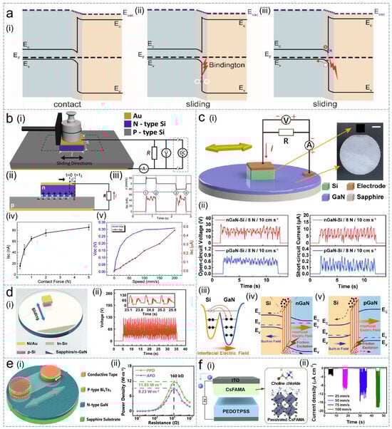
The tribovoltaic effect generated by the sliding of the semiconductor materials could directly generate constant signals
[163][150], and the specific output mechanism was shown in
Figure 56a. When the p–type silicon (Si) and n–type Si were in contact with each other, based on the Fermi energy level difference, electrons were transferred from n–type semiconductors to p–type semiconductors, and holes were transferred in the opposite direction. So, a built–in electric field in the direction from the n–type semiconductor to the p–type semiconductor was generated at the contact surface to form a p–n junction, as demonstrated in [
Figure 56a(i)]. When the relative motion occurred between the two semiconductors, the atoms on the two surfaces interacted to form the new chemical bonds and release the frictional energy (“Bindington”) [
Figure 56a(ii)]. The frictional energy (“Bindington”) in the tribovoltaic effect was similar to the role of the excitions in the photovoltaic effect, which excited the electron–hole pair at the contact interface to move along/against the built–in electric field, thereby forming the constant output in the external circuit [
Figure 56a(iii)]. Based on this principle, Xu et al. reported a DC-TENG based on the mutual sliding between p-n type Si in 2019
[164][151], as shown in
Figure 56b(i). Experiments showed that in the tribovoltaic effect between the two, the direction of the constant current was the same as that of the built-in electric field [
Figure 56b(ii)] and was independent of the relative sliding direction [
Figure 56b(iii)]. During the DC-TENG operation, as the contact force between semiconductors increased, they were contacted more fully so that the output performance was increased [
Figure 56b(iv)]. Similarly, as the relative sliding speed increased, the transfer speed of charge carriers in DC-TENG continued to increase, so the short–circuit current was increased, as shown in
Figure 56b(v).
Figure 56. The DC-TENG based on the semiconductor–semiconductor contact. (
a) Energy band diagrams during the sliding of the p–type semiconductor and the n–type semiconductor were reported by Lin et al. in 2023
[163][150]—(
i) the built–in electric field in the direction from the n–type semiconductor to the p–type semiconductor was generated at the contact surface to form a p–n junction; (
ii) when the relative motion occurred between the two semiconductors, the atoms on the two surfaces interacted to form the new chemical bonds and release the frictional energy (“Bindington”); (
iii) The frictional energy excited the electron–hole pair at the contact interface to move along/against the built–in electric field, thereby forming the constant output in the external circuit. (
b) The DC-TENG based on the mutual sliding between p–n type Si was developed by Xu et al. in 2019
[164][151]—(
i) the schematic diagram of the DC-TENG; (
ii) the working principle of the DC-TENG; (
iii) the output signals of the DC-TENG was independent of the relative sliding direction; (
iv,
v) the influence of contact pressure and relative sliding speed on output performance. (
c) The gallium nitride–based DC-TENG was invented by Chen et al. in 2022
[165][185]—(
i) the schematic diagram of the DC-TENG; (
ii) the output performance when the Si was sliding relative to n–type GaN and p–type GaN, respectively; (
iii) the CE effect between Si and GaN; (
iv,
v) the energy band diagrams when the Si was sliding relative to n–type GaN and p–type GaN, respectively. (
d) The DC-TENG with an ultra–high voltage output was designed by Wang et al. in 2022
[166][186]—(
i) the schematic diagram of the DC-TENG; (
ii) the open–circuit voltage of the DC-TENG. (
e) The DC-TENG with ultra–high power density was developed by Li et al. in 2022
[167][187]—(
i) the schematic diagram of the DC-TENG; (
ii) the peak power density of the DC-TENG. (
f) The high–performance DC-TENG based on n–type perovskite (CsFAMA) and p–type conductive polymer (PEDOT: PSS) was invented by Lee et al. in 2023
[168][188]—(
i) the schematic diagram of the high–performance DC-TENG; (
ii) the influence of relative sliding speed on output performance.
When the different types of semiconductors were in contact with each other to form heterojunctions, the constant current output could also be generated based on the tribovoltaic effect between the two. Chen et al. developed a DC-TENG based on the mutual sliding between gallium nitride (GaN) and Si in 2022
[165][185] shown in
Figure 56c(i). Experiments showed that when the n–type and p–type GaN slid on the Si surface, respectively, the direction of the generated voltage or current was the same and the amplitude was not equal, as demonstrated in
Figure 56c(ii). It indicated that the direction of the generated current might not depend only on the direction of the built–in electric field between different types of semiconductors. After analysis, when different types of semiconductors contacted each other, in addition to the built–in electric field thanks to heterojunction, based on the difference in electronegativity, the interface electric field generated by the CE between the two played a stronger role [
Figure 56c(iii)]. As shown in
Figure 56c(iv), when n–type GaN and Si contacted each other, the two electric fields were in the same direction, and the superposition of the two effectively increased the output performance of DC-TENG. When p–type GaN contacted Si, the two electric fields were in opposite directions, and their mutual suppression weaken the output performance of DC-TENG [
Figure 56c(v)]. Therefore, the DC-TENG based on the contact of different types of semiconductor materials could produce higher output under the superposition of the built–in electric field and the interface electric field. When the sliding speed of the DC-TENG was 10 cm/s, the open–circuit voltage reached 25 V and the short–circuit current density reached 0.1 A/m
2. Based on a similar power generation principle, Wang et al. constructed a high–voltage DC-TENG based on the contact of n–type GaN and p–type Si in 2022
[166][186], as shown in
Figure 56d(i). In the DC-TENG, under the combined action of a built–in electric field and interface electric field, the open–circuit voltage was up to 130 V, which was approximately 20 fold that of conventional semiconductor–based TENG [
Figure 56d(ii)]. Its peak power density reached 2.8 W/m
2, which was approximately 46 fold that of the conventional centimeter–level semiconductor-based TENG. To further improve the power density, in 2022, Zhang et al. developed DC-TENG based on the contact between the p–type bismuth telluride (Bi
2Te
3) and n–type GaN
[167][187], as shown in
Figure 56e(i). Under the combined action of a strong interface electric field and a built–in electric field, its average power density reached 9.23 W/m
2 shown in
Figure 56e(ii), which was several orders of magnitude higher than that of conventional TENG based on semiconductor materials. The tribovoltaic effect also occurred between the organic polymer and the inorganic semiconductor. In 2023, Lee et al. invented a high–performance DC-TENG based on n–type perovskite (CsFAMA) and p–type conductive poly(3,4–ethylenedioxythiophene): poly(styrene sulfonate) (PEDOT: PSS)
[168][188] as shown in
Figure 56f(i). In the DC-TENG, the internal defect of CsFAMA was passivated by choline chloride (ChCl) to improve the charge density and carrier mobility, so that the short–circuit current density reached 11 μA/cm
2 shown in
Figure 56f(ii).
2.3.2. Metal–Semiconductor Contact
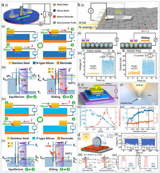
There was a wide choice of friction materials in the tribovoltaic effect. In addition to the p–n junction between semiconductor–semiconductor materials, the DC-TENG based on the Schottky junction between metal–semiconductor materials could also achieve the DC output. In 2020, Zhang et al. invented low–impedance DC-TENG based on the contact between stainless steel metal and Si semiconductor
[169][154] [
Figure 67a(i)], and the specific working mechanism was shown in
Figure 67a(ii). The Schottky junction was constructed when the stainless steel with a large work function was in static contact with the n–type Si with a small work function, and electrons transferred from the semiconductor side to the metal side, forming a built–in electric field. Then, the friction energy released by the formation of atomic bonds during the sliding process of the metal on the semiconductor surface could excite non–equilibrium carriers, which included the excited electron–hole pairs in the semiconductor space charge region and the excited electron composition of the metal and semiconductor surface states. Under the action of the built–in electric field, the non–equilibrium carriers could drift along or against the direction of the built–in electric field, generating constant output in the external circuit. Correspondingly, the energy band diagram between the stainless steel and n–type Si was shown in
Figure 67a(iii) at different operating stages of the DC-TENG. On the other hand, when the stainless steel and p–type Si slid with each other [
Figure 67a(iv)], electrons transferred from the metal side to the p–type Si side, and a reverse built–in electric field was constructed, due to a higher work function and a lower Fermi level of p–type Si. With the relative sliding of stainless steel and p–type Si, the reverse built–in electric field drove the electrons to flow unidirectionally in the external circuit to generate reverse DC output, and the change process of the energy band diagram was shown in
Figure 67a(v). The tribovoltaic effect could also occur when the metal and the flexible organic semiconductor polymers slide relatively. In 2021, Meng et al. proposed a flexible textile DC-TENG based on the contact between the metal Al and the conducting polymer PEDOT
[170][189], as shown in
Figure 67b(i). In this DC-TENG, The direction of the built–in electric field was from Al to PEDOT, which drove the non–equilibrium carriers generated during the sliding process to move along or against the direction of the built–in electric field to generate constant output [
Figure 67b(ii)]. Through the way of increasing voltage in series and increasing current in parallel of multiple power generation units, the open–circuit voltage of 3.5V [
Figure 67b(iii)] and the short–circuit current of 70 μA [
Figure 7b(iv)] could be generated, respectively, by two integration methods from seven DC-TENGs.
Figure 67. The DC-TENG based on the metal–semiconductor contact. (
a) The low–impedance DC-TENG was invented by Zhang et al. in 2020
[169][154]—(
i) the schematic diagram of the low–impedance DC-TENG; (
ii,
iii) the working principle and the energy band diagram of the DC-TENG when the metal slider slid on the n–type Si surface; (
iv,
v) the working principle and the energy band diagram of the DC-TENG when the metal slider slid on the p–type Si surface. (
b) The flexible textile DC-TENG was proposed by Meng et al. in 2021
[170][189]—(
i) the schematic diagram of the flexible textile DC-TENG; (
ii) the working principle of the DC-TENG; (
iii,
iv) the output performance of the DC-TENGs with different connections modes. (
c) The superlubric DC-TENG was designed by Huang et al. in 2021
[171][190]—(
i,
ii) the schematic diagram and the optical microscopic image of the superlubric DC-TENG; (
iii) the peak power density of the DC-TENG; (
iv) the stability test of the DC-TENG. (
d) The rolling–mode DC-TENG was proposed by Yuan et al. in 2022
[172][191]—(
i) the schematic diagram and the working principle of the rolling-mode DC-TENG; (
ii) the stability test of the DC-TENG; (
iii) the change of energy band diagram during the operation of the DC-TENG; (
iv,
v) the effect of illumination on the output performance of DC-TENG.
Similar to DC-TENG based on the dielectric layer, rapid friction and wear between materials were also negative factors affecting the stability of DC-TENG based on semiconductor materials. To solve this problem effectively, a superlubric DC-TENG was invented by Huang et al. in 2021
[171][190] as shown in
Figure 67c(i), and its optical microscopic image was shown in
Figure 67c(ii). The DC output was generated based on the tribovoltaic effect between the graphite and the n–type Si. Due to the lubrication of graphite, it was in a super–lubrication state with the silicon surface, that is, ultra–low friction and wear–free state. Such DC-TENG could not only produce excellent short–current density (approximately 210 A/m
2) and peak power density (approximately 7 W/m
2) shown in
Figure 67c(iii), but also achieve stable operation of at least 5000 cycles. In particular, the output current and friction had no obvious attenuation [
Figure 67c(iv)], indicating that it could achieve longer stable operation. In addition to the application of anti–friction materials, the conversion of sliding friction to rolling friction can also effectively reduce friction and wear between materials. In 2022, Yuan et al. developed a rolling–mode DC-TENG
[172][191] as shown in
Figure 67d(i), which generated constant output based on the tribovoltaic effect between Al and all–inorganic perovskite (CsPbBr
3). In such DC-TENG, the friction and wear were significantly reduced, so that the device operated more stably and the output performance did not decrease significantly after more than 10 min of cycling [
Figure 67d(ii)]. Based on synergistic the photovoltaic effect of CsPbBr
3 and the tribovoltaic effect, the DC-TENG coupled the two effects to form the tribo–photovoltaic effect, as demonstrated in
Figure 67d(iii). Due to the excite electron–hole pairs from both effects, the output could be generated when the electric field directions were the same to effectively increase the output performance. Under illumination, the open–circuit voltage and short–circuit current density of DC-TENG reached 3.69 V and 11.46 A/m
2, respectively, as shown in
Figure 67d(iv,v).
2.3.3. Metal/Semiconductor–Insulator–Metal/Semiconductor Contact
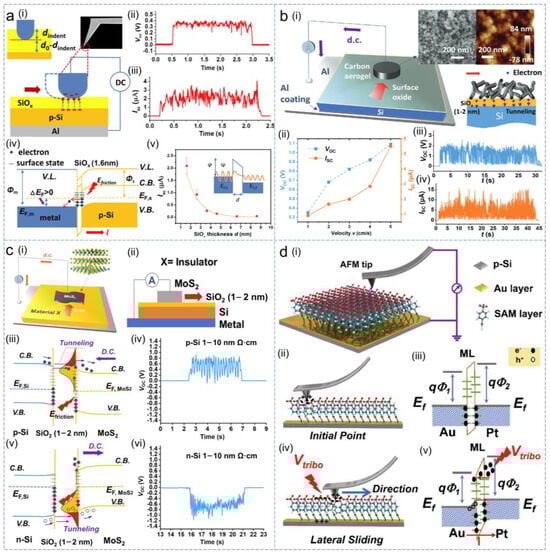
To further reduce the rapid friction and wear in DC-TENG based on semiconductor materials, a thin insulating layer was introduced between the semiconductor–semiconductor contact or metal–semiconductor contact to form the tribo–tunneling effect. In 2018, Liu et al. developed a DC-TENG based on metal–insulator–semiconductor contact
[173][157] shown in
Figure 78a(i). When the probe (platinum, Pt) of the electrical–atomic force microscopy contacted with the silicon oxide of p–type Si, under the action of Schottky junction, electrons tunneled through the insulating layer from the metal side with a high Fermi level to the semiconductor side with a low Fermi level, forming a built–in electric field. When the relative sliding occurs between the Pt and the insulating layer, the released friction energy stimulated the non–equilibrium carriers to tunnel through the insulating layer along or against the built–in electric field, driving a constant open–circuit voltage and short–circuit current generated as shown in
Figure 78a(ii,iii), and the energy band diagram between Pt and p–type Si was shown in
Figure 78a(iv). Experiments showed that the output performance of DC-TENG based on the tribo–tunneling effect decreased with the increase in insulating layer thickness due to the hindrance of the insulating layer to charge carriers, as shown in
Figure 78a(v). In this DC-TENG based on the AFM probe sliding on the insulating surface of the semiconductor, a high current density (1–10 A/m
2) was generated, but the manufacturing process of the probe was more complicated, and it could cause strong material wear. To solve such problems, Liu et al. proposed a DC-TENG based on the tribo–tunneling effect of carbon aerogel–insulator–semiconductor contact
[174][192] in 2019, as shown in
Figure 78b(i). The built–in electric field formed by the Schottky junction between carbon aerogel and p–type Si drove the charge carriers to tunnel through the insulating layer to form a constant output in the external circuit. Experiments showed that the open–circuit voltage and short–circuit current of the DC-TENG increased with the increase in relative sliding speed, as shown in
Figure 78b(ii). Particularly, based on the material properties of carbon aerogel, when it contacted the insulating layer, not only the friction and wear between the materials were effectively reduced, but also a large number of nano–contact points on the contact interface were constructed acting as the superposition of multiple power generation units to effectively improve the output performance of DC-TENG. The open–circuit voltage reached 2 V [
Figure 78b(iii)], short–circuit current reached 15 μA [
Figure 78b(iv)], and the theoretical current density reached 100 A/m
2.
Figure 78. The DC-TENG based on the metal/semiconductor–insulator–metal/semiconductor contact. (
a) The DC-TENG based on metal–insulator–semiconductor contact was developed by Liu et al. in 2018
[173][157]—(
i) the schematic diagram and working principle of the DC-TENG; (
ii,
iii) the open–circuit voltage and short–circuit current of the DC-TENG; (
iv) the energy band diagram of the DC-TENG, (
v) the effect of insulator thickness on output performance. (
b) prepared The DC-TENG based on the carbon aerogel–silicon oxide–p type silicon contact was proposed by Liu et al. in 2019
[174][192]—(
i) the schematic diagram and working principle of the DC-TENG; (
ii) the influence of relative sliding speed on the output performance of the DC-TENG; (
iii,
iv) the output performance of the DC-TENG. (
c) A class of DC-TENGs based on the MoS
2 material was constructed by Liu et al. in 2019
[175][193]—(
i,
ii) the schematic diagram of the DC-TENG; (
iii,
iv) the energy band diagram and the output of DC-TENG when the MoS
2 slid on the p–type Si surface; (
v,
vi) the energy band diagram and the output of DC-TENG when the MoS2 slid on the n–type Si surface. (
d) A high tunneling current DC-TENG based on the metal–insulator–metal contact was developed by Zhang et al. in 2023
[176][194]—(
i) the schematic diagram of the DC-TENG; (
ii,
iii) the DC-TENG was in the static contact state and the energy band diagram in this state, (
iv,
v) the DC-TENG was in the relative sliding state and the energy band diagram in this state.
In the tribo–tunneling effect, charge carriers could also be driven by p–n junctions between semiconductors to tunnel through the insulating layer. In 2019, Liu et al. constructed a class of DC-TENGs based on the molybdenum disulfide (MoS
2) material
[175][193] [
Figure 78c(i)], in which the DC output was realized based on the tribo–tunneling effect of MoS
2–SiO
2–Si contact [
Figure 78c(ii)]. When MoS
2 slid on the oxidized surface of p–type Si, the built–in electric field in the positive direction from MoS2 to p–type Si drove the charge carriers to tunnel through the SiO
2 insulating layer to form the constant output in the positive direction, as shown in
Figure 78c(iii,iv). When MoS
2 slid on the oxidized surface of n–type Si, the charge carriers were driven by the built–in electric field in the opposite direction to tunnel through the SiO
2 insulating layer to form the DC output, as demonstrated in
Figure 78c(v,vi). In addition to semiconductor materials, the tribo–tunneling effect could also occur between two metal materials, resulting in constant output. Zhang et al. developed a high tunneling current DC-TENG based on the metal–insulator–metal contact
[176][194] in 2023 [
Figure 78d(i)]. In this DC-TENG, the oligoacene 4–(trifluoromethyl)benzenethiol was grown on the gold electrode as a self–assembled monolayer (SAM) based on the strong electronegativity and outstanding lubricity. When the Pt probe was in static contact with the SAM layer, based on the electronegativity difference, electrons were transferred from the probe tip to the surface of the SAM layer [
Figure 78d(ii)], and the energy band diagram was shown in
Figure 78d(iii). In the sliding process of the probe, electrons tunneling through the SAM layer was generated under the synergistic effect of the interface potential difference and the tribovoltage generated by contact electrification to achieve a maximum constant short–circuit current density of 7.6 × 10
6 A/m
2 [
Figure 78d(vi)], with the energy band change shown in
Figure 78d(v).
2.3.4. Liquid–Semiconductor Contact
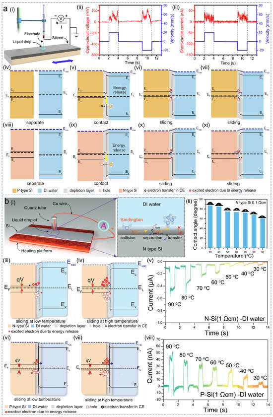
The tribovoltaic effect could also be generated between liquid and semiconductor, which could effectively reduce friction and wear. In 2020, Lin et al. invented a DC-TENG by driving droplets to slide on the Si surface
[177][160], as shown in
Figure 89a(i). When the deionized (DI) water droplets slid on the p–type silicon surface, the DC-TENG generated constant open–circuit voltage and short–circuit current, which was independent of the relative sliding direction [
Figure 89a(ii,iii)]. The Fermi level of water was higher than that of p–type Si, and when they were separated from each other, the energy band diagram was shown in
Figure 89a(iv). When the droplet contacted the p–type Si, the electrons were transferred from the droplet to the Si surface, forming a built–in electric field. At the same time, new chemical bonds might be formed at the contact interface, and the energy band diagram was shown in
Figure 89a(v). Electrons transfer and the formation of new chemical bonds both led to the release of friction energy at the contact interface, which could excite the generation of electron–hole pairs on the p–type Si surface [
Figure 89a(vi)]. Under the action of the built–in electric field, the electron–hole pairs would transfer along/against the electric field direction, forming the constant output in the external circuit [
Figure 89a(vii)]. When the DI water droplet contacted with n–type Si with a higher Fermi level, the electrons were transferred from the Si surface to the droplet, forming a reverse built–in electric field. It drove the electron–hole pairs to perform directional motion to form a reverse constant output, and the energy band diagrams at different operating stages were shown in
Figure 89a(viii–xi).
Figure 89. The DC-TENG based on the liquid and semiconductor contact. (
a) The DC-TENG by driving droplets to slide on the Si surface was invented by Lin et al. in 2020
[177][160]—(
i) the experimental test system of the DC-TENG; (
ii,
iii) the output of DC-TENG was independent of the flow direction of water droplets; (
iv–
vii) the energy band change diagram when the droplet slid on the p–type Si surface, (
viii–
xi) the energy band change diagram when the droplet slid on the n–type Si surface. (
b) The effect of temperature on the tribovoltaic effect at the liquid–semiconductor interface has been studied by Zheng et al. in 2021
[178][195]—(
i) the experimental test system; (
ii) the effect of temperature on the hydrophilicity of liquid; (
iii–
v) the energy band change diagram when the droplet slid on the n–type Si surface and the effect of temperature on output performance, (
vi–
viii) the energy band change diagram when the droplet slid on the p–type Si surface and the effect of temperature on output performance.
Furthermore, Zheng et al. studied the effect of temperature on the performance of DC-TENG based on the liquid–semiconductor contact
[178][195], as shown in
Figure 89b(i). As the temperature increases from 30 °C to 90 °C, the contact angle of DI water droplets on the Si surface decreases from 86.72 to 60.36° [
Figure 89b(ii)], which could increase the contact area of droplets on the Si surface to improve the output performance. When the DI water droplet was in contact with n–type Si, the electron–hole pairs density excited by the friction energy increased during the sliding process of the droplet and the n–type silicon surface as the temperature increased [
Figure 89b(iii, iv)]. It could effectively promote the output performance of the DC-TENG as shown in
Figure 89b(v). When the droplet was in contact with p–type Si, as the temperature increased, the reverse constant output was also improved, as demonstrated in
Figure 89b(vi–viii). According to the analysis of DC-TENG based on semiconductor materials, due to the material properties of semiconductors, it could effectively improve the output performance by reducing the internal resistance of the device to effectively increase the current density.
2.4. DC-TENGs Based on Materials for Iontronic Rectification
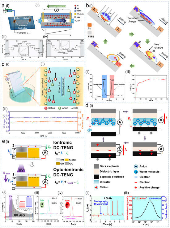
In DC-TENGs based on solid dielectric/semiconductor materials, the friction and wear between solid materials were an inevitable problem. The DC output mechanism formed by the unidirectional flow of ionic charge based on materials for iontronic rectification could avoid the above challenges. In 2015, Zhang et al. invented a microfluidic DC-TENG
[179][162] [
Figure 910a(i)], which could effectively convert liquid flow energy into constant electric output. When the 1 μmol/L KCl solution contacted the polydimethylsiloxane (PDMS) replica, based on the CE principle, the electrons were transferred from the liquid to the PDMS surface to form the electrical double layer (EDL), and the cation concentration was higher than that of the anion in the liquid. As the liquid was pushed through the PDMS surface, the net positive charge was transmitted to form the streaming current. The induced electric field generated by the charge distribution along the liquid flow direction led to the streaming potential, which drove the unidirectional flow of electrons in the external circuit to form the constant output, as shown in
Figure 910a(ii). As demonstrated in
Figure 910a(iii), with the continuous change in liquid flow rate, the amplitude of the short–circuit current generated by the DC-TENG altered accordingly. Once the flow direction of the liquid was changed, the direction of the output current altered accordingly, as shown in
Figure 910a(iv). To effectively improve the output performance of this type of DC generator, Dong et al. invented a high–voltage DC-TENG
[180][196] by using a pre–negative charged dielectric layer [
Figure 910b(i)]. In the falling process of the water droplet, the electric field constructed by negative charges on the PTFE dielectric layer drove the cations and anions in the water droplet to move along and against the electric field, respectively. When the droplet contacted the PTFE surface, the anions in the upper layer of the droplet contacted and transferred to the top Cu electrode, and it drove electrons to transfer from the top electrode to the bottom Cu electrode in the external circuit, forming the current Peak I. When the droplet slid along the dielectric layer and contacted with bottom electrode, the cations were transferred to the bottom electrode, which drove electrons to move in the same direction in the external circuit, forming the current Peak II. The two current signals in the same direction of DC-TENG were shown in
Figure 910b(ii). When the droplets were dropped at a frequency of 2.5 Hz, a constant voltage output of more than 1600 V could be generated in this high–voltage DC-TENG [
Figure 910b(iii)].To further achieve an effective constant output, Chi et al. developed a DC-TENG
[181][197] in 2022 [
Figure 910c(i)], which could produce constant electricity based on the action of water evaporation and capillary force. It consisted of a superhydrophilic porous aluminum oxide (Al
2O
3) ceramic sheet and electrodes arranged, respectively, at the top and bottom of the sheet. When the bottom electrode on the ceramic sheet was immersed in water, under the combined action of water evaporation and capillary force, the water continuously flowed upward along the nanopores inside the ceramic sheet and evaporated at the top of the sheet. In the process of liquid flow, electrons in water were transferred to the ceramic surface to form an EDL, and the net cations in the liquid continued to flow with the liquid to form a streaming current. It drove electrons to transfer from the top electrode to the bottom electrode to form the DC output in the external circuit, as shown in
Figure 910c(ii). Experiments showed that the DC-TENG could work normally only when the liquid could evaporate. It had stronger stability and could produce stable output (0.7 V and 0.3 μA) for at least 5000 s [
Figure 910c(iii)].
Figure 910. DC-TENGs based on materials for iontronic rectification. (
a) The microfluidic DC-TENG was invented by Zhang et al. in 2015
[179][162]—(
i) the schematic diagram of the microfluidic DC-TENG; (
ii) operation principle display; (
iii,
iv) the influence of liquid flow direction and velocity on output performance. (
b) The DC-TENG by using a pre–negative charged dielectric layer was developed by Dong et al. in 2021
[180][196]—(
i) the operation principle of the device; (
ii) two current signals caused by the sliding process of a single droplet; (
iii) the stable open–circuit voltage of the device. (
c) The DC-TENG based on the self–evaporation effect of water was designed by Chi et al. in 2022
[181][197]—(
i) the schematic diagram of the DC-TENG; (
ii) operation principle display; (
iii) the stable open–circuit voltage and short–circuit current of the DC-TENG. (
d) The DC-TING with efficient DC ionic-electronic coupling output was invented by Li et al. in 2023
[182][198]—(
i) the operation principle of the DC-TING; (
ii) the conversion process of DC-TING generating DC signals; (
iii) DC-TING achieved the ultra–high peak power density of 126.40 W/m
2 at 0.10 Hz. (
e) The opto–iontronic DC-TENG could be remotely replenished by UV light and was developed by Ouyang et al. in 2023
[183][199]—(
i) the operation principle of the opto–iontronic DC-TENG; (
ii) the influence of UV supplementation on the output performance of the device; (
iii,
iv) the DC-TENG could be used to perceive the light irradiation including UV light in the environment to realize the early warning protection function.
In DC-TENGs based on dielectric/semiconductor materials, the continuous attenuation of the surface charge density of the material is another challenge that affects the stability of the output performance. Even in DC-TENGs based on materials for iontronic rectification, the surface of the dielectric layer would gradually be covered with the EDL, which could prevent the electrons in the liquid from continuously transferring to its surface, invaliding the ionic rectification effect. To effectively avoid this challenge, Li et al. invented a direct–current triboiontronic nanogenerator (DC-TING) in 2023
[182][198], which could achieve efficient DC ionic–electronic coupling output [
Figure 910d(i)]. When the DC-TING was in a separate state, the pre–positive charged DI water was sprayed on the dielectric layer to form EDL. When the water film on the diffuse layer surface was contacted with the separate electrode, positive charges in the diffuse layer would be rapidly transferred onto the separate electrode surface, generating the ionic current
Ii. When the dielectric layer contacted the separate electrode, electrons from the separate electrode were transferred to the dielectric layer surface. When the dielectric layer was separated from the separate electrode, electrons from the back electrode were transferred to the separate electrode to generate the electronic displacement current
Ie.
Ii and
Ie were in the same direction and DC ionic–electronic coupling output was generated by the DC-TING. Experiments show that when the pre–charged DI water was sprayed onto the PTFE film, DC-TING started to output the short–circuit current in DC form [
Figure 910d(ii)]. As the ionic charge accumulated, the short–circuit current continued to increase to approximately 6.0 μA. DC-TING as a triboiontronic device based on the in situ ionic charge supplement strategy could maintain a high charge density on the dielectric insulator. It achieved the ultra–high peak power density of 126.40 W/m
2 at 0.10 Hz [
Figure 910d(iii)]. Similarly, to achieve the charge supplementation, the opto–iontronic DC-TENG
[183][199] was developed by Ouyang et al. in 2023, its ionic charge could be remotely replenished by UV light to maintain effective DC output [
Figure 910e(i)]. Based on the TENG structure, the unidirectional
Ii provided by the graphene oxide (GO)/reduced graphene oxide (rGO, containing K
+) junction was introduced to realize the rectification by counteracting
Ie generated by TENG in the opposite direction. Hence, the electronic–ionic coupling presented a DC current in the external circuit. However, the gradient balance of K
+ would cause
Ii to decay to a certain threshold (defined as
I’
i), which could not achieve the rectification effect on
Ie. At this point, the built–in electric field (
Ebulit) could be generated by irradiating rGO with a UV light source to construct a new ion concentration gradient and enhance the ionic current. The current generated by the UV was defined as
Ibulit, and the opto–iontronic strategy could achieve the sustainable rectification of the ionic current to the electronic current. Experiments have demonstrated that UV supplementation had an outstanding effect on maintaining the DC output of the device [
Figure 910e(ii)]. The opto–iontronic DC-TENG could be used to perceive the light irradiation including UV light in the environment to realize the early warning protection function. After the ion concentration balance, an AC signal would be presented, which was set to the ‘Calm’ state [
Figure 910e(iii)]. When the GO/rGO junction was irradiated by UV, the current signal transferred from AC signal to DC signal. At this time, it becomes an ‘Alarm’ state and warns against UV irradiation [
Figure 910e(iv)].
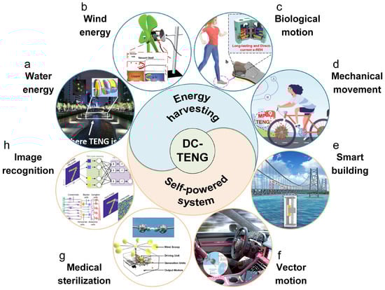
3. Various Applications of DC-TENGs
The advantages and disadvantages of DC-TENGs based on different material types have been summarized. To show them more intuitively, a comparison
Table 1 was constructed. Based on these advantages, DC-TENGs had a wide range of application fields in energy–harvesting and the self–powered system, as shown in
Figure 110. The mechanical energy from water, wind, biological motion, mechanical movement, raindrops, and many others could be effectively harvested by DC-TENGs. In 2018, Lim et al. designed a DC-TENG
[184][200] based on the phase coupling principle, which could effectively harvest the water flow energy with the assistance of the propeller to drive the LED board to operate normally [
Figure 101a]. Its practical application in the natural river environment proved that the TENG has good environmental adaptability and operational stability. In terms of wind energy harvesting, Yu et al. developed a DC-TENG based on the tribovoltaic effect between the Cu and p–type Si
[185][201] in 2021 [
Figure 110b]. It could output a constant current with an average of 4.4 mA (the maximum value was 8.4 mA), several orders of magnitude over previous generators based on the metal and semiconductor contact. In addition to natural resources, to effectively collect biological movement energy, Tao et al. developed a DC-TENG from the phase coupling
[186][202] in 2023 shown in [
Figure 110c]. Due to the advantages of the lightweight and small size of TENG, it could be installed in shoes to convert the low–frequency motion energy of the human walking into an approximately constant output with an average power of approximately 3.95 mW for supplying the micro biosensors. In addition, DC-TENG also could effectively harvest the mechanical movement energy widely existing in human life, such as vehicle operation and mechanical vibration. In 2021, the DC-TENG based on the phase coupling principle developed by Chen et al.
[187][203] [
Figure 110d], which was mounted on a bicycle to harvest the rotational energy of the wheels. It could effectively drive the relevant sensor nodes to work normally for collecting information on motion speed, real–time position, and energy consumption, thus opening the era of green travel. In the future, the DC-TENGs based on dielectric materials are generally more suitable for building large–scale energy–harvesting devices due to their cost–effectiveness, especially for harvesting large–scale high–entropy energy sources, such as ocean energy, wind energy, and mechanical movement energy. The DC-TENGs based on semiconductor materials could generate higher energy density caused by lower internal resistance, and their simpler structure design makes them more suitable to harvest biological motion energy for wearable electronics. Furthermore, the DC-TENGs based on the materials for iontronic rectification could generate higher energy due to the lowest resistance. It could overcome the challenges for traditional TENGs, such as materials friction and wear, and depletion of surface charge. It could extend the applications of DC-TENG for more power–hungry applications.
Figure 101. Various applications of DC-TENGs in the energy–harvesting field and the self–powered system. (
a–
d) DC-TENGs are used to harvest environmental energy such as water energy
[184][200], wind energy
[185][201], biological motion energy
[186][202], and mechanical movement energy
[187][203]. (
e–
h) DC-TENGs are used in the self–powered system such as smart building
[188][204], motion monitoring
[189][205], medical sterilization
[190][206], and biomedical sensing
[191][207].
Table 1.
Comparison of the advantages and disadvantages of DC-TENGs based on different types of materials.
DC-TENGs also had a wide range of practical applications in the self–powered system, such as smart building, motion monitoring, medical sterilization, and biomedical sensing. To effectively monitor the structural health of large buildings, Li et al. developed a dual–mode TENG
[188][204] shown in
Figure 110e, which could effectively monitor the vibration amplitude of buildings such as bridges in real time. It consisted of two parts: conventional TENG and DC-TENG based on the dielectric breakdown effect. When the vibration amplitude of the building was within the safe range, the conventional TENG in the dual–mode DC-TENG operated to output AC signals, and once it exceeded the safe amplitude DC-TENG would immediately start the operation to play the alarm role. In addition, similar dual–mode DC-TENGs could also be designed as a vector motion monitoring system to detect the driving direction of the vehicle
[189][205] [
Figure 101f] and an weight detection system
[192][208] to control the weight of the object. In the field of medical sterilization, ozone was a rapid and effective choice, which could be prepared by DC-TENG of dielectric breakdown
[190][206] proposed by Wang et al. in 2022 [
Figure 110g]. It used high–energy electrons transferred during dielectric breakdown to ionize oxygen molecules to form ozone molecules, thus effectively sterilizing. In other self–powered systems, Yu et al. constructed a bionic artificial synapse based on the tribovoltaic effect between graphene and MoS
2 to play the role of image recognition in 2021
[191][207] [
Figure 101h], which consisted of a phototransistor based on heterostructure and a TENG. In this artificial protrusion, the charge transfer in the heterojunction was controlled by the potential difference generated by TENG, which could easily regulate the behavior of photoelectron synapses. By referring to the neural network, the image recognition accuracy was improved by 92%. The artificial synapse had a high prospect of simulating complex biological nervous systems and promoting the development of interactive artificial intelligence. Therefore, as a self–powered solution, DC-TENG, as the power generation unit in the field of natural mechanical energy–harvesting and the sensor node in the era of the IoTs, has a wide range of application scenarios and is increasingly attractive to researchers.
According to the extensive application scenarios of DC-TENGs based on different material selections, its scalability and commercialization could be realized in two scenarios, i.e., environmental high–entropy energy–harvesting and the self–powered sensing system. With the rapid development of the Internet of Things, the high maintenance costs of sensor nodes widely distributed around the world make the traditional power supply method via battery unsustainable. On the other hand, DC-TENGs are of efficient energy scavenging method from the environment to replace batteries for sensor nodes, especially in remote and sparsely populated areas. In addition, the development of self–powered sensors is also a great progress brought about by the continuous development of the Internet of Things. Based on the advantages of wide material selection, low cost, and strong environmental adaptation, DC-TENGs have been widely used as an effective self–powered sensor method.