Your browser does not fully support modern features. Please upgrade for a smoother experience.
Please note this is a comparison between Version 2 by Rita Xu and Version 1 by Catherine Langpoklakpam.
Gallium nitride (GaN) possesses remarkable characteristics such as a wide bandgap, high critical electric field, robust antiradiation properties, and a high saturation velocity for high-power devices. These attributes position GaN as a pivotal material for the development of power devices.
- GaN power device
- breakdown voltage
- specific on-resistance
1. Introduction
Power semiconductor devices serve as the fundamental building blocks within a power conversion system, exerting significant influence over factors such as system losses and switching speed. The performance of these power devices is primarily characterized by two key parameters: breakdown voltage (VBD) and on-resistance (RON). These characteristics largely depend on the inherent material properties of semiconductors, including carrier mobility and critical electric field. Traditionally, silicon (Si) has been a cornerstone in the realm of power semiconductor devices. However, Si’s material limitations have constrained its further advancement. Consequently, there is an increasing demand for wide bandgap (WBG) semiconductors with bandgaps exceeding 3eV and even ultra-wide bandgap semiconductors with bandgaps exceeding 4.5eV [1]. Among the suite of wide bandgap materials, gallium nitride (GaN) has emerged as a pivotal material for crafting power devices owing to its exceptional material properties, including a wide bandgap of 3.4eV, high critical electric field of 3.3MV/cm, robust resistance to radiation, and impressive saturation velocity [2,3][2][3]. In addition to their high voltage handling capabilities, GaN-based power devices offer low RON and minimal conduction losses due to GaN’s electron saturation rate, which is 2.8 times that of silicon [4,5][4][5]. Furthermore, GaN devices, especially GaN HEMTs, exhibit high-speed switching performance attributable to their small junction capacitance.
At present, GaN devices are categorized into three voltage ranges [6]. (a) Low (mid)-voltage devices: These devices have a maximum drain-to-source voltage (VDS, max) of less than 200V. They find utility in various fields and are used in applications such as DC–DC power converters, motor drives, class D audio amplifiers, solar microinverters, synchronous rectifications, and LiDAR systems, among others. Depending on specific application requirements, these devices can exhibit RON values ranging from approximately 2mΩ to 200mΩ [7,8,9,10][7][8][9][10]. (b) High-voltage devices: The VDS, max for these devices goes up to 650V. They are used in applications such as industrial converters, telecommunication servers, servo motor control, power adapters, consumer electronics adapters, class D amplifiers, and data centers [11,12][11][12]. (c) Ultra-high-voltage devices: These devices have a VDS, max greater than 1kV. Currently, there are few commercially available GaN power devices in the kV range. The highest voltage rating among commercially available GaN devices is approximately 900V [13], which is used in applications like industrial applications, EV chargers, photovoltaic inverters, and more.
Leading companies such as Transphorm Inc., Infineon Technologies AG, GaN Systems Inc., Panasonic Corporation, Texas Instruments Inc., and others are actively working on introducing GaN devices with voltage ratings exceeding 1kV. The distribution of WBG power devices based on voltage range is illustrated in Figure 1. Currently, several research articles demonstrate the feasibility of GaN power devices rated at 1kV and above [14,15,16][14][15][16]. GaN power devices in the kV range will compete with other WBG power devices, including those based on SiC and Ga2O3, in various applications, such as automotive, industrial, and photovoltaic sectors. However, though some groups have reported achieving high blocking voltage GaN devices, the specific on-resistance (RON-SP) of the GaN device is still much higher than that of the SiC counterpart [17,18][17][18].
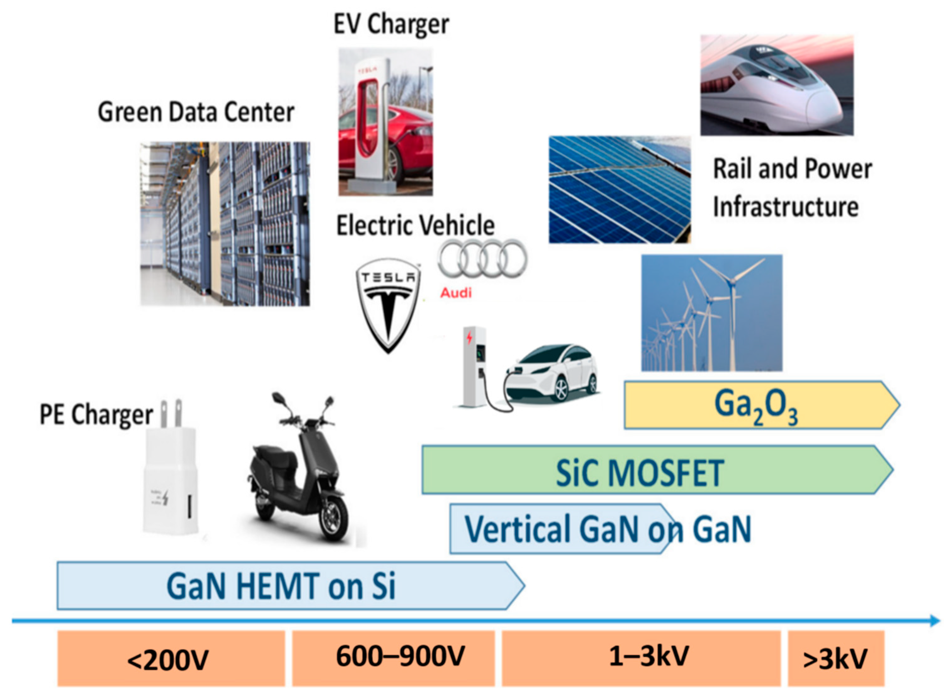
Figure 1. The distribution of wide bandgap power devices is based on voltage range.
2. GaN Power Devices
GaN-based power devices are primarily categorized into two fundamental structures: planar (lateral) structure devices and vertical structure devices, as depicted in Figure 2. Planar devices are typically manufactured on Si or SiC substrates, while vertical devices are homoepitaxially grown on GaN substrates. GaN HEMTs are the most commonly employed among GaN power devices. Si substrates are favored in their production to optimize cost-effectiveness and yield. However, epitaxially growing GaN on Si presents considerable challenges due to significant lattice mismatch and a substantial thermal expansion coefficient disparity between the two materials. The lattice mismatch can lead to dislocation propagation and defect generation throughout the GaN epitaxial layers, while thermal mismatch may cause cracking in the GaN layer during cooling after epitaxial growth [20,21,22][19][20][21]. To mitigate defect propagation and attain high-quality, defect-free GaN on Si, a meticulous optimization of the buffer region is imperative. Additionally, it is essential to limit tensile stress during both the growth and cooling phases of the process [23,24][22][23].
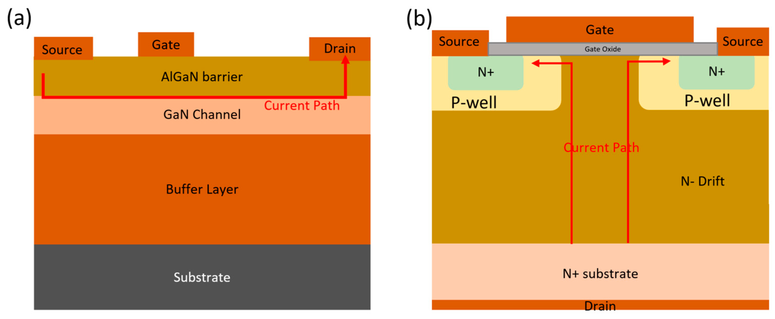
Figure 2. The schematic structures of (a) a lateral GaN device and (b) a vertical GaN device.
In addition to challenges related to epitaxial layer mismatch, the quality of the top surface becomes a critical concern for achieving optimal performance in lateral GaN devices. The presence of surface states on the AlGaN layer significantly influences the formation of the two-dimensional electron gas (2DEG) [25][24]. These states can have adverse effects on device performance by unintentionally depleting the 2DEG. This depletion can create a virtual gate between the gate and drain regions, leading to degradation in device performance and reliability. To counteract the depletion of the 2DEG, a well-optimized silicon nitride (SiN) passivation layer is typically employed.
Currently, commercially available GaN HEMTs offer a VBD of approximately 650/900V, coupled with a maximum output DC rating of 150A [26][25]. These devices find applications across various fields, including onboard battery chargers, high-efficiency power converters, and dense solar panel inverters. However, lateral GaN devices face specific limitations when it comes to scaling VBD and ensuring reliability. These limitations are primarily associated with lateral carrier flow from the source to the drain, with the electron density in the channel being highly sensitive to surface traps and buffer defects. Furthermore, these imperfections in the device can lead to phenomena such as current collapse and dynamic degradation of RON [26,27,28][25][26][27]. The severity of these adverse effects increases as VBD ratings rise. Moreover, the lateral electron transport nature results in a nonuniform distribution of the electric field within the device, leading to a higher electric field concentration in specific regions such as the gate, field plate, or drain edges. This nonuniform electric field distribution may result in premature semiconductor and dielectric breakdown, along with increased electron trapping at the surface. These factors contribute to performance degradation and limit the device’s voltage-blocking potential [28,29][27][28].
Furthermore, the VBD of lateral devices is directly proportional to the distance between the gate and drain, which increases both the device size and cost. Another significant concern with lateral GaN HEMT devices is that they are typically normally-ON devices. While various methods exist to create normally-OFF devices, such as using fluorine ion implantation [30,31[29][30][31],32], recess gates [33][32], p-GaN gates [34][33], trigate structures [35[34][35],36], cascode configurations [37[36][37],38], etc., the threshold voltage (VTH) achieved is typically around 1–2V in many cases, including commercial devices. This characteristic makes the device less than ideal for failsafe operation. Lastly, the absence of avalanche capability in lateral GaN devices, possibly due to the lack of a p–n junction between the drain and source regions, which aids in hole extraction during impact ionization, poses challenges in preventing the device from short-term overvoltage failure [39][38].
To address the limitations of lateral GaN devices, there has been a growing exploration and investigation of vertical GaN devices. The primary distinction between vertical and lateral devices lies in the direction of current flow, as illustrated in Figure 2 with a red arrow for both types. In a vertical device, current flows vertically from the bottom to the top surface (with electrons carrying the current from top to bottom) or in parallel with the direction of the GaN epitaxial layers. Consequently, current conduction occurs through the surface channel and then through a bulk drain drift region formed by a homoepitaxial GaN layer on a GaN substrate. Unlike lateral devices, vertical devices do not have a 2DEG drain drift region near the surface or a defect-rich buffer layer, as found in GaN HEMTs. As a result, there is less degradation in dynamic RON, which often occurs due to trapped impurity charges or bulk traps resulting from lattice mismatch [40][39]. One of the most significant advantages of vertical devices over lateral ones is their VBD. The VBD of a vertical device can be increased by augmenting the thickness of the N-drift layer, which is typically a low-doped or unintentionally doped GaN epitaxial layer (also known as the GaN N-drift layer). Consequently, this makes the VBD independent of the lateral size of the device. Moreover, a vertical GaN device can achieve a VTH ranging from around 5 to 15V, making it well-suited for high-power applications [41][40].
Another advantage of vertical GaN devices is their ability to exhibit avalanche breakdown, enhancing device reliability and potentially eliminating the need for overdesigning the device [42,43,44][41][42][43]. During transients, avalanche breakdown serves as a failsafe operation, allowing the device to operate closer to its material limits [45][44]. The VBD of a vertical GaN device can be significantly higher because the drain is located at the bottom of the device. When a high voltage is applied at the terminal, the electric field is evenly distributed throughout the device in a vertical direction, unlike lateral devices that experience electric field spikes at the gate edge [46][45]. This even distribution of the electric field within the device, away from the surface, can mitigate the effects of current collapse by countering the influence of surface states and thus slowing down the occurrence of current collapse [47,48][46][47]. Vertical GaN devices also offer the advantage of easily increasing power density. Since there are no electric field spikes, unlike lateral devices, there is no need for the field plate structure, which typically increases gate leakage spacing, to enhance breakdown performance. This makes it simpler to improve wafer utilization and boost power density [49][48].
The nFET operation of the vertical device is controlled by two primary p–n junctions, forming gate–source, and gate–drain diodes. Avalanche breakdown occurs when the drain–source voltage of the device exceeds its VBD. Initially, avalanche breakdown occurs through the reverse-biased drain–gate diode region, leading to an increase in the gate–source voltage and the opening of the channel region. Unlike lateral GaN devices, avalanche breakdown in vertical devices remains within the short-term power dissipation limits. Furthermore, energy dissipation occurs within the drift region of the device rather than on the surface (a sensitive region). This feature helps protect the device from transient spikes and other abnormal operating conditions. In a vertical GaN device, the epitaxial layer is grown homoepitaxially on the native GaN substrate, eliminating issues related to lattice or thermal expansion coefficient mismatches. The performance of the vertical GaN device remains unaffected by defect densities and manufacturing challenges such as wafer bow, warp, cracking, etc. Consequently, vertical GaN devices offer high reliability, yield, and, ultimately, reduced costs compared to lateral devices. Despite the significant potential of vertical GaN in dominating power devices, the current landscape still heavily relies on lateral device structures due to the complexities involved in preparing vertical devices and the high cost of GaN substrates [50][49].
A notable breakthrough in GaN devices is the introduction of GaN on SiC. GaN on SiC is a device that combines the advantages of both materials. The remarkable thermal conductivity of SiC, outperforming GaN alone, facilitates efficient heat dissipation, fostering enhanced device performance and durability. These devices are characterized by high power density and high-frequency response, attributes that lend themselves perfectly to applications in high-frequency electronics like radars and satellite communications. The symbiotic relationship between GaN and SiC, marked by minimal lattice mismatch and thermal stress, ensures devices that are reliable over extended operational timelines. This integration is known to reduce parasitic capacitances and resistances, paving the way for quicker device switching and diminished energy losses [51,52][50][51].
Despite the obvious advantages, SiC substrates tend to be more expensive compared to alternatives like Si or sapphire, which can escalate the overall device cost. The nuanced processes involved in the epitaxial growth of GaN on SiC lead to defects, which could compromise device efficiency. The demand for large-diameter SiC wafers often outstrips the supply, potentially hindering widespread commercial adoption and mass production [53,54][52][53]. A major issue with these devices is their compromised off-state performance, characterized by increased leakage and reduced VBD. Studies suggest that these defects can intensify leakage by acting as electron–hole pair generators under strong electric fields. As illustrated in some research, when exposed to high electric fields, these defects create holes that can accumulate at the boundary between the dielectric and the semiconductor. This accumulation can then intensify the field in the oxide, leading to a potential device failure. Interestingly, in comparisons using trench MOSFETs, devices on bulk GaN outperform those on alternative materials [55,56][54][55]. GaN on SiC in vertical devices is a tapestry of clear advantages punctuated by challenges.
References
- Chow, T.P.; Omura, I.; Higashiwaki, M.; Kawarada, H.; Pala, V. Smart Power Devices and ICs Using GaAs and Wide and Extreme Bandgap Semiconductors. IEEE Trans. Electron Devices 2017, 64, 856–873.
- Baliga, B.J. Trends in power semiconductor devices. IEEE Trans. Electron Devices 1996, 43, 1717–1731.
- Chow, T.P. Wide bandgap semiconductor power devices for energy efficient systems. In Proceedings of the 2015 IEEE 3rd Workshop on Wide Bandgap Power Devices and Applications (WiPDA), Blacksburg, VA, USA, 2–4 November 2015; pp. 402–405.
- Ding, X.; Zhou, Y.; Cheng, J. A review of gallium nitride power device and its applications in motor drive. CES Trans. Electr. Mach. Syst. 2019, 3, 54–64.
- Rodríguez, M.; Zhang, Y.; Maksimović, D. High-frequency PWM buck converters using GaN-on-SiC HEMTs. IEEE Trans. Power Electron. 2013, 29, 2462–2473.
- Meneghini, M.; De Santi, C.; Abid, I.; Buffolo, M.; Cioni, M.; Khadar, R.A.; Nela, L.; Zagni, N.; Chini, A.; Medjdoub, F. GaN-based power devices: Physics, reliability, and perspectives. J. Appl. Phys. 2021, 130, 181101.
- EPC2023—Enhancement Mode Power Transistor. Available online: https://epc-co.com/epc/Portals/0/epc/documents/datasheets/EPC2023_datasheet.pdf (accessed on 20 June 2023).
- EPC2012C—Enhancement Mode Power Transistor. Available online: https://epc-co.com/epc/Products/eGaNFETsandICs/EPC2012C.aspx (accessed on 20 June 2023).
- EPC2108—Enhancement-Mode GaN Power Transistor Half-Bridge with Integrated Synchronous Bootstrap. Available online: https://epc-co.com/epc/Portals/0/epc/documents/datasheets/EPC2108_datasheet.pdf (accessed on 20 June 2023).
- EPC launches 200V, 10mΩ GaN FET. Available online: https://www.semiconductor-today.com/news_items/2023/jan/epc-310123.shtml (accessed on 20 June 2023).
- TP65H480G4JSGB-650V SuperGaN® GaN FET in PQFN (source tab). Available online: https://www.transphormusa.com/en/document/datasheet-tp65h480g4jsgb-650v-gan-fet (accessed on 20 June 2023).
- TP65H050G4BS-650V SuperGaN® FET in TO-263 (source tab). Available online: https://www.transphormusa.com/en/document/datasheet-tp65h050g4bs-650v-gan-fet (accessed on 20 June 2023).
- 900V Cascode GaN FET in TO-247 (Source Tab). Available online: https://www.transphormusa.com/en/document/datasheet-tp90h050ws/ (accessed on 20 June 2023).
- Hwang, I.; Choi, H.; Lee, J.; Choi, H.S.; Kim, J.; Ha, J.; Um, C.Y.; Hwang, S.K.; Oh, J.; Kim, J.Y.; et al. 1.6kV, 2.9 mΩ cm2 normally-off p-GaN HEMT device. In Proceedings of the 2012 24th International Symposium on Power Semiconductor Devices and ICs, Bruges, Belgium, 3–7 June 2012; pp. 41–44.
- Dogmus, E.; Zegaoui, M.; Medjdoub, F. GaN-on-silicon high-electron-mobility transistor technology with ultra-low leakage up to 3000 V using local substrate removal and AlN ultra-wide bandgap. Appl. Phys. Express 2018, 11, 034102.
- Herbecq, N.; Roch-Jeune, I.; Linge, A.; Zegaoui, M.; Jeannin, P.-O.; Rouger, N.; Medjdoub, F. Above 2000 V breakdown voltage at 600 K GaN-on-silicon high electron mobility transistors. Phys. Status Solidi (A) 2016, 213, 873–877.
- Xiao, M.; Ma, Y.; Du, Z.; Pathirana, V.; Cheng, K.; Xie, A.; Beam, E.; Cao, Y.; Udrea, F.; Wang, H.; et al. Multi-Channel Monolithic-Cascode HEMT (MC2-HEMT): A New GaN Power Switch up to 10 kV. In Proceedings of the 2021 IEEE International Electron Devices Meeting (IEDM), San Francisco, CA, USA, 11–16 December 2021; pp. 5.5.1–5.5.4.
- Zhang, Y. Stretching GaN Power Devices to 10 kV. Available online: https://compoundsemiconductor.net/article/115524/Stretching_GaN_power_devices_to_10_kV (accessed on 20 June 2023).
- Zhou, S.Q.; Vantomme, A.; Zhang, B.S.; Yang, H.; Wu, M.F. Comparison of the properties of GaN grown on complex Si-based structures. Appl. Phys. Lett. 2005, 86, 081912.
- Dadgar, A.; Schulze, F.; Wienecke, M.; Gadanecz, A.; Bläsing, J.; Veit, P.; Hempel, T.; Diez, A.; Christen, J.; Krost, A. Epitaxy of GaN on silicon—Impact of symmetry and surface reconstruction. New J. Phys. 2007, 9, 389.
- Zhao, D.; Zhao, D. Analysis of the growth of GaN epitaxy on silicon. J. Semicond. 2018, 39, 033006.
- Wośko, M.; Szymański, T.; Paszkiewicz, B.; Pokryszka, P.; Paszkiewicz, R. MOVPE growth conditions optimization for AlGaN/GaN/Si heterostructures with SiN and LT-AlN interlayers designed for HEMT applications. J. Mater. Sci. Mater. Electron. 2019, 30, 4111–4116.
- Stanchu, H.V.; Kuchuk, A.V.; Mazur, Y.I.; Li, C.; Lytvyn, P.M.; Schmidbauer, M.; Maidaniuk, Y.; Benamara, M.; Ware, M.E.; Wang, Z.M. Local strain and crystalline defects in GaN/AlGaN/GaN (0001) heterostructures induced by compositionally graded AlGaN buried layers. Cryst. Growth Des. 2018, 19, 200–210.
- Ibbetson, J.P.; Fini, P.T.; Ness, K.D.; DenBaars, S.P.; Speck, J.S.; Mishra, U.K. Polarization effects, surface states, and the source of electrons in AlGaN/GaN heterostructure field effect transistors. Appl. Phys. Lett. 2000, 77, 250–252.
- del Alamo, J.A.; Joh, J. GaN HEMT reliability. Microelectron. Reliab. 2009, 49, 1200–1206.
- Ohki, T.; Kikkawa, T.; Inoue, Y.; Kanamura, M.; Okamoto, N.; Makiyama, K.; Imanishi, K.; Shigematsu, H.; Joshin, K.; Hara, N. Reliability of GaN HEMTs: Current status and future technology. In Proceedings of the 2009 IEEE International Reliability Physics Symposium, Montreal, QC, Canada, 26–30 April 2009; pp. 61–70.
- Saito, W. Reliability of GaN-HEMTs for high-voltage switching applications. In Proceedings of the 2011 International Reliability Physics Symposium, Monterey, CA, USA, 10–14 April 2011; pp. 4E.1.1–4E.1.5.
- Meneghesso, G.; Verzellesi, G.; Danesin, F.; Rampazzo, F.; Zanon, F.; Tazzoli, A.; Meneghini, M.; Zanoni, E. Reliability of GaN High-Electron-Mobility Transistors: State of the Art and Perspectives. IEEE Trans. Device Mater. Reliab. 2008, 8, 332–343.
- Chen, K.J.; Zhou, C. Enhancement-mode AlGaN/GaN HEMT and MIS-HEMT technology. Phys. Status Solidi (A) 2011, 208, 434–438.
- Chen, K.J.; Yuan, L.; Wang, M.J.; Chen, H.; Huang, S.; Zhou, Q.; Zhou, C.; Li, B.K.; Wang, J.N. Physics of fluorine plasma ion implantation for GaN normally-off HEMT technology. In Proceedings of the 2011 International Electron Devices Meeting, Washington, DC, USA, 5–7 December 2011; pp. 19.14.11–19.14.14.
- Yong, C.; Yugang, Z.; Chen, K.J.; Lau, K.M. High-performance enhancement-mode AlGaN/GaN HEMTs using fluoride-based plasma treatment. IEEE Electron Device Lett. 2005, 26, 435–437.
- Saito, W.; Takada, Y.; Kuraguchi, M.; Tsuda, K.; Omura, I. Recessed-gate structure approach toward normally off high-Voltage AlGaN/GaN HEMT for power electronics applications. IEEE Trans. Electron Devices 2006, 53, 356–362.
- Greco, G.; Iucolano, F.; Roccaforte, F. Review of technology for normally-off HEMTs with p-GaN gate. Mater. Sci. Semicond. Process. 2018, 78, 96–106.
- Ma, J.; Matioli, E. High Performance Tri-Gate GaN Power MOSHEMTs on Silicon Substrate. IEEE Electron Device Lett. 2017, 38, 367–370.
- Ma, J.; Matioli, E. Slanted tri-gates for high-voltage GaN power devices. IEEE Electron Device Lett. 2017, 38, 1305–1308.
- Zhang, W.; Xu, Z.; Zhang, Z.; Wang, F.; Tolbert, L.M.; Blalock, B.J. Evaluation of 600 V cascode GaN HEMT in device characterization and all-GaN-based LLC resonant converter. In Proceedings of the 2013 IEEE Energy Conversion Congress and Exposition, Denver, CO, USA, 15–19 September 2013; pp. 3571–3578.
- Huang, X.; Liu, Z.; Li, Q.; Lee, F.C. Evaluation and Application of 600 V GaN HEMT in Cascode Structure. IEEE Trans. Power Electron. 2014, 29, 2453–2461.
- Zhong, Y.; Zhang, J.; Wu, S.; Jia, L.; Yang, X.; Liu, Y.; Zhang, Y.; Sun, Q. A review on the GaN-on-Si power electronic devices. Fundam. Res. 2022, 2, 462–475.
- Nexgenpowersystems. Vertical GaN™ Theory of Operation. Available online: https://nexgenpowersystems.com/wp-content/uploads/2020/03/Theory_of_operation_TOC_r8.6.pdf (accessed on 1 July 2023).
- Oka, T.; Ueno, Y.; Ina, T.; Hasegawa, K. Vertical GaN-based trench metal oxide semiconductor field-effect transistors on a free-standing GaN substrate with blocking voltage of 1.6 kV. Appl. Phys. Express 2014, 7, 021002.
- Kizilyalli, I.C.; Edwards, A.P.; Nie, H.; Disney, D.; Bour, D. High Voltage Vertical GaN p-n Diodes with Avalanche Capability. IEEE Trans. Electron Devices 2013, 60, 3067–3070.
- Santi, C.D.; Fabris, E.; Meneghesso, G.; Zanoni, E.; Meneghini, M. GaN Vertical p–i–n Diodes in Avalanche Regime: Time-Dependent Behavior and Degradation. IEEE Electron Device Lett. 2020, 41, 1300–1303.
- Maeda, T.; Narita, T.; Ueda, H.; Kanechika, M.; Uesugi, T.; Kachi, T.; Kimoto, T.; Horita, M.; Suda, J. Design and Fabrication of GaN p-n Junction Diodes with Negative Beveled-Mesa Termination. IEEE Electron Device Lett. 2019, 40, 941–944.
- Oka, T. Recent development of vertical GaN power devices. Jpn. J. Appl. Phys. 2019, 58, SB0805.
- Sochacki, T.; Bryan, Z.; Amilusik, M.; Bobea, M.; Fijalkowski, M.; Bryan, I.; Lucznik, B.; Collazo, R.; Weyher, J.L.; Kucharski, R.; et al. HVPE-GaN grown on MOCVD-GaN/sapphire template and ammonothermal GaN seeds: Comparison of structural, optical, and electrical properties. J. Cryst. Growth 2014, 394, 55–60.
- Mizutani, T.; Ohno, Y.; Akita, M.; Kishimoto, S.; Maezawa, K. A study on current collapse in AlGaN/GaN HEMTs induced by bias stress. Electron Devices IEEE Trans. 2003, 50, 2015–2020.
- Yu, C.; Luo, X.D.; Zhou, W.; Luo, Q.Z.; Liu, P.s. Investigation on the current collapse effect of AlGaN/GaN/InGaN/GaN doubleheterojunction HEMTs. Wuli Xuebao/Acta Phys. Sin. 2012, 61, 207301.
- Yaegassi, S.; Okada, M.; Saitou, Y.; Yokoyama, M.; Nakata, K.; Katayama, K.; Ueno, M.; Kiyama, M.; Katsuyama, T.; Nakamura, T. Vertical heterojunction field-effect transistors utilizing re-grown AlGaN/GaN two-dimensional electron gas channels on GaN substrates. Phys. Status Solidi (C) 2011, 8, 450–452.
- Chen, K.J.; Häberlen, O.; Lidow, A.; Tsai, C.l.; Ueda, T.; Uemoto, Y.; Wu, Y. GaN-on-Si Power Technology: Devices and Applications. IEEE Trans. Electron Devices 2017, 64, 779–795.
- Li, Y.; Yang, S.; Liu, K.; Cheng, K.; Sheng, K.; Shen, B. Low ON-Resistance Fully-Vertical GaN-on-SiC Schottky Barrier Diode with Conductive Buffer Layer. In Proceedings of the 2022 IEEE 34th International Symposium on Power Semiconductor Devices and ICs (ISPSD), Vancouver, BC, Canada, 22–25 May 2022; pp. 333–336.
- Li, Y.; Yang, S.; Liu, K.; Cheng, K.; Sheng, K.; Shen, B. Fully-Vertical GaN-on-SiC Schottky Barrier Diode: Role of Conductive Buffer Structure. IEEE Trans. Electron Devices 2023, 70, 619–626.
- Liu, J.; Xiao, M.; Zhang, R.; Pidaparthi, S.; Cui, H.; Edwards, A.; Craven, M.; Baubutr, L.; Drowley, C.; Zhang, Y. 1.2-kV Vertical GaN Fin-JFETs: High-Temperature Characteristics and Avalanche Capability. IEEE Trans. Electron Devices 2021, 68, 2025–2032.
- Liu, J.; Zhang, R.; Xiao, M.; Pidaparthi, S.; Cui, H.; Edwards, A.; Baubutr, L.; Drowley, C.; Zhang, Y. Surge Current and Avalanche Ruggedness of 1.2-kV Vertical GaN p-n Diodes. IEEE Trans. Power Electron. 2021, 36, 10959–10964.
- Zhang, Y.; Dadgar, A.; Palacios, T. Gallium nitride vertical power devices on foreign substrates: A review and outlook. J. Phys. D Appl. Phys. 2018, 51, 273001.
- Khadar, R.A.; Liu, C.; Zhang, L.; Xiang, P.; Cheng, K.; Matioli, E. 820-V GaN-on-Si Quasi-Vertical p-i-n Diodes with BFOM of 2.0 GW/cm2. IEEE Electron Device Lett. 2018, 39, 401–404.
More