Your browser does not fully support modern features. Please upgrade for a smoother experience.
Please note this is a comparison between Version 1 by Lin-Qing Zhang and Version 2 by Lindsay Dong.
β-Ga2O3, with excellent bandgap, breakdown field, and thermal stability properties, is considered to be one of the most promising candidates for power devices including field-effect transistors (FETs) and for other applications such as Schottky barrier diodes (SBDs) and solar-blind ultraviolet photodetectors. Ohmic contact is one of the key steps in the β-Ga2O3 device fabrication process for power applications.
- β-Ga2O3
- Ohmic contact
- ion implantation
- interface
1. Introduction
Si-based devices are the dominant devices used for power applications. However, with the increasing demand for much faster and more convenient network communication, Si-based device techniques cannot meet these requirements due to their physical properties. Thus, new-material devices should be investigated for operating at high temperatures, at high power, and in harsh environments. In recent years, wide-bandgap semiconductors including GaN (3.4 eV) and SiC (3.25 eV) have been developed, and they have replaced Si-based techniques in many fields due to their advantages in terms of their material properties [1][2][3][4][5][1,2,3,4,5]. Recently, β-Ga2O3, which is mostly thermally and chemically stable in five polymorphs [6][7][8][6,7,8], has attracted more and more attention for power applications because β-Ga2O3 has a wide bandgap of 4.6–4.9 eV and a breakdown field strength as high as 8 MV/cm [9][10][11][9,10,11]. In addition, for the Baliga figure and Johnson’s figure of merit, when evaluating its application potential in power devices, β-Ga2O3 exhibits the best performance [9][10][11][9,10,11].
where χ represents the semiconductor’s electron affinity (4 eV for Ga2O3 in thecase [15][60]) and Φm represents the metal work function. Therefore, it is desirable to select a metal with a Φm lower than 4 eV to realize a negative ΦB, which allows electrons to flow freely across it to form an Ohmic contact. Unfortunately, the lack of suitable metal materials with lower work functions makes Ohmic contact formation challenging. Generally, researchers have proposed Ohmic contact schemes to form a lower ΦB or an n+-doped Ga2O3 region for electron tunneling. When a semiconductor is heavily doped (ND > 1018 cm−3), field emission (FE) dominates the electron tunneling [16][17][61,62]. In order to obtain a low RC or ρc, a higher ND is expected.
2. Basic Metal–Ga2O3 Contact Physical Theory
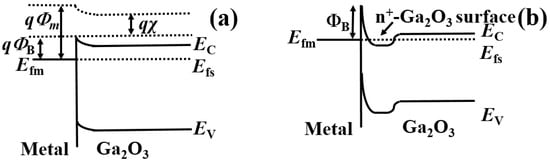
Metal–semiconductor contact is a critical part of β-Ga2O3 power devices. A device’s performance is mainly limited by the Ohmic contact property. Two types of contacts (Schottky and Ohmic) can be formed due to the differences in the work functions of contact metals [12][13][14][57,58,59]. For wide-bandgap β-Ga2O3, the contacts always exhibit Schottky behavior. When metal and Ga2O3 come into contact, the energy band of the Ga2O3 side bends up to make their Fermi levels equal. As shown in Figure 1a, the Schottky barrier height from the metal side (ΦB) can be described asΦB
=
Φm
−
χ,
,
Figure 1.
Energy-band diagrams of metal–Ga
2
O
3
Schottky contacts with (
a
) a lower
Φbn
and (
b
) an n
+
-doped Ga
2
O
3
region.
The Ohmic contact resistance (RC, measured in Ω·mm) and specific contact resistance (ρc, measured in Ω·cm−2) are always determined using the transmission line model (TLM) method [18][19][63,64]. Details concerning the TLM measurement technique can be seen in the references mentioned above.
The metal work function, metal schemes, interfacial reactions between metal and a semiconductor during the annealing process, and the doping concentration of Ga2O3 in the source/drain region are significant influencing factors for the Ohmic contact property. Until now, researchers from universities and research institutes have proposed Ohmic contact schemes involving optimizing the metal materials, annealing condition, source/drain doping method and concentration, and source/drain etching as well as adding an interlayer in the source/drain region.
3. Approaches to Metal–Ga2O3 Ohmic Contact
3.1. Metal Electrode
From the metal–semiconductor contact theory, the work function of the selected metal material crucially affects the Ohmic contact quality. Thus, in the early period, Yao et al. [20][65] investigated the Ohmic contact properties and surface morphologies of nine metal materials, including Ti, In, Ag, Sn, W, Mo, Sc, Zn, and Zr with Sn-doped (2̲ 01) β-Ga2O3. From their results, the work function is not the main factor influencing the contact quality. Sc, with the lowest work function, cannot form Ohmic contacts under different annealing conditions. Ti/Au metal schemes with a 400 °C annealing process exhibited the lowest RC values. Cross-sectional transmission electron microscopy (TEM) and energy-dispersive X-ray spectroscopy (EDX) mapping showed that Ga and O diffused into the Ti layer during the annealing process. They concluded that interfacial reactions during the annealing process played a crucial part in Ohmic contact formation.
Other groups have reported Mg/Au and Cr/Au metal schemes for Ohmic contact formation [21][22][66,67]. In the Mg (3.66 eV)/Au method, the ρc of 2.2 × 10⁻⁴~2.1 × 10⁻⁵ Ω·cm−2 was achieved with an annealing process at temperatures varying from 300 °C to 500 °C. Until now, the most common metallization schemes of Ohmic contact for β-Ga2O3 have used Ti/Au. Ti is used as an adhesion layer with a low work function. Au serves as a cap layer to prevent the oxidation of metal stacks during the high-temperature process.
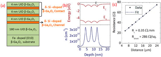
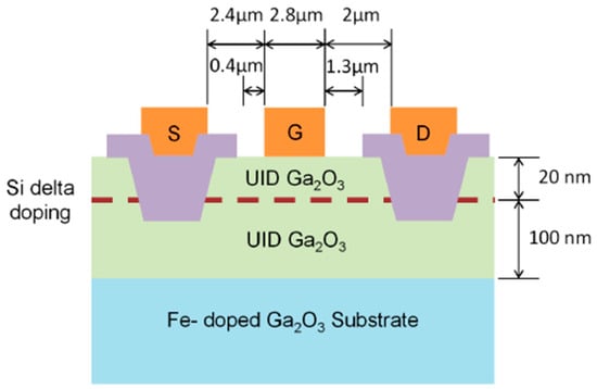
Also, multilayer metal contact schemes were proposed for obtaining lower RC values, such as Ti/Al/Au [23][24][70,71], Ti/Al/Ni/Au [25][26][72,73], and Ti/Au/Ni [27][28][32,33]. As can be seen in Figure 23, Krishnamoorthy et al. formed a δ-doped β-Ga2O3 structure in the source/drain region to form a heavily doped contact area. After Ti/Au/Ni deposition, a 470 °C RTA process was employed for 1 min for Ohmic contact formation. The extracted RC and ρc were 0.35 Ω·mm and 4.3 × 10⁻⁶ Ω·cm−2, respectively. In addition, the fabricated β-Ga2O3 FET exhibited excellent ID and gm results. By using Ti/Al/Au contact metals, Zhou et al. [24][71] achieved a low RC of 0.75 Ω·mm by adopting a highly Sn-doped channel.
Figure 23.
(a
) Device structure, (b
) equilibrium band diagram and charge profile, and () TLM results. Reproduced from Ref. [33].
In 2022, Tetzner et al. [29][76] used a TiW alloy instead of the traditional Ti/Au metal schemes, and a low ρc of 1.5 × 10⁻⁵ Ω·cm−2 was extracted after a 700 °C RTA process. The temperature was 200 °C higher than that of the Ti/Au schemes. To understand the Ohmic contact formation mechanism, STEM HAADF and EDX were employed. The STEM HAADF image showed that a 3–5 nm TiOX interlayer was formed, which was confirmed with the STEM EDX. They suspected that vacancies, defects, or Ga impurities that exist in the interlayer are beneficial for electrons flowing freely to reduce the RC.
Thermal stability is another important index of contact quality. For Ti/Au electrodes, the most commonly used annealing temperatures are between 400 °C to 500 °C. Above 500 °C, Yao et al. [20][65] found that the Ohmic contacts degraded in their results. In 2022, Lee et al. [30][77] systematically investigated the influence of temperature on Ohmic contact quality. In their results, when the annealing temperature increased from 470 °C to 520 °C, aggressive Au diffused into the interface and reacted with Ga that diffused out, resulting in a much thicker Ti–TiOx layer due to GaAu2 formation, which accounted for the contact degradation.
3.2. Surface Treatment
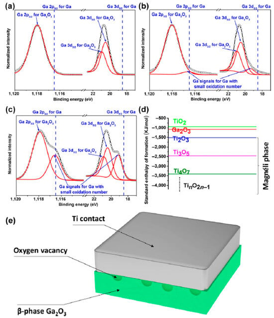
A surface treatment before metal deposition can also help improve the Ohmic contact property (dry etching, plasma bombardment, etc.). In 2012, Higashiwaki et al. [31][82] compared the I–V results of Ga2O3 devices with and without the RIE treatment. The RIE process was implemented by using a BCl3/Ar mixing gas for 1 min before Ti/Au (20/230 nm) deposition. The samples with the RIE treatment exhibited Ohmic contact characteristics, while without the RIE process the samples showed Schottky contact features. They speculated that the Ohmic contact formation was due to the large number of oxygen-vacancy surface defects formed during the RIE process. The defects acted as donors for Ohmic contact realization. Combined with Si ion implantation [32][83], they achieved a ρc of 4.6 × 10⁻⁶ Ω·cm−2 with a doping concentration of 5 × 1019 cm−3. Also, the annealing temperature and atmosphere may affect the interfacial reactions that dominate Ohmic contact formation. Bae et al. [33][87] compared the electrical results of the fabricated β-Ga2O3 nanobelts under different atmospheres with various temperatures. The samples treated under a N2 atmosphere exhibited better characteristics that the ones treated in an air environment. Under an Ar atmosphere, Li et al. [34][88] reduced the RC to 0.387 Ω·mm by optimizing the annealing temperature and the durations. In their results, a large drain current density of ~3.1 mA/μm (Vds = 100 V) was achieved due to the low RC. To fully understand the influence of an Ar atmosphere on improving the β-Ga2O3 device’s I–V characteristics, XPS was used to show the material changes during the RTA process. From the results, as can be seen in Figure 335, they deduced that Ti reduced β-Ga2O3 and generated large numbers of oxygen vacancies at the interface during the annealing process, which served as effective electron donors. For this reason, the depletion layer was narrower, resulting in Ohmic behavior and a low RC for β-Ga2O3 FETs. The annealing temperature is another element that affects the interface reactions to determine the Ohmic contact property.Figure 35. XPS results from β-Ga2O3. (a) Normalized Ga 2p3/2 XPS spectra and Ga 3d XPS spectra from pure β-Ga2O3, (b) β-Ga2O3 after annealing in argon at 300 °C for 180 min, and (c) Ti-coated (1 nm) β-Ga2O3 after annealing in argon at 300 °C for 180 min. Black dots show experimental data, and red curves show simulated fitting curves. (d) Free energy scheme of different metal oxides. (e) Schematic diagram of the proposed oxygen vacancy model at the Ti/β-Ga2O3 interface. Reproduced from Ref. [34][88].
3.3. Ion Implantation
The ion-implantation doping technique (including Si, Sn, etc.) is another effective way for Ga2O3 to realize low-contact-resistance Ohmic electrodes by forming a heavily doped n+ region that facilitates electron flow. In 2013, Sasaki et al. [32][83] successfully fabricated Ohmic electrodes with a low contact resistance via Si implantation, which requires the MOVPE method in β-Ga2O3. They optimized the Si doping concentration to 5 × 1019 cm−3, which was activated by annealing at a temperature of 950 °C. The RC and ρc in their results were as low as 1.4 mΩ·cm and 4.6 × 10⁻⁶ Ω·cm−2, respectively. In other results, Zhou et al. [23][70] doped β-Ga2O3 with Sn at a concentration of 2.7 × 1018 cm−3. Combined with Ar plasma bombardment, the RC was dramatically reduced to 0.95 Ω·mm. The fabricated devices also exhibited an excellent on/off ratio and output characteristics and a low SS value. In addition, Ge and Sn were also studied for doping β-Ga2O3 [35][89]. In that study, the samples were treated under the same annealing condition (925 °C for 30 min). The efficiencies of Sn, Ge, and Si were calculated to be 28.2%, 40.3%, and 64.7%, respectively, using SIMS measurements. The same activation annealing condition for Ge and Sn with Si resulted in low activation efficiencies for Ge and Sn. The heavier Ge and Sn ions also created more implant damage than the Si ions due to the greater momentum transfer required to achieve the same implant depth, likely contributing to decreased implant activation and increasing both the contact and sheet resistances.
3.4. Epitaxial Regrowth
To further reduce the contact resistance, regrown contacts have been reported to fabricate Ohmic contacts. Ion implantation and spin-on-glass techniques need a high annealing temperature around 900–1200 °C and potentially deteriorate the material quality in the active region. However, the regrowth process, which is performed at a much lower temperature of about 600 °C can avoid this potential problem. In 2018, Xia et al. [27][32] used a molecular-beam epitaxy (MBE) method to form a heavily doped n-type Ga2O3 with a doping concentration of 2 × 1020 cm−3. The device’s structure can be seen in Figure 48. An extracted RC of 1.5 Ω·mm was obtained from the TLM structure. The regrowth technique avoids gate recessing and potential damage associated with etching, which may degrade the carrier mobility. The fabricated devices exhibited a peak drain current of 140 mA/mm and an excellent transconductance of 34 mS/mm.Figure 48.
Device schematic of delta-doped β-Ga
2
O
MESFET. Reproduced from Ref. [32].
The existing results that have been reported in recent years demonstrate that regrown contact is an effective approach to achieve an ultralow RC. Epitaxial regrowth obtains a high-quality crystalline film and can be versatile. However, there are also several constraints, such as low throughput, high expense, strict material compatibility, and the need for selective growth or subsequent etchings, as mentioned in Refs. [36][37][97,98].
3.5. Adding the Interlayer
The Ti/Au schemes always form a 3–5 nm interlayer, which facilitates electron transport for Ohmic contact formation. Another approach is inserting an intermediate semiconductor layer (ISL) with a low work function and a narrower bandgap. In 2016, Oshima et al. [38][99] proved the insertion of indium tin oxide (ITO) for forming Ohmic contact with β-Ga2O3. In their results, as shown in Figure 510, the ITO method exhibited Ohmic behavior at temperatures from 900 °C to 1150 °C. However, Pt/β-Ga2O3 maintained Schottky contact, even at the RTA temperature of 500 °C. They also confirmed the existence of an intermediate semiconductor layer (ISL) at the interface using TEM and EDS analyses.
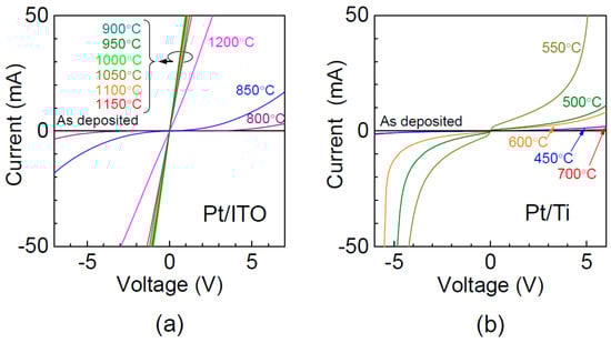
Figure 510.
Typical I–V characteristics of (
a
) Pt/ITO and (
) Pt/Ti electrodes annealed at various temperatures. Reproduced from Ref. [99].
Other elements such as substrate orientation have also been reported to influence the Ohmic contact property. To form Ohmic contact, Ti/Au contacts were deposited, followed by an RTA process at 450 °C for 5 min, which was employed on both (2̲
01) and (010) Sn-doped Ga2O3. The former sample exhibited Ohmic characteristics compared to the rectifying behavior of the (010) sample. Related content has also been investigated and reported by other groups [39][40][41][42][106,107,108,109].
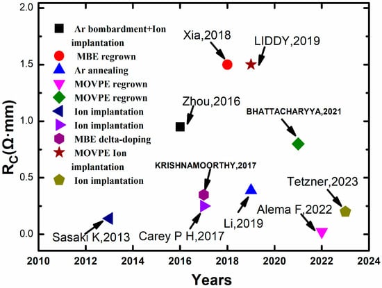
In recent years, researchers have investigated and optimized the Ohmic contact property of β-Ga2O3 by choosing a metal with a proper work function and investigating metal schemes, interfacial reactions between metal and semiconductors during the annealing process, and the doping concentration of Ga2O3 in the source/drain region, and they have achieved excellent results. Representative results with excellent Ohmic contact quality are summarized in Figure 615 [23][27][28][32][34][43][44][45][46][47][32,33,36,37,70,83,88,90,96,100]. Despite the significant improvement in the Ohmic contact techniques for β-Ga2O3, there are also some questions that need to be solved before commercializing the devices. (1) For power device applications, contact performance in high-temperature, -current, and -voltage environments is another concern. Failure analyses of the electrical stress/cycling of Ohmic electrodes have been investigated for other WBG semiconductor systems [48][49][50][110,111,112], while for β-Ga2O3, the research is lacking and efforts should be made to understand the degradation mechanism of Ohmic contacts under electrical stress. (2) To realize the integration of β-Ga2O3 semiconductors into Si CMOS technology, Au-free metal schemes should be investigated and proposed. The commonly used Ti/Au layer for Ga2O3 is not CMOS-compatible due to the existence of Au, which is a contaminant for Si fabrication lines [51][52][113,114]. Au is used for oxidation protection. Some oxidation-resistant capping materials, such as TiN, which has been proven to realize low-RC Ohmic contact in AlGaN/GaN HEMT [53], can be substitutes for Ohmic contact realization in β-Ga2O3 devices. Related investigations should be carried out to prove the feasibility of Au-free schemes. (3) RIE, ion implantation, and epitaxial regrowth are used to achieve a low RC. For the RIE process, the influences of plasma gas (including BCl3/Ar, Ar, and CF4 [54][115]), plasma power, bias power, etc., should be fully understood. For ion implantation, the high-temperature annealing used for impurity activation and damage recovery may cause unwanted effects, which should be noticed and further studied. In addition, the effect of substrate orientation should also be investigated. Other annealing techniques can also be used for Ohmic contact formation in β-Ga2O3 devices [55][56][116,117].