Epidermal electronics, an emerging interdisciplinary field, is advancing the development of flexible devices that can seamlessly integrate with the skin. These devices, especially Electric Double Layer (EDL)-based sensors, overcome the limitations of conventional electronic devices, offering high sensitivity, rapid response, and excellent stability. Especially, Electric Double Layer (EDL)-based epidermal sensors show great potential in the application of wearable electronics to detect biological signals due to their high sensitivity, fast response, and excellent stability. The advantages can be attributed to the biocompatibility of the materials, the flexibility of the devices, and the large capacitance due to the EDL effect.
- epidermal electronics
- electric double layer
- healthcare
1. Introduction
2. Material Synthesis
In the field of electrochemistry, the Electric Double Layer (EDL) stands out as a molecularly thin interface separating two substances populated by electrically charged particles. These can include an electrode from a solid material and an electrolyte solution [15][29]. Constituted of two layers of opposite charges, the EDL is structured by the adsorption of ions on the solid surface, thereby forming one layer. Concurrently, the other layer forms within the proximate solution near the surface. Owing to the separation between these charges, the EDL possesses a remarkably high capacitance. Consequently, the EDL holds a pivotal role in affecting various physical and chemical processes unfolding at the interface. Owning to the advantages of EDL, an EDL electrode emerges as an electrode to store electric charge at the electrolyte solution interface [16][30]. By their high charge density and rapid charge-discharge rates, EDLs are attractive in applications, such as electrochemical capacitors, sensors, and actuators. However, it is imperative to note that the performance relies on the factors, such as electrode material and electrolyte composition [17][31] as presented in Table 1.| Material | Electrical Conductivity (S/m) | Mechanical Strength (MPa) | Reference |
|---|---|---|---|
| Gold | 4.1 × 10⁷ | 120 | [18][34] |
| Silver | 6.3 × 10⁷ | 250 | [18][34] |
| Copper | 5.8 × 10⁶ | 210 | [18][34] |
| Polyimide | 1 × 10⁻¹⁴ | 50–170 | [19][35] |
| PDMS | 8130 | 1–5 | [19][35] |
| PET | 1 × 10⁻¹⁴ | 50–80 | [19][35] |
| Polyaniline | 5 | 20–100 | [20][36] |
| Polypyrrole | 40–200 | 30–80 | [20][36] |
| PEDOT | 300–1000 | 10–20 | [20][36] |
| Galinstan | 3.46 × 10⁶ | N/A | [21][37] |
| Silver Nanowire | 1 × 10⁴–8 × 10⁵ | 10–100 | [22][38] |
| Collagen | 10−6–10−4 | 0.1–1 | [23][39] |
| Chitosan | 10−5–10−4 | 1–5 | [23][39] |
| Hyaluronic Acid | ~10−3 | 0.05–0.5 | [23][39] |
| PCL (Poly-caprolactone) | 2.1 × 10⁻¹⁴ | 5–50 | [24][40] |
| PLA (Polylactic acid) | 10−15–10−13 | 40–60 | [24][40] |
2.1. Metal Based Materials
Galinstan [25][41] and silver nanowires (AgNW) [26][42] are typical representatives of metal-based materials and have emerged as prominent options offering flexibility [27][43], transparency [28][44], and biocompatibility for the devices. These materials present innovative solutions for biomedicine, wearable devices, and other related applications. In addition, a number of researches have been carried out to further enhance the material properties, such as the development of self-healing [29][45], shape-memory [30][46], and stimuli-responsive materials [31][47]. The use of liquid metals, such as Magnetic Liquid Metal (Fe-EGaIn) and Galinstan, enables exceptional stretchability and electrical conductivity of the devices, which are able to overcome the limitations of traditional solid metals. Nanowires, as another representative of metal-based materials, have also shown great potential in the development of flexible, transparent, and biocompatible devices due to their excellent electrical and mechanical properties [32][49]. Among the various nanowires, AgNW is a notable example of nanowires that possess excellent electrical and mechanical properties while maintaining flexibility, transparency, and biocompatibility [33][50]. Therefore, it has been widely employed in the fabrication of transparent conductive films for flexible and wearable electronics [34][35][51,52].2.2. Polymer-Based Materials
Recently, polymeric materials, such as polyimide (PI) [36][54], polydimethylsiloxane (PDMS) [37][55], and polyethylene terephthalate (PET) [38][56], which provide lightweight, highly flexible, and processable alternative properties, were also employed to be used as substrates and functional layers. In 2011, Kim et al. demonstrated the feasibility of using polyimide as a substrate for the fabrication of stretchable and flexible electronic devices [39][57]. They successfully fabricated a transparent and stretchable conductor using a combination of graphene and a polyimide substrate. The device exhibited excellent mechanical and electrical properties, highlighting the potential of polymeric materials in the application of flexible electronics. Their innovation in integrating thin-film transistors, temperature sensors, and strain gauges on a polyimide substrate shows the potential of the fabrication of micro and nanodevices with polymeric materials. With the employment of polymeric materials and various fabrication technologies, researchers enhanced device performance by optimizing the properties and functionality of these materials, which led to a substantial leap in the functionality and versatility of the devices. While polymeric materials have been widely employed in flexible electronics, their low electrical conductivity poses a challenge to further enhance the device’s performance. To overcome this issue, conductive polymers such as polyaniline [40][59], polypyrrole [41][60], and poly(3,4-ethylenedioxythiophene) (PEDOT) [42][61] were developed. In addition, through doping these conductive polymers with other materials like carbon nanotubes, graphene, and metallic nanoparticles, researchers were able to further enhance their electrical conductivity. To better understand the working mechanism of the EDL effect in these materials, it is important to develop theoretical and experimental methods that can capture the microscopic structure of the electrochemical interface and its working mechanisms. However, modeling and measuring the EDL structure for complex systems involving conductive polymers and their hybrid materials remains a challenge. For example, the effects of polymer chain conformation, molecular interactions, and ion solvation on EDL behavior are not fully understood.2.3. Bioinspired-Materials
Biomaterials have become more attractive for the application of epidermal electronics due to their high biocompatibility and degradability. Researchers have employed biomaterials to develop highly biocompatible, biodegradable flexible sensors, stimulators, drug delivery devices, and artificial neural networks [39][43][44][57,66,67]. Materials like silk fibroin, chitosan, and cellulose, which show potential for long-term stability and conformability with the human body [45][46][47][68,69,70], have been extensively investigated for their application in flexible devices. Also, hydrogel, a highly hydrated network of polymers, has been employed to develop sensors and actuators since it is able to closely mimic the properties of biological tissues [48][71]. The exploration of EDL phenomena in various material systems has significantly contributed to the development of next-generation electronic devices, especially for epidermal electronics. These advancements in material synthesis have been addressing some challenges in this field, such as the long-term stability of devices, signal processing and data transmission efficiency, and improving wearing comfort [49][50][77,78].3. Device Fabrication
3.1. Subtractive Manufacturing
Subtractive manufacturing enables precise patterning of the materials and is considered a crucial technique in the fabrication of epidermal electronic devices. As researchers strive to optimize the fabrication process, it is essential to consider the unique requirements of each device. Factors such as resolution, throughput, and processing compatibility are usually taken into consideration. While each technique has its advantages and drawbacks, advancements in subtractive manufacturing, along with the development of novel hybrid and additive processes, will contribute to the development of epidermal electronic devices by enhancing their performance, functionality, and conformability with the human body. Lithography is a versatile manufacturing technique that utilizes light to pattern the thin film. As a result, a desired shape or structure can be defined. This technique is widely used in epidermal electronics, where lithography can be applied to produce thin, flexible, and conformable devices with microstructures to monitor various physiological signals. Laser cutting is a technique that uses a high-power laser beam to cut materials into desired patterns, with advantages in fast speed, low cost, and high accuracy. This method can also be applied to fabricate epidermal electronics that can conform to the skin and have sensing, heating, and communication functions.3.2. Additive Manufacturing
Inkjet printing is another method for the fabrication of epidermal electronics, enabling the precise deposition of conductive, semi-conductive, or insulating materials onto a flexible substrate. This technique uses inkjet printer nozzles to accurately eject ink droplets, forming a patterned circuit on the substrate. Despite its high resolution, cost-effectiveness, and scalability, inkjet printing faces challenges such as ink dispersion and film formation, which can hinder the creation of uniform and well-controlled layers. Screen printing This technique is able to transfer material with a designed pattern onto a stretchable and flexible substrate using a stencil or mesh screen. In brief, the substrate is covered with the screen, which is then used to squeegee the ink through the mesh openings and onto the substrate, a circuit with the desired pattern can be realized. Three-dimensional (3D) printing This method can be used to fabricate three-dimensional devices layer by layer, enabling the fabrication of biocompatible electrodes and wearable electronics with complex structures. One of the 3D printing processes is Stereolithography (SLA), which converts liquid resin into solid layers by curing it with a laser, creating models, prototypes, patterns, and production parts [51][93]. Other 3D printing processes include fused deposition molding (FDM), and selective laser sintering (SLS), which have been used for epidermal electronics [52][94]. However, 3D printing is a relatively low efficiency and low resolution additive manufacturing technique. Recently, advances in multi-material and high-resolution printing have been investigated to overcome these limitations [53][54][95,96]. 3D printing is a promising technique for creating customized flexible devices that can conform to the skin’s surface and adapt to its deformation. Aerosol jet printing is an innovative technique that employs a carrier gas to deposit a fine mist of material onto a substrate, which is then cured using a laser or other methods. This method has the advantages of high resolution, low-temperature processing, and direct writing on various substrates, and it is widely employed in the fabrication of epidermal electronics. Jing et al. demonstrated a novel approach to the fabrication of freestanding functional structures layer by layer with aerosol jet printing [55][97]. Transfer printing is a sophisticated technology that integrates additive and subtractive manufacturing techniques to enable the precise and efficient fabrication of flexible devices [56][100], such as stretchable strain sensors [57][101], radio frequency (RF) power harvesters [58][102], and transistors [59][103].4. Integration Techniques for Rigid and Flexible Components
4.1. Interconnects for the 2D and 3D Dimensions
Interconnects serve as a critical component within the architecture of epidermal electronic devices, facilitating essential electrical connections among various components [60][61][62][104,105,106]. Numerous strategies exist for the realization of 2D and 3D interconnects, with printing emerging as a prevalent method [63][107]. To accommodate strain and bending, these interconnections can adopt an array of geometries, such as serpentine, helical, or buckled shapes.4.2. Rigid IC Chip Bonding to Soft Substrates
This procedure entails the utilization of adhesives, solder, or other bonding agents to secure rigid chips onto flexible substrates [64][65][66][108,109,110]. The objective is to establish robust electrical contact, mechanical stability, and thermal compatibility. The choice of an appropriate bonding technique is pivotal to the success of this process. A variety of bonding methods are frequently employed, each presenting its own unique advantages and considerations.4.3. Anisotropic Conductive Film (ACF) Bonding
ACF, a composite material composed of conductive particles and adhesive, serves a dual function: it provides mechanical adhesion and establishes an electrical connection between the rigid chip and the flexible substrate [67][68][69][111,112,113].4.4. Epoxy-Based Bonding
Epoxy adhesives, known for their superior adhesion to a wide range of materials and high mechanical strength, are considered suitable candidates for bonding rigid chips to flexible substrates [65][70][109,114]. Depending on the specific requirements of the device, conductive epoxies or different interconnects, such as wire bonding or flip-chip methods, can be employed to achieve the electrical connection.5. Applications of Epidermal Electronics in Diagnosis and Therapeutics
5.1. Diagnostic Applications of Epidermal Electronics
5.1.1. Mechanical Signal Monitoring
Epidermal Dielectric Layer (EDL) capacitive sensors exhibit remarkable sensitivity, a large span, and a short response time, making them an ideal solution for epidermal electronics [71][72][117,118]. These sensors have the ability to detect force and human muscle movement and adhere to human skin, thereby providing a versatile platform for various diagnostic applications in healthcare. Figure 10 shows different applications based on electrically double-layered epidermal electronics.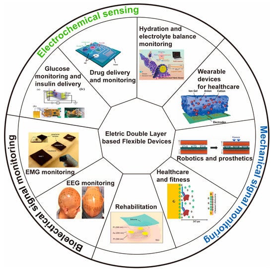
5.1.2. Bioelectrical Signal Monitoring
5.2. Therapeutic Applications of Epidermal Electronics
5.2.1. Therapeutic Applications in Robotics and Prosthetics
EDL pressure sensors can be amalgamated into robotic and prosthetic limbs to furnish precise tactile feedback and control, thereby aiding therapy and the rehabilitation process. Xu et al. [90][142] developed a stretchable and anti-impact iontronic pressure sensor featuring an ultra-broad linear range for biophysical monitoring and deep learning-aided knee rehabilitation. The sensor can track biophysical signals like pulse waves, muscle movements, and plantar pressure, while accurately predicting knee joint postures for improved rehabilitation post-orthopedic surgery.5.2.2. Therapeutic Applications in Healthcare and Fitness
In healthcare and fitness, EDL pressure sensors deliver real-time feedback on body movement, posture, and muscle activation patterns. This data can help prevent injuries, enhance athletic performance, and aid in the development of customized exercise routines, thus serving therapeutic purposes.5.2.3. Therapeutic Applications in Rehabilitation
EDL pressure sensors can support physical therapy and rehabilitation by tracking muscle and bone movements, identifying potential complications as summarized by Table 4. These results can guide clinicians in providing effective and personalized treatment for patients.| Device | Diagnostic | Therapeutic | References |
|---|---|---|---|
| Pressure Sensors | Human muscle movement, body movement, posture, muscle activation patterns, pulse waves, and blood pressure, prosthetic and robotic limbs for tactile feedback and control |
|
[81][82][88][89][91][92][93]][127,128[,12994],130[95],133[,13496,138,139,141,144] |
| Bioelectricity | Ion channels and bioelectric signals |
|
[90][97][98][86,142,143] |
Furthermore, EDL-based epidermal electronics can also play a role in drug delivery. Kim et al. [97][86] presented research utilizing the electric double-layer effect to precisely control the permeability of nanopores and regulate molecular flow. The researchers designed an electrically gated nanoporous membrane composed of metal oxide nanotubes coated with polymers possessing different charges inside and outside the tubes. Applying an electric field caused the polymers to either repel or attract, changing the pore size and dynamically regulating the passage of molecules. The research demonstrated that this electrically gated nanoporous membrane could control drug molecule delivery precisely. The flow of drugs could be swiftly turned on or off by merely altering the electric field parameters, highlighting promising applications of electronic devices in drug therapy and controlled release.