Electromagnetic Interference Shielding: Comparison
Please note this is a comparison between Version 2 by Dean Liu and Version 1 by Jasvir Dalal.

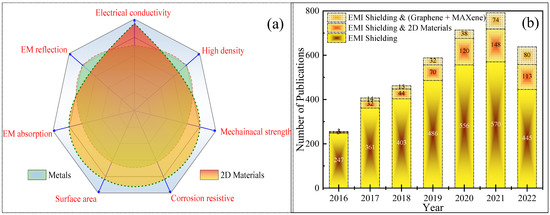
Graphene is the first two-dimensional material that becomes the center material in various research areas of material science, chemistry, condensed matter, and engineering due to its advantageous properties, including larger specific area, lower density, outstanding electrical conductivity, and ease of processability. These properties attracted the attention of material researchers resulted in a large number of publications on EMI shielding in a short time and play a central role in addressing the problems and challenges faced in this modern era of electronics by electromagnetic interference. After the popularity of graphene, the community of material researchers investigated other two-dimensional materials like MXenes, hexagonal boron nitride, black phosphorous, transition metal dichalcogenides, and layered double hydroxides, to additionally enhance the EMI shielding response of materials.

  • EMI shielding
  • shielding mechanism
  • two-dimensional materials
  • graphene
  • Microwave absorption
  • Mxene

1. Introduction

In the present day, high-frequency signals are commonly utilized for operating microprocessor-controlled electronic devices, which are at the heart of the telecommunication as well as defense sectors. These electronic devices can radiate radiations out of them, i.e., electromagnetic pollution that causes malfunctioning of nearby electrical equipment. Electromagnetic interference (EMI) is a term representing such a phenomenon where one electromagnetic wave interferes with other waves, resulting in the degradation of electromagnetic signals. EMI affects the lifetime quality as well as functioning of electronic devices. Numerous reports have been published on the adverse effects of electromagnetic pollution on biological processes in wild animals [1,2,3][1][2][3]. There are also adverse effects such as tumors, ear problems, cancer, etc., of long-term exposure to EM radiations on human health [4]. The source and effects of electromagnetic radiation are pictorially shown in Figure 1. Due to the negative effects brought on by the widespread use of electronic devices in the surroundings, EMI has become a major source of alarm. Therefore, to regulate this problem, electromagnetic shielding must be required; the shielding mechanism protects the device from the electromagnetic radiation coming from other equipment and reduces the electromagnetic pollution by absorbing the self-generated radiation also.
Figure 1. The sources of electromagnetic radiation and their effects on humans and electronics device.
The ideal material used for the shielding application should exhibit higher shielding effectiveness due to absorption along with low density, being easy to process, bulk production, low cost, being thermally stable, etc.; and possess characteristic properties like high magnetic permeability, electrical conductivity, thermal conductivity, and high aspect ratio. Therefore, there are many opportunities to produce such a material that possesses lightweight, flexible, electrical conducting, and also magnetic properties; fulfilling the needs of the modern electronics era by preventing interference from unwanted electromagnetic radiation. Stealth technology used in military equipment and fighter jets is one of the most demanding fields of highly electromagnetic radiation absorbing material. Numerous materials are being investigated for EMI shielding applications in order to meet the realistic demand for EMI shielding substances. Metals have historically been used for EMI shielding due to their great electrical conductivity. Their high density, limited mechanical flexibility, corrosiveness, and time-consuming nature, and expensive manufacturing expenses, however, limit their use. Many materials have been created and studied for EMI shielding, including metallic magnets, ferrites, ceramics, and hybrids of these materials. However, those cannot be used in the contemporary electronics era because to their high density and little flexibility.
Due to their special qualities like strong electrical conductivity, high aspect ratio, mechanical strength, etc., several two-dimensional (2D) elements are being researched for the EMI shielding application in order to get around problems like poor mechanical strength and high density. 2D layered materials including graphene, carbon nanofibers, carbon black, carbon nanotube, transition metal dichalcogenides, 2D nitrides (boron nitride and graphitic carbon nitride), layered metal oxides, MXenes, layered double hydroxides, and black phosphorus have demonstrated tremendous shielding performance and have become the front-line materials for EMI shielding in recent years. This can be understood from the comparison between metals and 2D materials with respect to the most desirable properties for the shielding material, which has been as depicted in Figure 2a.
Figure 2. (a) Metals and 2D materials are compared. (b) Developments in EMI shielding study and the role that 2D materials have played in this area (data source: Scopus).
In recent years, research in the EMI shielding field has accelerated year by year, as observed from the hike in publications displayed in Figure 2b, indicating the importance of these shielding materials. The figure also reflects the increasing demand for 2D materials in this field, as the number of 2D-material-based shielding materials publications increased from 69 to 514 in the previous six years, because of their special characteristics. Additionally, the figure demonstrates that MXene and graphene are the most-studied 2D shielding materials in the class of 2D materials.

2. EMI Shielding

Through the use of a barrier made of particular materials, EMI shielding safeguards the system from electromagnetic radiation. The barrier is performing reflection, absorption, or a combined effect of both while the electromagnetic waves are incident on it. In EMI, wresearchers consider two regions of shielding: the near-field and the far-field shielding regions. It is thought to be in the far-field shielding region when the distance between the shield and the incident electromagnetic source is larger than λ/2, where λ is the wavelength of the EM wave, and in the near-field shielding region otherwise. The participation of both electric and magnetic dipoles is implemented in the near-field portions of EMI shielding, whereas the EM plane wave theory is employed in the far-field shielding zones [5]. An abstract representation of how electromagnetic waves and a shield interact is depicted in Figure 3. The incidence of electromagnetic waves on the shield causes multiple internal reflections, reflection and absorption of waves. Electromagnetic component which is neither reflected nor absorbed is residual radiation in EMI, which emerges from the shield [6].
Figure 3. The interaction between electromagnetic waves and a shield is depicted schematically.

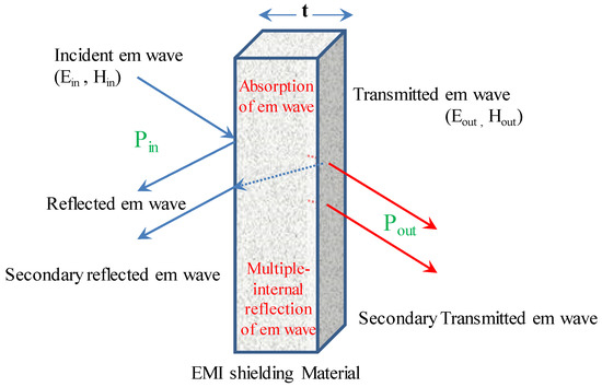
2.1. Concept of Green EMI Shielding

EMI shielding can be provided through two ways: via reflection and/or absorbing the EM radiations. The shielding due to reflection has caused one big problem because, in this phenomenon, the shield also acts as a secondary source of EM radiations. Moreover, the reflected radiations can further be free to interact with electronics devices and living bodies. As results, the chance of EM interference and other damaging effects still remains alive. Thus, the shielding due to absorption phenomena is appreciated over the reflection phenomena. Concerning the facts, Cao et al. group introduced the concept of green EMI shielding index (gs) [7,8,9][7][8][9]. The term gs (=1/|S211||S221|/|S211|1, where S11 and S12 are scattering parameters) determines the eco-friendly nature of shielding material which not only shows efficient shielding results but also controls the secondary emission of EM radiations. gs > 1 represents the less secondary emission of EM radiations and significant contribution of absorption phenomena in the shielding. Foremost, Wang et al. focused on eco-friendly shielding material and synthesized the 3D eco-mimetic nanostructure of PEDOT/Fe3O4/graphene with gs of 1.44 [7]. Zhang et al. prepared the WS2/rGO architecture that exhibits effective a green shielding effectiveness index of value > 1 [10].

2.2. Shielding Effectiveness

The ratio of the incident wave’s field strength to the transmitted wave’s field strength is known as the shielding efficacy and can be formulated as: P is the strength of the plane wave; the subscript in indicates the incident wave and out indicates the transmitted wave. A shielding material’s efficacy in blocking radiation serves as a measure of its performance (SE). Decibels are used to assess the attenuation caused by internal reflection, absorption, and other phenomena (dB). Thus, the overall shielding efficacy of a shielding substance (SET) comprises SEs contributions from reflection (SER), absorption (SEA), and multiple-reflections (SEM) and written as:
SET = SEA + SER+ SEM
The material’s permittivity and conductivity have a big impact on how well it shields. The conventional electromagnetic theory states that shielding efficacy for the thick shield of thickness ‘t’ having conductivity ‘σs’, and magnetic permeability ‘μ’ can be given as [11].
where δ is skin depth, ω is angular frequency, ε𝑜 is absolute permittivity, and μr is relative magnetic permeability of shield.
The first part of Equation (3) represents shielding effectiveness due to absorption and the second part refers to reflection. Equation (3) shows that the shielding efficacy because of absorption phenomena is directly proportional to square root of conductivity, whereas reflection is directly proportional to the logarithmic value of conductivity. Therefore, shielding performance increases with an increment in the conductivity of the material. The shielding material acquiring mobile charge carriers with lower permeability yields shielding effectiveness dominated by the reflection phenomenon. The electromagnetic wave combines with the charge carrier, causing a flow of charges and creating an electromagnetic field in opposition. The external magnetic field is cancelled out by this opposing electromagnetic field. Materials with high conductivity are used for EMI shielding. With an increasing frequency of EM radiation, the reflection loss decreases.
Because the energy of the incident wave is not lost after reflection, it serves as a secondary source of EM pollution that further disrupts the other systems. Therefore, for proper shielding, EMI shielding substance must disperse the electromagnetic signals by absorbing them. To attain EM signal absorption, shielding material have to acquire electric or magnetic properties [11].
where σs=ωε0ε(εis imaginary part of complex permittivity) and skin depth (𝛿) =1/πμσν. The distance at which the field’s strength is reduced to 1/e of its initial value is known as the skin depth. The skin depth is an interesting phenomenon correlated with the absorption of EM waves and varies inversely with respect to the electric conductivity, frequency of electromagnetic waves and magnetic permeability of shielding substance. Reflection occurs at different reflecting boundaries or surfaces inside the shielding material and is known as multiple reflections. Multiple reflections result in the scattering of electromagnetic waves. The multiple-reflection loss is negligible when the separation among interfaces is larger as compared to skin depth [12]. Also, SEM is ignored, where absorption loss is larger than a value of 10 dB.

Shielding Effectiveness Calculation

The scattering parameters S11, S12, S21, and S22 measured on a vector network analyzer (VNA) are used to calculate SE. The scattering parameters signify the strength of the reflected or transmitted signal with respect to the incident signal strength. VNA can transmit or receive as well as record the EM signal intensities over a wider frequency range. Coefficients of reflection (R), transmittance (T), and the absorption (A) for the EM signal are also calculated in terms of S-parameters as follows [13]:
R = |S11|2 = |S22|2
T = |S21|2 = |S12|2
Therefore, the SE for reflection and absorption in terms of S-parameters are given by:
Conductivity plays a crucial role in achieving higher shielding efficacy. The value of shielding efficacy required for commercial applications is 20 dB, i.e., 1% of the transmittance.

2.3. Shielding Measurement

Shielding tests are designed to determine the power of the transmitted wave passing through the shielding material. There are four basic methodologies that are usually used for shielding measurement [14]:
  • Open Field or Free Space Method;
  • Shielded Box Method;
  • Shielded Room Method;
  • Coaxial Transmission Line Method.
The most feasible way to assess the shielding power of an entire electronic assembly is through the open field method. The radiated emissions that escape the electronic device are measured in this method. This method does not measure the performance of the device due to the difference in the assembly of individual devices. In this test, the radiated emissions are recorded by mounting the device 30 m away from the receiver coil. Also, in this test, the conducted emissions that are transferred via the power lines are recorded.
For comparing measurements between the SE of various shielding substances, the shielded box method is used. The specimen is put down in the sample holder, which is mounted in a window in the wall of a metal box with a receiving antenna inside. A transmitting antenna that is placed outside the container measures the transmitted radiation intensities. The open port with the test specimen placed over it is used to gauge the strength of signals received at the transmitting antenna. The disadvantage of this procedure is the difficulty in obtaining electrical contact between both the test specimen and the metal container. Also, the range of frequency is also limited to about 500 MHz. To overcome the issues faced in the shielded box method, another method called the shielded room was developed. This method’s operation is essentially identical to that of the shielded box approach. To prevent EMI, the recorder, receiving and sending antennae and the signal generator are separated into separate rooms. The sample specimen must be expanded by an order of 2.5 m2 in size and the antennae are housed in an eco-free chamber the size of a room.
The most preferable method of EMI SE measurement is the co-axial cable transmission line method. Transmitting and receiving co-axial cables, a vector network analyzer (VNA), and a metal sample holder are used in the test setup. The losses in EM waves produced by co-axial cables are much less than antennae, and the data obtained by the co-axial cable transmission line method split into transmitted, reflected, and absorbed constituents, which is the main advantage of this method.

2.4. Factors Effecting EMI Shielding Performance

Foremost, there are two important factors impedance-matching (Zr) attenuation constant (α) that control the EMI shielding mechanism, i.e., reflection and absorption. The impedance-matching attenuation constant characteristics of the composites are governed by intrinsic characteristics, i.e., permittivity and permeability of the materials as given by Equations (10) and (11) [15]; further, the dielectric and magnetic losses are caused by both permittivity and permeability, respectively. The impedance-matching parameter control the reflection of EM radiations and flux intensity of incoming EM radiation, whereas the material’s ability to produce shielding through absorbing the radiation when EM radiations are incident and travelling through it is represented by the attenuation constant (α). According to the classical electrodynamics theory, the intensity of EM radiation decreases exponentially in the material, as I=I0eαx (I0 is initial intensity of radiation) at the propagation distance 𝑥 in the material.
where ε′ and ε″ are the real and imaginary part of complex relative permittivity. μ′ and μ″ are the real and imaginary part of complex relative magnetic permeability. The morphology, size, and thickness of the material have an impact on EMI shielding as well. Size and morphology control the electrical conductivity and dielectric properties of the material. For the shielding material, the electrical conductivity and conducting pathways inside the material are important to obtain the higher EMI shielding. It is evident from Equation (4); the thickness of the composite is directly proportional to the shielding due to absorption. According to relation I=I0eαx, as the thickness increases, the value 𝑥 increase, this assists the higher attenuation of EM radiation. Another element that influences the efficiency of the shielding is temperature. M. Cao [16] and X. X. Wang [17] et al. reported the thermally tuned EMI shielding properties of graphene-based composite material. The authors observed that the RL increased up to an optimized temperature rather than decreased, whereas EMI shielding increases with a raise in temperature. Temperature effects the charge transportation phenomena, i.e., electron hopping and migrating resulting in an increase in electrical conductivity, and, hence, conduction loss; as a result, shielding capabilities of the materials get improved. Moreover, the defects induced in the materials caused by the increase in temperature result in the attenuation of EM radiation. This is attributed to the change in structure of the material with time and temperature. The filler’s mass-to-volume ratio affects EMI shielding as well. The flexibility of the composites may be reduced by the presence of a higher filler concentration. The optimized filler concentration may increase polarization and, hence, dielectric loss, and it also increases the dielectric loss, as well as magnetic losses, resulting in enhanced dampening of EM radiation.

References

  1. Balmori, A. Anthropogenic radiofrequency electromagnetic fields as an emerging threat to wildlife orientation. Sci. Total Environ. 2015, 518–519, 58–60.
  2. Engels, S.; Schneider, N.L.; Lefeldt, N.; Hein, C.M.; Zapka, M.; Michalik, A.; Elbers, D.; Kittel, A.; Hore, P.J.; Mouritsen, H. Anthropogenic electromagnetic noise disrupts magnetic compass orientation in a migratory bird. Nature 2014, 509, 353–356.
  3. Hutchison, Z.L.; Gill, A.B.; Sigray, P.; He, H.; King, J.W. Anthropogenic electromagnetic fields (EMF) influence the behaviour of bottom-dwelling marine species. Sci. Rep. 2020, 10, 4219.
  4. Sienkiewicz, Z. Biological effects of electromagnetic fields. Power Eng. J. 1998, 12, 131–139.
  5. Yavuz, Ö.; Ram, M.K.; Aldissi, M. Electromagnetic applications of conducting and nanocomposite materials. In The New Frontiers of Organic and Composite Nanotechnology; Elsevier: Amsterdam, The Netherlands, 2008; pp. 435–475.
  6. Chung, D.D. Electromagnetic interference shielding effectiveness of carbon materials. Carbon 2001, 39, 279–285.
  7. Wang, X.; Shu, J.; Cao, W.; Zhang, M.; Yuan, J.; Cao, M. Eco-mimetic nanoarchitecture for green EMI shielding. Chem. Eng. J. 2019, 369, 1068–1077.
  8. Zhang, M.; Cao, M.; Shu, J.; Cao, W.; Li, L.; Yuan, J. Electromagnetic absorber converting radiation for multifunction. Mater. Sci. Eng. R 2021, 145, 100627.
  9. Cao, M.; Wang, X.; Zhang, M.; Cao, W.; Fang, X. Variable-Temperature Electron Transport and Dipole Polarization Turning Flexible Multifunctional Microsensor beyond Electrical and Optical Energy. Adv. Mater. 2020, 32, 1907156.
  10. Zhang, D.; Liu, T.; Shu, J.; Liang, S.; Wang, X.; Cheng, J.; Wang, H.; Cao, M. Self-Assembly Construction of WS2-rGO Architecture with Green EMI Shielding. ACS Appl. Mater. Interfaces 2019, 11, 26807–26816.
  11. Farukh, M.; Dalal, J.; Ohlan, A.; Singh, K.; Dhawan, S.K. Synthesis of Poly (3, 4-ethylene dioxythiophene) Conducting Polymer Composites for EMI Shielding Applications. Bentham Sci. 2022, 213–270.
  12. Dalal, J.; Gupta, A.; Lather, S.; Singh, K.; Dhawan, S.K.; Ohlan, A. Poly(3, 4-ethylene dioxythiophene) laminated reduced graphene oxide composites for effective electromagnetic interference shielding. J. Alloys Compd. 2016, 682, 52–60.
  13. Dalal, J.; Malik, S.; Dahiya, S.; Punia, R.; Singh, K.; Maan, A.S.; Dhawan, S.K.; Ohlan, A. One pot synthesis and electromagnetic interference shielding behavior of reduced graphene oxide nanocomposites decorated with Ni0.5Co0.5Fe2O4 nanoparticles. J. Alloys Compd. 2021, 887, 161472.
  14. Yang, Z.; Peng, H.; Wang, W.; Liu, T. Crystallization behavior of poly(ε-caprolactone)/layered double hydroxide nanocomposites. J. Appl. Polym. Sci. 2010, 116, 2658–2667.
  15. Kumari, S.; Dalal, J.; Kumar, A.; Ohlan, A. Microwave Absorption Performance of Core–Shell rGO/Ni0.5Co0.5Fe2O4@PEDOT Composite: An Effective Approach to Reduce Electromagnetic Wave Pollution. Adv. Eng. Mater. 2022, 24, 2200635.
  16. Cao, M.; Wang, X.; Cao, W.; Fang, X.; Wen, B.; Yuan, J. Thermally Driven Transport and Relaxation Switching Self-Powered Electromagnetic Energy Conversion. Small 2018, 14, 1800987.
  17. Wang, X.X.; Zhang, M.; Shu, J.C.; Wen, B.; Cao, W.Q.; Cao, M.S. Thermally-tailoring dielectric “genes” in graphene-based heterostructure to manipulate electromagnetic response. Carbon 2021, 184, 136–145.
More
Video Production Service