Your browser does not fully support modern features. Please upgrade for a smoother experience.
Please note this is a comparison between Version 2 by Catherine Yang and Version 1 by Sixian Wu.
Through ceramic via (TCV) technology expands the volume of high-precision and high-power thin-film circuits with 3D planar distribution, significantly improves the structural density and reduces the device size through via interconnection and circuit redistribution. Through glass via (TGV) technology has the advantages of high-density interconnection and low-loss transmission, which forms a highly reliable interconnection between the chip and the substrate, has higher I/O density and smaller spacing, and realizes passive on-chip devices, high-density copper interconnection and the heterogeneous integration of chips. Therefore, 3D integration and system-level packaging technology have developed rapidly.
- TSV
- TGV
- TCV
- process optimization
1. Introduction of TCV
Due to ceramics’ advantages in terms of high thermal conductivity, high heat resistance, high electrical insulation, high mechanical strength, a low coefficient of thermal expansion (CTE), excellent corrosion resistance and radiation resistance, TCV is a new interconnection technology used in high-density three-dimensional packaging and maximizes the structural density in three dimensions. Under the same size, TCV technology can create more devices with good high-frequency performance, which provides a solution for micro-system power supply circuits, passive component integration and the high-density combination of multifunctional devices and units [75][1].
1.1. Process Flow Design
The integration process of TCV has been improved and developed on the basis of the traditional thin-film manufacturing process, while common technologies such as metallization, lithography, development, corrosion, electroplating and integrated resistance are important links. The core technologies that TCV needs to pay attention to are micro-vias, full-hole metallization, multi-layer wiring, 3D ceramic stacking and so on [76][2]. In addition, special attention should be paid to the compatibility of the multi-process and implementation process on general technologies and key technologies. The manufacturing process of TCV is shown in Figure 31. A ceramic via is formed on a silicon substrate by laser ablation. This maskless process simplifies the preparation process of the via and does not require photolithography. Next, the dielectric resin is filled, and a thick dielectric layer is formed through the second through hole drilling. Then copper plating is carried out and SR coating is added for high-temperature wear protection, and finally, the whole surface is cleaned [76][2].
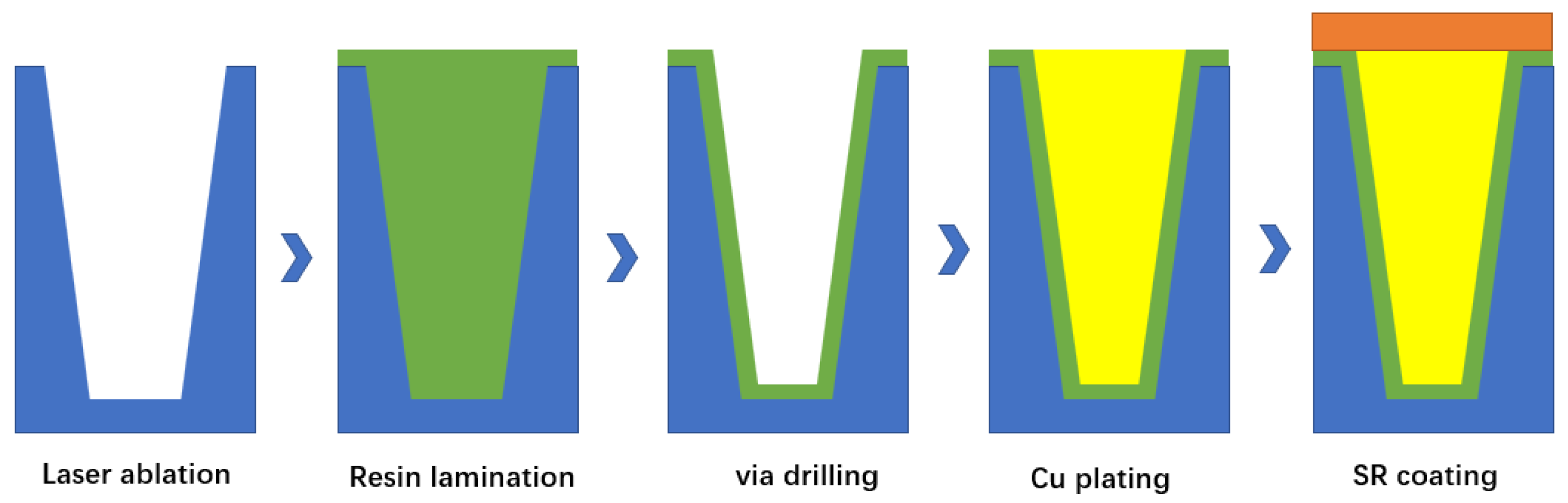
Figure 31.
The TCV process flow chart.
The 3D stacking of TCV technology is realized by connecting ceramic perforations between hierarchical substrates. The traditional thin-film process usually uses laser drilling and sputtering metallization processes to prepare hollow grounding holes. This method can not meet the requirements of flip chip solder balls and high-frequency signal transmission between TCV layers, so it is necessary to study the preparation process of solid holes for 3D ceramic connection. The following two solutions can form 3D communication holes in ceramics.
- (1)
-
Slurry filling
Due to the consistency between the substrate and the paste, solid through holes can be formed in Al2O3, and the ceramic substrate can be filled with reference to the paste printing process. Coating a template on a ceramic substrate, coating paste in holes with a scraper, and then drying and sintering to obtain a substrate with through holes filled with slurry. The schematic diagram is shown in Figure 32 [18][3].
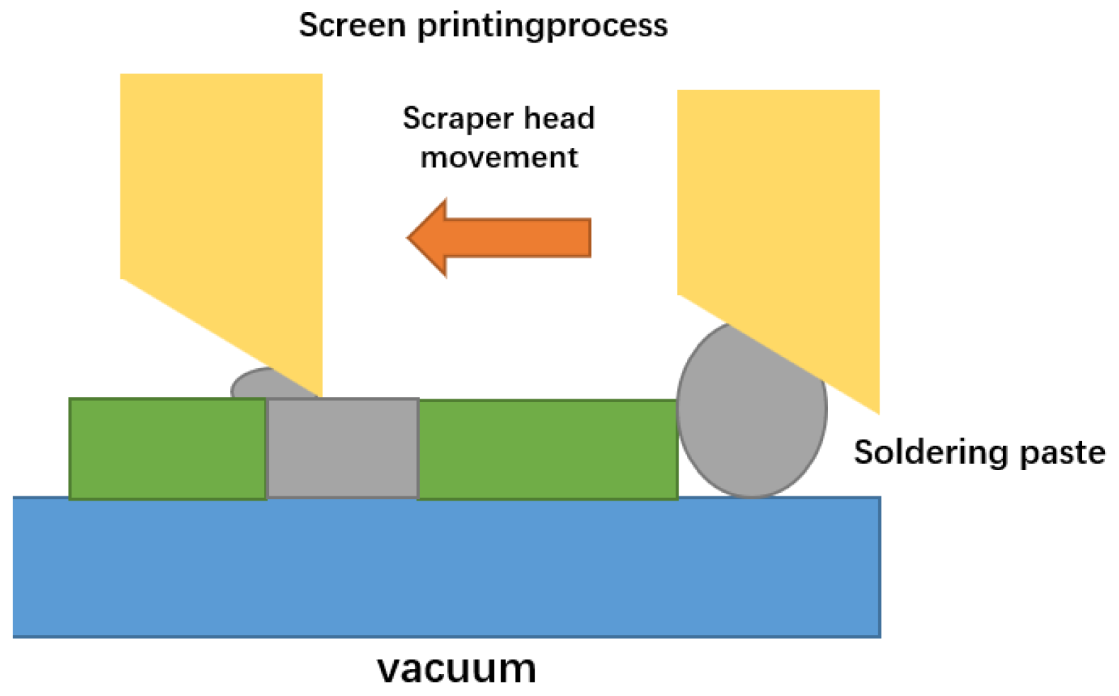
Figure 32.
Schematic diagram of slurry printing hole filling.
- (2)
-
Electroplating filling
Inspired by the concept of TSV, TCV can also fill the through hole by deep hole electroplating, which can achieve the advantages of good air tightness and excellent conductivity. However, this scheme also has some shortcomings because in the process of deep hole electroplating, the exchangeability of the solution in the hole is poor, and the electroplating speed on the surface of the hole is higher than that on the inner wall, so it is easy to form a mushroom-like filler or to seal it in advance to make it a hollow hole. Therefore, by optimizing the electroplating parameters and reducing the difference in electroplating speed between the hole surface and the hole, the solid hole could be filled in the study [77][4].
1.2. TCV Process Optimization and Reliability
This technology is still in its infancy in China. In terms of new technologies, 3D laser processing, deep groove etching and photosensitive glass cutting could be developed and applied. In addition to ceramic substrate stacking in the material system, heterogeneous stacking of different substrates (such as glass and sapphire) can also be developed, providing increasingly effective solutions for multi-functional heterogeneous integration and micro-system integration.
Qiang Wang et al. [78][5] researched filling-based DC optimization. Chronoamperometry and solution conductivity measurements were used to optimize the electroplating solution. The through hole section’s electroplating effect was used to estimate process parameters such as current density and air stirring flow rate. The optimized solution included 120 g/L CuSO4, 55 g/L H2SO4, 50 mg/L Cl−, 200 mg/L PEG8000, 7 mg/L SH110 and 6 mg/L NTBC.
To optimize the thermo–mechanical reliability of the ceramic substrate with an in-line copper-filled TCV structure, Tingrui Gong et al. [75][1] employed the Taguchi–Grey approach and finite element modeling. On the thermal stress of TCV, the effects of six design parameters—TCV diameter, TCV height, spacing, substrate material, metal layer thickness and substrate cross-sectional area—were analyzed. For thermal stress, the order of these six factors was: the substrate material > diameter > the pitch > the metal layer thickness > the TCV height > substrate cross-sectional area. The proportion of substrate material, TCV diameter and pitch was relatively large—46.7%, 26.49% and 9.38%, respectively.
2. Introduction of TGV
The appearance of a glass-based transfer plate provides another choice for people. Glass material is an insulating material with a low loss coefficient and excellent electrical properties. In addition, when metal is filled with TGV, the sidewall does not need to be oxidized and insulated, thus reducing the production cost. Therefore, TGV technology has broad application prospects in the field of 3D MEMS packaging, especially its technical advantages of small size and no leads, which makes the TGV technology have application potential of miniaturization and high reliability in aerospace equipment [79][6].
2.1. The TGV Process
TGV, that is, the glass adapter plate, punches holes in the glass and the electroplate’s copper columns to realize the communication between the upper surface and the substrate. As shown in Figure 33, it realizes the transformation from a two-dimensional planar circuit to a 3D circuit, and further promotes the integration of passive devices [80][7].
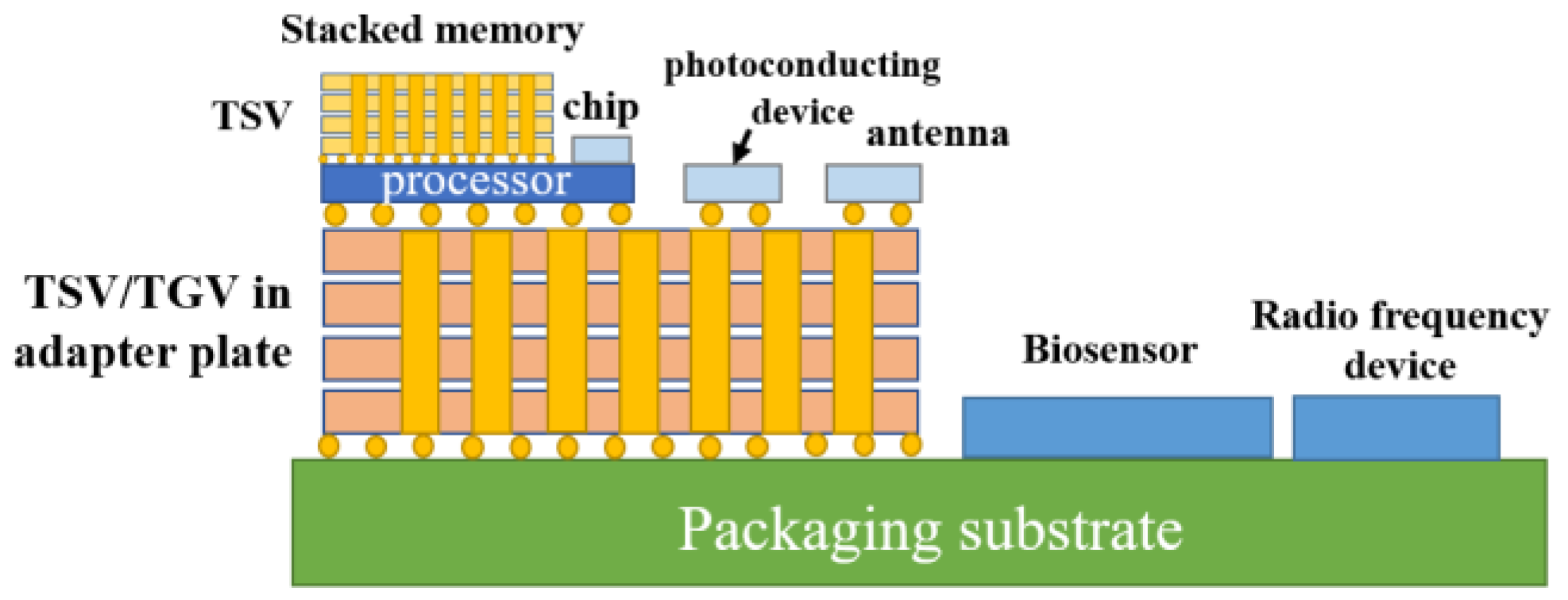
Figure 33.
Application of TSV/TGV adapter board in a 3D integrated circuit.
The silicon wafer is engraved with a deep groove with a certain depth, and the glass sheet is covered on the grooved silicon wafer surface, while the anodes are bonded together in a vacuum environment. Heat at high temperature to soften the glass and under the action of atmospheric pressure, the glass flows into the tank until it is full; double-sided CMP exposes the silicon conductive column. The silicon conductive column can realize the longitudinal interconnection of electrical signals, and the lead wire does not need to pass through the sealing ring, which can better realize vacuum sealing. The two processes shown in Figure 34 are the glass reflow process and the glass thermal reflow process; one of the new methods to realize the TGV packaging structure. Its typical process route is called glass-in-silicon reflow (GISR) [81][8].
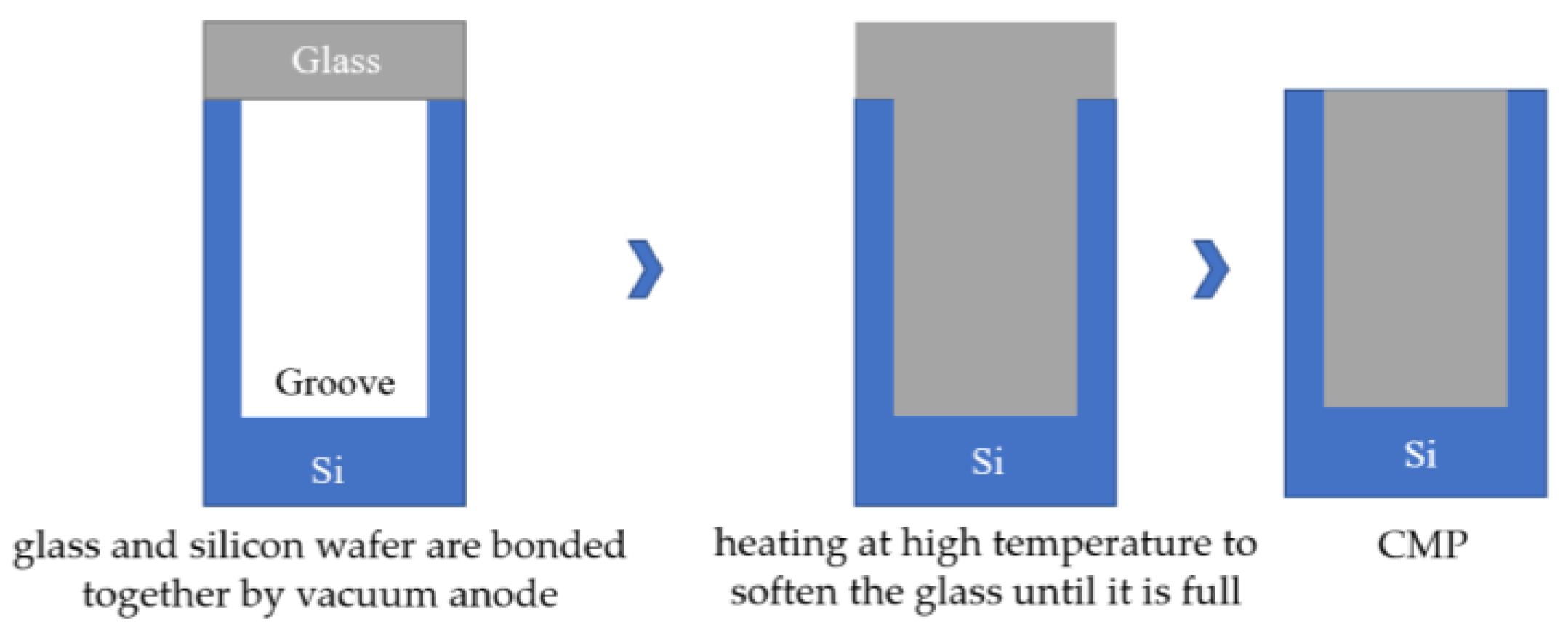
Figure 34.
Schematic diagram of the basic manufacturing process of TGV substrate.
At present, the research on TGV technology based on glass reflow is hot at home and abroad, while MEMS packaging schemes and products based on TGV technology are constantly proposed and realized. For example, Sensonor Technologies AS has proposed and produced a butterfly wing silicon micro-gyroscope based on glass reflow TGV packaging, and Peking University has proposed a three-layer wafer-level vacuum packaging scheme based on TGV technology, which can fill silicon deep grooves with feature sizes as small as microns. Wafer-grade borosilicate glass is widely used as a thermal reflow glass material because of its adaptive thermal expansion coefficient, good insulation and optical properties. In the GISR process, reflux temperature and holding time are the most important parameters. The process flow chart of high-density TGV is shown in Figure 35 [82][9] and comprises the following basic process steps:
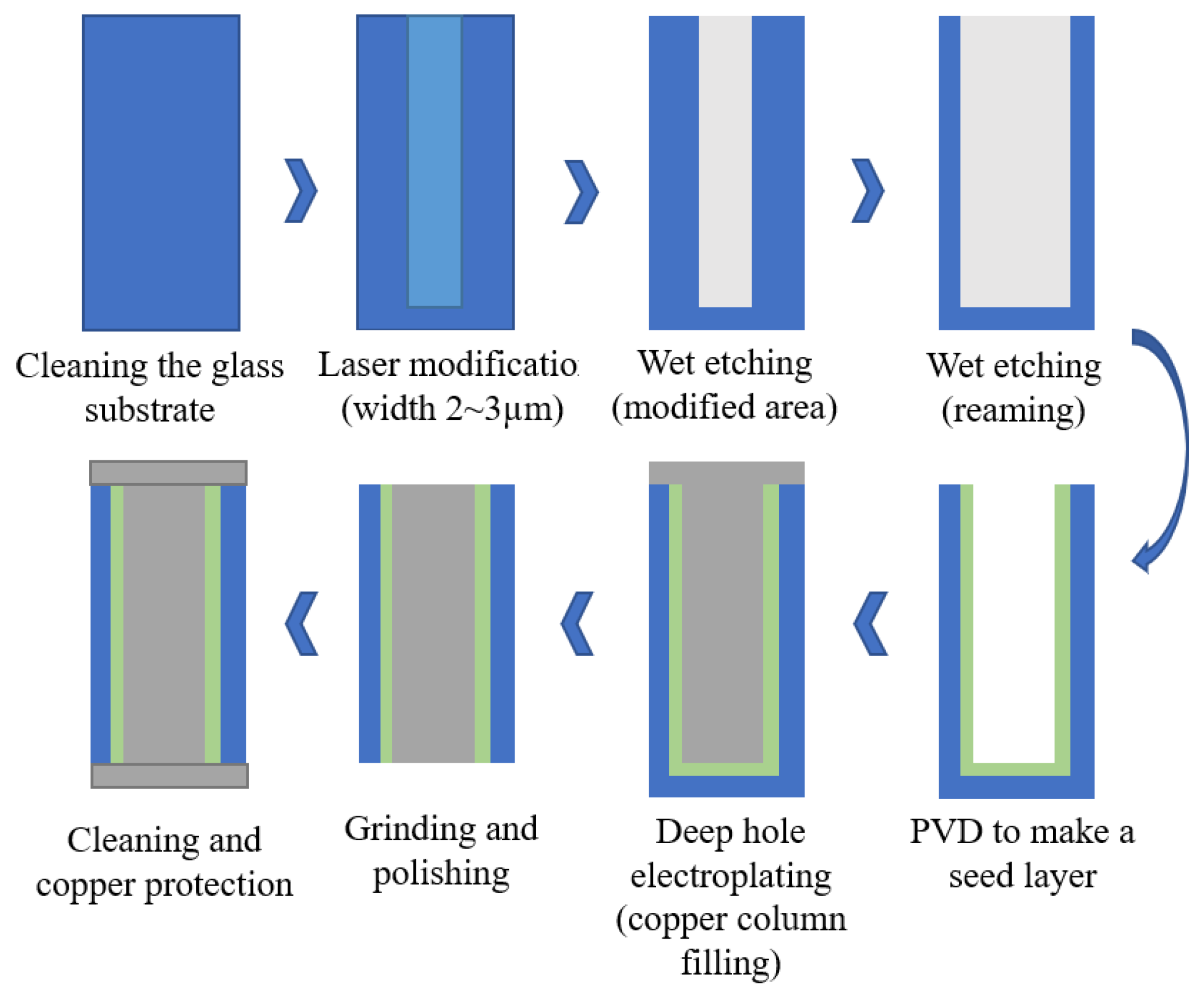
Figure 35.
The process flow chart of high-density TGV.
- (1)
-
Selective laser modification is carried out on the clean glass substrate. The high-energy and high-power density laser focused inside the glass breaks the silicon–oxygen bond and forms a micro-activated region with a diameter of 2~3 μm on the glass substrate;
- (2)
-
Then, the laser-modified substrate is wet etched by using a strong alkaline etching solution with a certain concentration. In the etching process, the uniformity of the etching solution is maintained by stirring and ultrasonic wave. The heating temperature is adjusted to control the reaction speed and the etching time accurately so as to obtain a through hole;
- (3)
-
Then a seed layer with a Ti–Cu structure with good adhesion to the inner wall of the through hole and the surface of the substrate is deposited by physical vapor deposition (PVD);
- (4)
-
Copper is plated on the surface of the through hole and the substrate through the deep hole electroplating process. Considering the huge difference in the thermal expansion coefficient between the glass and copper, in order to avoid the thermal mismatch between the copper column and glass substrate under high power conditions, the high temperature of the transfer plate could lead to the fracture of the transfer plate; however, through hole electroplating is carried out by a partially hollow process. The copper column in the through hole is not completely filled, leaving gaps at both ends of the copper column, which provides space for thermal expansion of the copper column under high power conditions;
- (5)
-
Grinding the copper on the thinned surface with micron-sized grinding media: nano-alumina powder is used to polish and remove copper and crystal layer on the surface to ensure the smooth and clean surface of the substrate; Finally, clean the surface of the substrate and remove impurities (organic materials and polishing liquid residues attached to the surface), and use a copper protective agent to form a protective film on the upper and lower surfaces of the copper column to prevent the copper surface from oxidation.
2.2. TGV Process Optimization
The main results are as follows:
- (1)
-
GISR process parameter optimization
The research on GISR technology mainly focuses on the design and implementation of the whole package scheme, and there are few documents about the details of the glass reflow process. A general model and equation considering the details of groove width, groove depth, temperature and time have not been established. Therefore, Qijun Hu et al. [81][8] proposed and established a general model of glass reflow by studying the effects of gap depth, gap width, temperature and time parameters on glass reflow. The relationship between the flow length and time of the glass in the microchannels under a specific groove width, groove depth and temperature was derived. Xiaohui Du et al. [83][10] used a nano-glass powder reflow process to prepare a TGV structure for leadless packaging so that a better nano-glass powder process and high-temperature reflow process parameters were obtained. The refluxed glass can effectively fill the large plane groove with silicon columns and the groove with high aspect ratio, and the lower corner of the groove can be completely filled without bubbles in the glass block.
- (2)
-
Optimization of TGV heat dissipation structure
Because the thermal conductivity of the glass substrate is 0.52~1.28 W/(m·k), the low thermal conductivity finds it difficult to meet the high-efficiency heat dissipation requirements of high-power microwave devices. Therefore, it is necessary to make full use of the good heat dissipation characteristics of metallic copper, to design a high-density copper column arrangement for the glass transfer plate and form a TGV heat dissipation structure to improve the heat dissipation ability, thus, ensuring good reliability of the TGV transfer plate packaging and integration. Therefore, Qiangwen Wang et al. [82][9] designed and analyzed the heat dissipation structure of TGV according to the high heat dissipation performance requirements of TGV. The finite element model of the TGV adapter plate packaging integrated structure was established, the heat dissipation structure of the TGV adapter plate copper column array was designed, and the TGV high-density array was made by the TGV process, as shown in Figure 36.
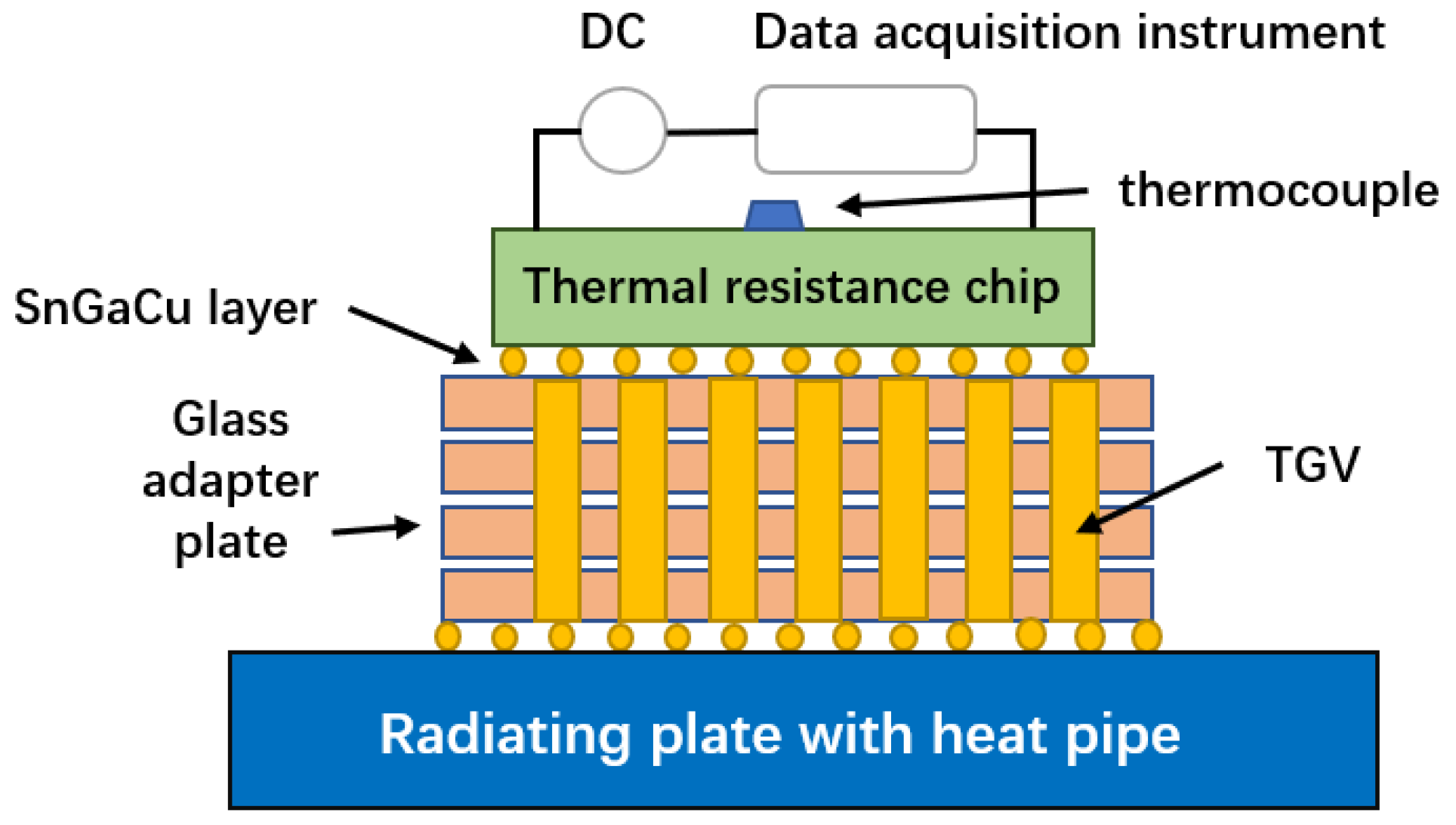
Figure 36.
Schematic diagram of the test method for heat dissipation performance of the TGV adapter plate.
- (3)
-
Optimization of TGV process parameters
There are two kinds of thermo–mechanical induced cracks in metalized TGV substrates: radial cracks and circumferential cracks. Radial cracks are formed during heating, while circumferential cracks are formed during cooling. However, radial cracks have higher reliability problems because they may lead to catastrophic failure due to the network of adjacent cracks. Therefore, Chukwudi Okoro et al. [84][11] understood and eliminated the formation of radial cracks. Their results showed that the number of radial cracks increased with the increase of heating rate, and the dependence of radial crack probability on the applied annealing rate followed an exponential function. When the heating rate was less than 6.5 °C/min, no cracks were formed; that is, radial cracks were eliminated. In order to study the stress relaxation activity, the functional relationship between the copper protrusion height of TGV and the annealing heating rate was measured, as shown in Figure 37. Jin Zhao et al. [85][12] discussed the cracks in the 3D-TGV interconnection structure through experiments and numerical simulation. The influence of geometry and material characteristics on the TGV interconnection was studied by the finite element method. Finally, some technological processes and improvement measures were put forward. The results showed that the copper protrusion decreased with the increase of the heating rate. This means that at a faster heating rate, less stress is released. However, at a lower heating rate, the large protrusion of Cu led to the reduction of the Cu volume of extruded glass substrate, thus reducing the induced substrate stress and minimizing the possibility of forming radial cracks.
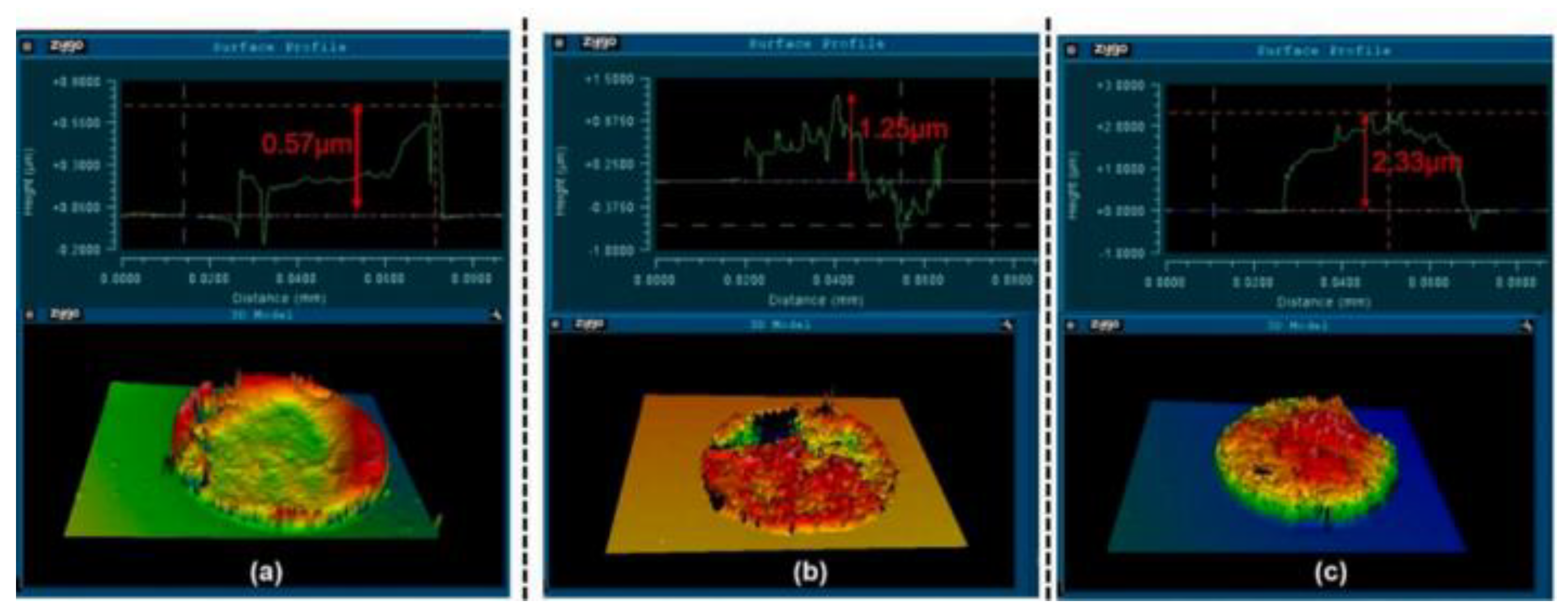
Figure 37.
The measurement of Cu protrusion height by heating rate (
a
) 26 °C/min; (
b
) 13 °C/min; (
- (4)
-
Optimization of the preparation process of the TGV glass seed layer
Complete filling can reduce potential risks, improve the reliability of signal transmission and reduce energy loss. Because of the low processing temperature, low processing cost and simple manufacturing and processing, chemical plating is a common method for preparing the seed layer. Yuzhe Chen et al. [86][13] realized a method of preparing the glass seed layer by nickel colloid activation and electroless nickel plating. In order to improve the characteristics of the seed layer, the nickel activation process was optimized comprehensively. A detailed annealing treatment was carried out to improve the adhesion of contact points. After optimization, the deposition of the Ni–P seed layer obtained good coverage and contact adhesion.
2.3. Development of TGV Technology
Glass materials have greater potential in the miniaturization of passive devices such as filters and inductors, and TGV technology has a greater potential in chip packaging applications. The development of glass-based technology has yet to be developed, and other high-performance, miniaturized RF devices, such as AIP packaged antennas, high Q chip inductors and power splitters, can also be made by using glass substrates.
For the 3D integration process, the technical development of TGV has not been widely studied at home and abroad, and its reliability research needs to be optimized. It is the key direction of TGV 3D integration in the future to realize the complete process of glass substrate RF devices to 3D packaging through glass bonding technology.
The modeling of the TGV process is not perfect, and the simulation analysis of interlayer capacitance, contact resistance and conductivity needs to be refined. The loss caused by the process can be further improved through model analysis.
3. Process Limitation
The TCV and TGV processes are used in semiconductor packaging to create vertical interconnections through chips or substrates. However, these processes have certain limitations in terms of via diameter, via height, aspect ratio and via cavity. An explanation of these limitations is discussed below.
A larger hole diameter can provide a lower resistance and voltage drop, so it can carry a higher current. This is particularly important in high-power applications and high-frequency signal transmission. A smaller hole diameter can reduce signal crosstalk and signal losses and improve signal reliability and transmission quality. Especially in high-speed communication and microwave applications, a smaller hole diameter can reduce signal distortion and transmission delay and improve system performance.
A higher hole height will lead to larger resistance and capacitance, increase the delay and loss of signal transmission, and may also lead to uneven material filling, holes, poor filling, or material accumulation, and lead to more fragile and easily damaged interconnection structures that are prone to stress concentration and fracture. A lower hole height can reduce the resistance and capacitance, improve the speed and quality of signal transmission, and realize uniform filling and coating more easily. It can also increase the mechanical stability and strength of the interconnection structure so as to improve the stability of the process and the reliability of the products.
A comprehensive evaluation of the ratio of height to diameter shows the influence of the aspect ratio: a higher aspect ratio may lead to uneven distribution of filling and coating materials in the interconnection holes, and also lead to greater signal transmission delay and loss, which may affect the transmission quality and system performance of high-frequency signals. A higher aspect ratio may lead to more fragile interconnection structures and easy stress concentration. A lower aspect ratio not only makes it easier to achieve uniform filling and coating but also improves the mechanical strength and stability of the interconnection structure and can also reduce the crosstalk and loss of the signal and improve the signal integrity.
In practical applications, it is necessary to comprehensively consider the influence of these factors on electrical performance, manufacturing cost, signal integrity and structural stability.
References
- Gong, T.; Qin, F.; Yan, X.; Gao, L.; Yang, Y.; Lei, Z.; Tan, H.; Li, J. Thermo-mechanical optimization of ceramic substrate with through ceramic vias by Taguchi-Grey method. Microelectron. Reliab. 2022, 132, 114535.
- Takahashi, K.; Sekiguchi, M. Through Silicon Via and 3-D Wafer/Chip Stacking Technology. In Proceedings of the 2006 Symposium on VLSI Circuits, Honolulu, HI, USA, 15–17 June 2006.
- Qin, Y.-L.; Wang, C.-F.; Li, Y.-R.; Gao, Y.; Liao, A. Through Ceramic Via(TCV)Interconnection Technology. Electron. Process Technol. 2017, 38, 4.
- Yang, J.-P.; Zhou, J.; Shne, G.-C.; Wu, J.; Shen, Y.; Cai, M. RF Characterization of TSV Vertical Transition Structure. Res. Prog. Solid State Electron. 2016, 5.
- Wang, Q.; Cheng, T.; Chen, F.; Cheng, M. Study on direct current Cu electroplating in through ceramic holes for high-power LED packaging. In Proceedings of the 2020 21st International Conference on Electronic Packaging Technology (ICEPT), Guangzhou, China, 12–15 August 2020; pp. 1–5.
- Topper, M.; Ndip, I.; Erxleben, R.; Brusberg, L.; Reichl, H. 3-D Thin film interposer based on TGV (Through Glass Vias): An alternative to Si-interposer. In Proceedings of the 2010 Proceedings 60th Electronic Components and Technology Conference (ECTC), Las Vegas, NV, USA, 1–4 June 2010.
- Chen, Y.-Z. Research of On-Chip Inductor Based on TGV Technology; University of Electronic Science and Technology of China: Chengdu, China, 2022.
- Hu, Q.-J.; Zhou, J.; Li, W.-Y.; Hou, Z.-Q.; Xiao, D.-B.; Wu, X.-Z. Modeling of glass-reflow facing TGV substrate. Transducer Microsyst. Technol. 2017, 36, 4.
- Wang, W.-Q.; Guo, Y.-H.; Liu, J.-J.; Wang, Y.-L. High Heat Dissipation Performance of the TGV Interposer. Micronanoelectron. Technol. 2021, 58, 7.
- Du, X.-H.; Liu, S.; Zhu, M.-J. Reflow Technology of Nano-Glass Powder for TGV Packaging. Micronanoelectron. Technol. 2020, 57, 6.
- Okoro, C.; Jayaraman, S.; Pollard, S. Understanding and eliminating thermo-mechanically induced radial cracks in fully metallized through-glass via (TGV) substrates. Microelectron. Reliab. 2021, 120, 114092.
- Zhao, J.; Chen, Z.; Qin, F.; Yu, D. Thermo-Mechanical Reliability Study of Through Glass Vias in 3D Interconnection. Micromachines 2022, 13, 1799.
- Chen, Y.; Zhang, J.; Gao, L.; Zou, S.; Liang, K.; Liu, Z.; Fang, Z.; Chen, H.; Ye, Q. An optimized NiP seed layer coating method for through glass via (TGV). Microelectron. Eng. 2022, 257, 111735.
More