Your browser does not fully support modern features. Please upgrade for a smoother experience.
Submitted Successfully!
 +1 credit
Thank you for your contribution! You can also upload a video entry or images related to this topic.
For video creation, please contact our Academic Video Service.
| Version | Summary | Created by | Modification | Content Size | Created at | Operation |
|---|---|---|---|---|---|---|
| 1 | Xiaoxiao Wang | + 2138 word(s) | 2138 | 2021-05-19 08:19:35 |
Video Upload Options
We provide professional Academic Video Service to translate complex research into visually appealing presentations. Would you like to try it?
Cite
If you have any further questions, please contact Encyclopedia Editorial Office.
Wang, X. Phase-Change Materials. Encyclopedia. Available online: https://encyclopedia.pub/entry/9839 (accessed on 23 June 2026).
Wang X. Phase-Change Materials. Encyclopedia. Available at: https://encyclopedia.pub/entry/9839. Accessed June 23, 2026.
Wang, Xiaoxiao. "Phase-Change Materials" Encyclopedia, https://encyclopedia.pub/entry/9839 (accessed June 23, 2026).
Wang, X. (2021, May 19). Phase-Change Materials. In Encyclopedia. https://encyclopedia.pub/entry/9839
Wang, Xiaoxiao. "Phase-Change Materials." Encyclopedia. Web. 19 May, 2021.
Copy Citation
Phase-change materials (PCMs) are important photonic materials that have the advantages of a rapid and reversible phase change, a great difference in the optical properties between the crystalline and amorphous states, scalability, and nonvolatility.
phase change materials
photonic devices
reconfigurable
modulator
optical switch
optical logic devices
vanadium dioxide
chalcogenide
photonic neural networks
1. Introduction
The most attractive PCMs are chalcogenide compounds (e.g., Ge2Sb2Te5, GeTe, and Ge–Sb–Se–Te) and transition-metal oxides (e.g., VO2 and NbO2). There are distinct differences between PCMs, such as the volatility, refractive index contrast before and after the phase change, and phase-transition speed [1]. Ge2Sb2Te5 (GST) is a commonly used PCM with fast crystallization speed, large optical and electrical contrast, and good reversibility between the amorphous and crystalline states. The amorphous GST film exhibits semiconductor characteristics, while crystalline GST films exhibit semimetallic and metallic properties in different crystalline states at specific temperatures. The characteristic material of another type of PCM is vanadium dioxide (VO2). By increasing the temperature, VO2 undergoes an insulator-to-metal transition around its phase-transition temperature, so VO2 has substantial optical contrast [2]. Upon decreasing the temperature of VO2 below the phase-transition temperature, its state reverts back to the initial structure [3]. As a result, VO2 is unsuitable for nonvolatile and reconfigurable applications. Therefore, PCMs can help to realize novel photonic devices and catch up with the requirements for a higher level of integration, adjustability, and performance [4].
2. GST and Other Chalcogen-Based Optical PCMs
2.1. Models and Physical Mechanism of the Phase Transitions of GST
Kolobov et al. [5] developed a model to explain the mechanism of the phase-transition process of the GST alloy that fits the experimental data well. The distinction between the two states was measured by extended X-ray absorption fine-structure spectroscopy and Raman scattering spectroscopy to construct the model and explain the mechanism. The obtained results (Figure 1a,b) were in good agreement with previous X-ray diffraction measurements.
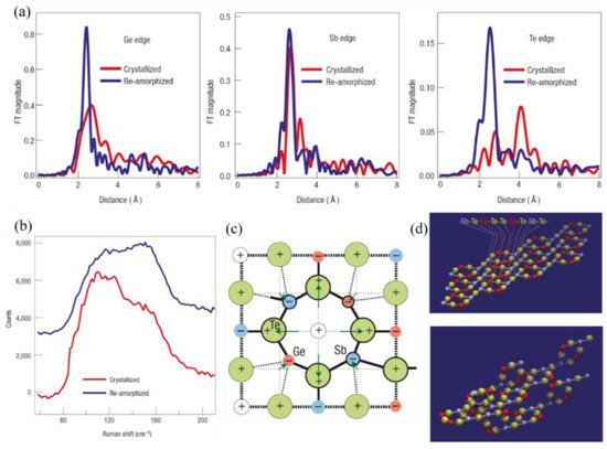
Figure 1. The models and physical mechanism of Ge2Sb2Te5 (GST) phase transitions. (a) Fourier-transformed raw extended X-ray absorption fine-structure spectroscopy (EXAFS) spectra for crystallized and laser-amorphized samples. Spectra measured at the K-edges of Ge, Sb, and Te. On amorphization, the bonds become shorter (as shown by shifts in the peak positions) and stronger, that is, more locally ordered (as shown by increases in the peak amplitudes and concurrent decreases in the peak widths). (b) Raman scattering spectra for crystallized and re-amorphized GST layers. (c) The crystal structure of laser-amorphized GST. A schematic two-dimensional image of the lattice distortion of the rocksalt structure due to charge redistribution between the constituent elements. (d) The ideal structure of GST, constructed from the above building blocks and fragments of the three-dimensional GST structure constructed from rigid building blocks.
They determined that the true structure of the crystalline phase is not a typical type of rock-salt structure, although it is similar. The Ge and Sb atoms may swap places, producing randomness, and each additional building block may rotate by 90° in an arbitrary direction. In addition, the ideal model exhibits a stacking sequence of –Sb–Te–Ge–Te–Te–Ge–Te–Sb–Te–, which is identical to the stable hexagonal structure of GST, thus predicting the phase change to some extent. The structure is shown in Figure 1c.
Laser-induced amorphization results in a drastic shortening of covalent bonds of GST (Te–Ge and Te–Sb bonds) and a decrease in the mean-square relative displacement, demonstrating a substantial increase in the degree of short-range order. To obtain further insight into the amorphous structure, Kolobov et al. [5] performed X-ray absorption near-edge structure simulations. The mechanism of the phase transition can be explained as follows. The Ge atoms play a key role in the amorphization procedure. They occupy the octahedral and tetrahedral symmetry positions in the crystalline and amorphous states, respectively. The difference is that several weaker covalent bonds connect the Ge atoms with other atoms. Upon application of an intense laser, the weaker bonds will be ruptured, and the Ge atom will flip into the tetrahedral position. By checking the Ge–Te distance, this explanation fits the experimental data well. They suggested that electronic excitation creating nonequilibrium charge carriers is crucial for weakening and subsequent rupture of the subsystem of weaker Ge–Te bonds. Photogenerated nonequilibrium carriers populate these states, making them more susceptible to thermal vibration-induced dissociation. The local arrangement around the Sb atoms remains unchanged, enhancing the overall stability. Both of these factors contribute to amorphization.
2.2. Properties of GST and Other Chalcogen-Based Optical PCMs
GST is widely used and commercialized in materials that are used in optical data storage devices, such as digital videodisks (DVDs). Researchers are attempting to discover new properties while searching for new applications of the currently known properties of GST. By slightly changing GST and exploring its new properties, research has been extended from GST to some general chalcogen-based optical PCMs (O-PCMs).
Chalcogen-based PCMs consist of some particular elements that are widely used for memory. The commonly used elements are shown in Figure 2a [6]. Other than these elements, researchers have also discovered other components that have potential phase-change properties; for example, AuTe2, which is also included in the chalcogen-based materials family.
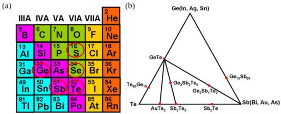
Figure 2. (a) Typical elements in the chalcogenide family used for optical storage. (b) The tertiary Ge-Sb-Te phase diagram with some popular chalcogenide alloys highlighted.
The discovery of a new class of materials along the GeTe–Sb2Te3 pseudo-binary line brought about the initial use of GST alloys. The basic properties were known long before, and it was not until the emergence of the pseudo-binary line that GST alloys attracted much attention because of their properties. Alloys along this line with compositions (GeTe)m(Sb2Te3) have the ability to rapidly switch between the phases and have strong electrical/optical contrast [7]. After doping the material with elements (mostly those in Figure 2a, crystallization will change, which could result in an even faster switching speed or a steadier amorphous phase [20,21]. The GeTe–Sb2Te3 pseudo-binary line and the previously mentioned alloys are shown in Figure 2b [6].
GST alloys and other chalcogen-based PCMs have similar optical properties that are beneficial for potential applications. They work by forward crystallization and backward amorphization, which is a way of phase transformation that is reversible. The procedure is shown in Figure 3 [8]. The two states of these materials show tremendous contrast of the optical constants. We mostly pay attention to the complex index of refraction, optical loss, and electrical resistivity [9]. These properties are fundamental to optical storage, light modulators, and other types of devices.
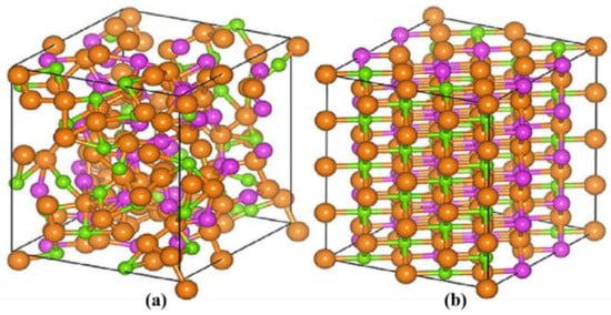
Figure 3. The structural phase transition of the GST chalcogenide PCM between its (a) amorphous and (b) crystalline states.
The phase-change process is based on the thermal effect. By applying a specifically designed laser pulse, the material will be heated above its crystallization temperature but below its melting point. After slow cooling, in contrast to amorphization, the atoms will show long-range order, so the material is in the crystalline state. If the material is heated above the melting point and then rapidly quenched to room temperature, it will reach the amorphous state. The two states have different electronic densities and transition matrix elements, that is, the oscillator strength of the optical transitions due to structural rearrangement. Another advantage of GST alloys and other chalcogen-based PCMs is that the phase-change processes of these materials can be very fast, and they are faster than those of almost all known materials.
Other properties are also important for this type of material to be used in devices. Requirements such as stability at room temperature, large scalability of the capacity, a nonvolatile nature, and extended read/write endurance are all fulfilled by GST alloys and other chalcogen-based PCMs, and they are necessary for applications.
In addition to the optical properties, the thermal properties should also be taken into consideration. The thermal conductivities of the different phases of Ge2Sb2Te5 range from 0.14 to 1.76 W/(m·K) [10]. The low thermal conductivity can significantly reduce energy consumption in the crystallization and amorphization procedure, which is beneficial for the optical properties.
3. VO2 and Other Transition-Metal Oxide O-PCMs
3.1. Models and Physical Mechanism of the Phase Transitions of VO2
VO2 is one of the strongly correlated electron materials that are typically characterized by a variety of phase transitions that occur as a result of competing interactions between the charge, spin, orbital, and lattice degrees of freedom [11]. First-order phase transitions in solids, such as VO2, are notoriously challenging to study [12]. The transition-metal dioxides at the beginning of the d series have been studied by DFT-based electronic structure calculations, which are capable of correctly describing the electronic and magnetic properties of the metal, as well as both the first insulating monoclinic (M1) and the second insulating monoclinic (M2) phases. By using recently developed hybrid functionals, considerable progress has been made in understanding the physics of VO2, including the electron–electron interaction, and thereby improving the weaknesses of the semilocal exchange functionals provided by the local density and generalized gradient approximations [13]. Although there are limitations in the local density approximation, the theory establishes a reference that can be directly compared with experimental data [14].
The results of calculations based on DFT using hybrid functionals are shown in Figure 4b,c, which are in good agreement with the experiment. The group of bands straddling the Fermi energy is dominated by the V3d states. The V3d and O2p contributions in the energy range, where the respective other orbitals dominate, result from hybridization between these states. Therefore, the phase transition is accompanied by strong orbital switching, which has been confirmed by polarization-dependent X-ray-absorption spectroscopy measurements, as shown in Figure 4d. In addition, a constant critical free-electron concentration is needed on the insulating side to trigger the insulator-to-metal transition [11].
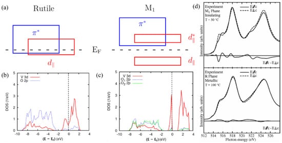
Figure 4. (a) Schematic band diagrams for VO2 in the metallic (rutile) phase and the semiconducting(monoclinic) phase. (b) Partial DOS of rutile VO2 as calculated using the HSE functional. (c) Partial DOS of M1-VO2 as calculated using the HSE (bottom) functional. (d) Experimental V L2;3 XAS spectra of VO2 in the insulating M1 phase (top panel, T = 30 °C) and the metallic R phase (bottom panel, T = 100 °C) taken with the light polarization E→//c
(solid lines) and E→⊥c
(dashed lines).
3.2. Properties of VO2 and Other Transition-Metal Oxide O-PCMs
VO2 is a promising reconfigurable and reprogrammable active optical PCM because of its distinctive insulator-to-metal phase transition. It provides orders of magnitude change in the resistivity and large changes in absorption and the refractive index, which is accessible in the range from near- to far-infrared wavelength [15].
At a critical temperature of TC = ≈67 °C (340 K), VO2 undergoes a significant and reversible insulator-to-metal phase transition in response to an increase in the temperature [16]. In the process of the phase transition, the structural transition occurs, with a change from a low-temperature monoclinic phase to a high-temperature rutile phase. The fundamental atomic structures of VO2 are shown in Figure 5 [14]. The insulator with a monoclinic structure is shown in Figure 5a, and its bandgap is about 0.7 eV. The metal with the rutile structure is shown in Figure 5b. The large and small spheres denote the metal and ligand atoms, respectively.
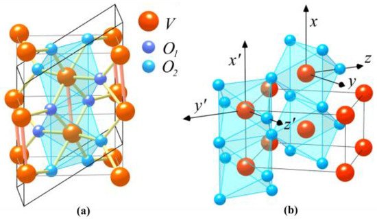
Figure 5. Crystal structures of (a) semiconducting(monoclinic) and (b) metallic (rutile) phases of VO2.
The phase transition of VO2 can also be induced by an applied terahertz electric field [17], hot-electron injection [18], strain [19], and all-optical pumping [20]. For all-optical pumping, the time of the phase transition is ~75 fs [21].
In the telecommunication wavelength bands near 1310 and 1550 nm, the changes of the real and imaginary parts of the refractive index of VO2 are obvious. At 1310 nm, the complex refractive index of VO2 changes from about 3.2 + 0.5i in the insulating phase to about 1.5 + 2.5i in the metallic phase. At 1550 nm, the complex refractive index of VO2 changes from about 2.9 + 0.4i in the insulating phase to about 2.0 + 3i in the metallic phase [22]. The wavelength dispersions of the refractive index (n) and extinction coefficient (k) of sputtered VO2 thin films in both states (semiconductor at T < TC and metal at T > TC) are shown in Figure 6 [23].
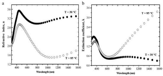
Figure 6. Wavelength dispersions of VO2 thin films. (a) Refractive index, n and (b) extinction coefficient, k. Thin films at temperatures below and above the phase transition temperature of 67 °C determined by UVISEL spectroscopic ellipsometry.
There are very large changes in the optical, dielectric, and electrical properties of materials when the transition occurs with thermal excitation [24]. The transition from the dielectric to the metallic state can be as fast as femtoseconds (“on”), while the transition from the metallic state back to the dielectric state is slower, with transition times ranging from ~1–10 ps (“off”).
VO2 has been incorporated into silicon photonics, plasmonics, and other hybrid nanocomposites to achieve improved performance, and it also provides platforms for reconfigurable photonics and enables the construction of ultrafast optical switches, modulators, and memory elements [15]. However, VO2 is unsuitable for nonvolatile and reconfigurable applications.
References
- Linjie Zhou; Hanyu Zhang; Hao Hu; Ningning Wang; Liangjun Lu; B. M. A. Rahman; Jianping Chen; Non-volatile silicon photonic devices enabled by phase change material. 2019 18th International Conference on Optical Communications and Networks (ICOCN) 2019, ., 1-3, 10.1109/icocn.2019.8934268.
- Mohammadreza Khorasaninejad; Wei Ting Chen; Robert C. Devlin; Jaewon Oh; Alexander Y. Zhu; Federico Capasso; Metalenses at visible wavelengths: Diffraction-limited focusing and subwavelength resolution imaging. Science 2016, 352, 1190-1194, 10.1126/science.aaf6644.
- Sanja Milošević; Ivana Stojković; Sandra Kurko; Jasmina Grbović Novaković; Nikola Cvjetićanin; The simple one-step solvothermal synthesis of nanostructurated VO2(B). Ceramics International 2012, 38, 2313-2317, 10.1016/j.ceramint.2011.11.001.
- M. Wuttig; H. Bhaskaran; Thomas Taubner; Phase-change materials for non-volatile photonic applications. Nature Photonics 2017, 11, 465-476, 10.1038/nphoton.2017.126.
- Alexander V. Kolobov; Paul Fons; Anatoly I. Frenkel; Alexei L. Ankudinov; Junji Tominaga; Tomoya Uruga; Understanding the phase-change mechanism of rewritable optical media. Nature Materials 2004, 3, 703-708, 10.1038/nmat1215.
- Lei Wang; Liang Tu; Jing Wen; Application of phase-change materials in memory taxonomy. Science and Technology of Advanced Materials 2017, 18, 406-429, 10.1080/14686996.2017.1332455.
- Noboru Yamada; Eiji Ohno; Nobuo Akahira; Ken'ichi Nishiuchi; Ken'ichi Nagata; Masatoshi Takao; High Speed Overwritable Phase Change Optical Disk Material. Japanese Journal of Applied Physics 1987, 26, 61-66, 10.7567/jjaps.26s4.61.
- Tun Cao; Rongzi Wang; Robert E. Simpson; Guixin Li; Photonic Ge-Sb-Te phase change metamaterials and their applications. Progress in Quantum Electronics 2020, 74, 100299, 10.1016/j.pquantelec.2020.100299.
- Lutz Waldecker; Timothy A. Miller; Miquel Rudé; Roman Bertoni; Johann Osmond; Valerio Pruneri; Robert E. Simpson; Ralph Ernstorfer; Simon Wall; Time-domain separation of optical properties from structural transitions in resonantly bonded materials. Nature Materials 2015, 14, 991-995, 10.1038/nmat4359.
- K E Goodson; Ordering up the minimum thermal conductivity of solids. Science 2007, 315, 342–343.
- J. Cao; W. Fan; K. Chen; N. Tamura; M. Kunz; V. Eyert; J. Wu; Constant threshold resistivity in the metal-insulator transition ofVO2. Physical Review B 2010, 82, 241101, 10.1103/physrevb.82.241101.
- Jae Hyung Park; Jim M. Coy; Talip Kasirga; Chunming Huang; Zaiyao Fei; Scott Hunter; David H. Cobden; Measurement of a solid-state triple point at the metal–insulator transition in VO2. Nature 2013, 500, 431-434, 10.1038/nature12425.
- V. Eyert; VO2: A Novel View from Band Theory. Physical Review Letters 2011, 107, 016401, 10.1103/physrevlett.107.016401.
- V. Eyert; The metal-insulator transitions of VO2: A band theoretical approach. Annalen der Physik 2002, 11, 650-704, 10.1002/1521-3889(200210)11:9<650::aid-andp650>3.0.co;2-k.
- Judson D. Ryckman; Kent A. Hallman; Robert E. Marvel; Richard F. Haglund; Sharon M. Weiss; Ultra-compact silicon photonic devices reconfigured by an optically induced semiconductor-to-metal transition. Optics Express 2013, 21, 10753-10763, 10.1364/oe.21.010753.
- C. N. Berglund; H. J. Guggenheim; Electronic Properties of VO2near the Semiconductor-Metal Transition. Physical Review 1969, 185, 1022-1033, 10.1103/physrev.185.1022.
- G Stefanovich; A Pergament; Electrical switching and Mott transition in VO2. Journal of Physics: Condensed Matter 2000, 12, 8837-8845, 10.1088/0953-8984/12/41/310.
- Masaki Hada; Dongfang Zhang; Albert Casandruc; R. J. Dwayne Miller; Yusaku Hontani; Jiro Matsuo; Robert E. Marvel; Richard F. Haglund; Hot electron injection driven phase transitions. Physical Review B 2012, 86, 13, 10.1103/physrevb.86.134101.
- J. Cao; E. Ertekin; V. Srinivasan; W. Fan; S. Huang; H. Zheng; J. W. L. Yim; D. R. Khanal; D. F. Ogletree; J. C. Grossman; et al.Junqiao Wu Strain engineering and one-dimensional organization of metal–insulator domains in single-crystal vanadium dioxide beams. Nature Nanotechnology 2009, 4, 732-737, 10.1038/nnano.2009.266.
- A. Cavalleri; Cs. Tóth; C. W. Siders; J. A. Squier; F. Ráksi; P. Forget; J. C. Kieffer; Femtosecond Structural Dynamics inVO2during an Ultrafast Solid-Solid Phase Transition. Physical Review Letters 2001, 87, 237401, 10.1103/physrevlett.87.237401.
- A. Cavalleri; Th. Dekorsy; H. H. W. Chong; J. C. Kieffer; R. W. Schoenlein; Evidence for a structurally-driven insulator-to-metal transition inVO2: A view from the ultrafast timescale. Physical Review B 2004, 70, 16, 10.1103/physrevb.70.161102.
- Joyce K. S. Poon; Arash Joushaghani; Junho Jeong; Suzanne Paradis; David Alain; Electrically controlled nanophotonic devices using the phase transition of vanadium dioxide. 2015 IEEE Summer Topicals Meeting Series (SUM) 2015, ., 217-218, 10.1109/phosst.2015.7248275.
- J.B. Kana Kana; J.M. Ndjaka; G. Vignaud; A. Gibaud; M. Maaza; Thermally tunable optical constants of vanadium dioxide thin films measured by spectroscopic ellipsometry. Optics Communications 2011, 284, 807-812, 10.1016/j.optcom.2010.10.009.
- Kevin J. Miller; Richard F. Haglund; Sharon M. Weiss; Optical phase change materials in integrated silicon photonic devices: review. Optical Materials Express 2018, 8, 2415-2429, 10.1364/ome.8.002415.
- Ana Simović; Alexandar Djordjevich; Svetislav Savović; Influence of depth of intermediate layer on optical power distribution in W-type optical fibers.. Applied Optics 2012, 51, 4896-4901, 10.1364/ao.51.004896.
More
Information
Subjects:
Others
Contributor
MDPI registered users' name will be linked to their SciProfiles pages. To register with us, please refer to https://encyclopedia.pub/register
:
View Times:
2.2K
Revision:
1 time
(View History)
Update Date:
19 May 2021
Table of Contents


Notice
You are not a member of the advisory board for this topic. If you want to update advisory board member profile, please contact office@encyclopedia.pub.
OK
Confirm
Only members of the Encyclopedia advisory board for this topic are allowed to note entries. Would you like to become an advisory board member of the Encyclopedia?
Yes
No
${ textCharacter }/${ maxCharacter }
Submit
Cancel
Back
Comments
${ item }
|
${ item.createdUser.fullName }
${ item.createdAt }
${ item.vote }
${ item.reply }
Delete
${ reply.createdUser.fullName }
${ reply.createdAt }
${ reply.vote }
Delete
There is no reply to this comment~
${ item.replyTextCharacter }/${ item.replyMaxCharacter }
Submit
Cancel
More
No more~
There is no comment~
${ textCharacter }/${ maxCharacter }
Submit
Cancel
${ selectedItem.replyTextCharacter }/${ selectedItem.replyMaxCharacter }
Submit
Cancel
Confirm
Are you sure to Delete?
Yes
No