 +1 credit
| Version | Summary | Created by | Modification | Content Size | Created at | Operation |
|---|---|---|---|---|---|---|
| 1 | Cesar Magen | + 2520 word(s) | 2520 | 2021-02-15 12:08:42 | | | |
| 2 | Vivi Li | Meta information modification | 2520 | 2021-03-04 10:04:48 | | |
Video Upload Options
Focused-electron-beam-induced deposition (FEBID) is the ultimate additive nanofabrication technique for the growth of 3D nanostructures. In the field of nanomagnetism and its technological applications, FEBID could be a viable solution to produce future high-density, low-power, fast nanoelectronic devices based on the domain wall conduit in 3D nanomagnets. While FEBID has demonstrated the flexibility to produce 3D nanostructures with almost any shape and geometry, the basic physical properties of these out-of-plane deposits are often seriously degraded from their bulk counterparts due to the presence of contaminants. 3D Co nanowires have been used to test the possibilities of FEBID for engineering the dimensions, composition and magnetism of these nanostructures.
1. Introduction
Three-dimensional (3D) magnetic nanostructures are the playground of a wide range of exciting physical phenomena in nanomagnetism, where curved geometries enable the onset of new types of exotic magnetic configurations, such as topologically protected and chiral magnetic textures [1][2][3][4]. Furthermore, 3D nanomagnets present several key features to postulate a paradigmatic solution to different challenges that the semiconductor industry must confront in the years to come to reconcile continued miniaturization, increasing performance and reduced power consumption [5][6][7]. The transition to 3D nanoarchitectures would overcome the intrinsic areal density limitations of conventional CMOS technologies caused by increasing leakage currents due to quantum effects [8]. They may also reduce the power consumption by storing and processing memory by ultrafast magnetic domain walls or skyrmions driven by low-power spin currents [9][10][11].
Even though the growth of high-purity, narrow 3D ferromagnetic structures may be the gateway to a broad range of opportunities for both fundamental and technological applications, most standard nanolithography techniques lack the flexibility to implement complex 3D structures at the nanoscale. For this purpose, additive manufacturing approaches to nanofabrication present an ideal solution. Among them, focused-electron-beam-induced deposition (FEBID) presents unique properties to become the ultimate 3D nano-printing technique [12]. FEBID is a single-step additive nanolithography technique based on the local decomposition of the molecules of an organometallic precursor gas, adsorbed on the surface of a substrate, thus producing a solid deposit [13][14]. This mechanism is mainly driven by the interaction of the primary beam and the secondary electrons emitted by the substrate with the adsorbed precursor molecules [15]. This basic principle confers a great control on the material deposit, geometry, and growth conditions to design conducting, insulating, superconducting, plasmonic or ferromagnetic structures, with virtually any shape and nanometer resolution, in 2D [16] and 3D [17]. Over the years, numerous types of FEBID deposits have been developed as structural materials [18], for electrical contacting [19], nanosensing [20] or plasmonic structures [21]. In particular, the growth of 3D ferromagnets by FEBID has been fruitful and yielded highly sophisticated architectures. Remarkable applications have been developed in magnetic sensing by functionalization of magnetic probes for magnetic force microscopy [22] and ferromagnetic resonance force microscopy [23] in materials science and biology [24], as magnetically driven mechanical nano-actuators [25], 3D domain wall conduit [26], ferromagnetic designs based on 3D FEBID scaffolds [18], arrays of 3D nanopillars for magnetic logic [27], 3D artificial ferromagnetic lattices [27][28], and magnetically chiral 3D architectures [29]. Further examples of applications of 3D FEBID ferromagnets have been reviewed recently by Fernández-Pacheco et al. [30].
One of the main difficulties of FEBID growth for the design of high-performance nanodevices is to obtain the desired geometry and dimensions with a high level of purity. The presence of a degree of contaminants in the deposit is inherent to the FEBID process, as some of the precursor residues are easily integrated into the deposit together with the active material [31], while secondary electrons emitted away from beam position induce the formation of an extended halo [32]. These drawbacks have motivated a dedicated effort for optimization of FEBID growth conditions, beginning with the choice of the gas precursor. Numerous precursor molecules have been explored for the growth of ferromagnetic materials. A detailed account of the precursors reported in the literature for 2D growth of ferromagnets is beyond the scope of this review, and has been reported elsewhere [33], but it is worth discussing some key aspects. Most of the precursors that have been reported are organometallic complexes based on carbonyl (CO) groups, thus C and O are the expected impurities derived from incomplete precursor decomposition. The most widely used is dicobalt octacarbonyl, Co2(CO)8, for which 2D deposits with 95 at. % Co content with metallic conduction have been achieved without further post-processing [34], even in halo-free extremely narrow (<30 nm) nanowires [35]. Co(CO)3NO has also been tested for 2D FEBID growth, and metal contents of 50–55 at. % have been obtained [36][37]. In the case of iron, the main precursors used are Fe(CO)5 [38] and Fe2(CO)9 [39], and metal contents above 75 at. % have been obtained. Iron precursors evidence the importance of residual gases in the deposition chamber, and 95 at. % purity can be achieved in ultra-high vacuum conditions with Fe(CO)5 [40]. The use of heteronuclear precursors allows one to grow alloyed magnetic materials; for instance, the precursor HCo3Fe(CO)12 has been used to produce Co3Fe deposits with metallic contents as high as 80 at. % [41], and has also been grown in 3D [28]. The nickel precursors reported are not carbonyl-based; FEBID deposits based on Ni(C5H4CH3)2 [42][43] or Ni(PF3)4 [42] do not surpass metal contents of 40 at. %. 3D growth of ferromagnets has been attempted with precursors that already provide high purity levels in 2D. In the present work, the precursors used are Co2(CO)8 for cobalt and Fe2(CO)9 for iron.
Furthermore, 3D growth implies substantial challenges with respect to 2D growth. As the deposit grows vertically, the geometry of the deposition area changes drastically, and the relevant electron beam interaction is now with the growing deposit, instead of the substrate. Many key parameters for the FEBID process are bound to change with respect to 2D, such as the interaction volume of the electron beam, secondary electron emission, precursor molecules adsorption and diffusion rates, and heat dissipation [44][45]. A deep understanding of these processes allows engineering the geometrical, compositional and magnetic properties of 3D ferromagnetic nanowires by FEBID.
2. Going 3D: Tuning FEBID Growth Parameters
While 3D FEBID growth has achieved a high degree of architectural complexity with the use of computer-aided design models [17], for the optimization of the physical properties of 3D ferromagnetic deposits, the simple benchmark design of a straight vertical nanowire has been used. For this type of geometry, the FEBID growth is performed in spot mode, where a stationary electron beam is focused into a single point of the substrate for a period of time. To facilitate a detailed, local characterization of the physical properties of the 3D deposits, these are grown out on the edge of a commercial TEM Cu grid.
The main growth parameters left are the primary beam energy, the beam current and the precursor gas flux. While the variation of the primary beam energy by itself does not significantly affect the composition, the interplay between the beam current and the precursor gas flux is essential to determine the final properties of the 3D nanowire. Indeed, two growth modes have been evidenced in Co FEBID nanowires, the so-called linear regime and the radial regime [46]. The transition between these two regimes is marked by a sudden change of the nanowire’s diameter, depending on the balance between the beam current and the precursor gas flux. The latter is parameterized through the working pressure, ΔP, defined as the increase of pressure with respect to the base pressure, caused by the precursor gas flux injected during growth. As shown in Figure 1a–d, for a given beam current of 86 pA, a high ΔP of 7.3 × 10⁻⁶ mbar produces long nanowires with a diameter well below 75 nm, while at low working pressure (ΔP = 5.1 × 10⁻⁶ mbar), shorter and thicker nanowires are grown, of about 120 nm in diameter. Intermediate values of ΔP give rise to hybrid objects, which evidence linear growth in the early stages up to a certain height, at which the growth transits into radial regime. It is worth noting that for higher beam currents, this transition occurs at higher working pressures, i.e., higher precursor gas fluxes. Thus, the growth rate is determined by the amount of gas molecules delivered (increasing with ΔP), which is known as the precursor-limited regime [47]. Consequently, the nanowires (or segments of nanowire) grown in the linear regime present a high growth rate, expressed in terms of nanowire’s length per unit of time, while in the radial regime, nanowires grow more slowly. The growth mode also reflects on the composition of the nanowire. The radial regime gives rise to the nanowires with the highest Co content, close to 90 at. % Co, while in the linear regime, the values decrease below 70 at. % Co. This tendency is observed even for nanowires that present both growth regimes. There is an illustrative example in Figure 1e, which represents the drastic change in Co content at the transition point between linear and radial regime, determined by electron energy loss spectroscopy (EELS) in scanning transmission electron microscopy (STEM).
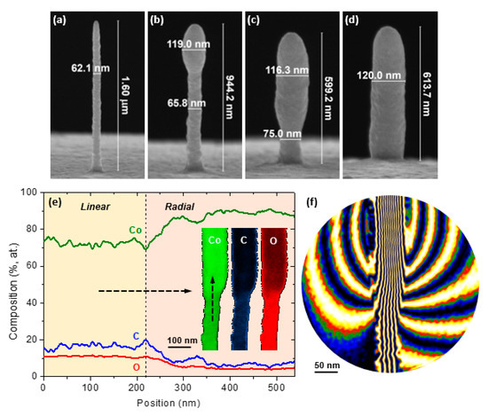
Figure 1. Growth modes of 3D Co focused-electron-beam-induced deposition (FEBID) nanowires. (a) Dependence of the transition from linear growth to radial growth with the working pressure increase due to gas injection, ΔP: (a) 7.3 × 10⁻⁶ mbar, (b) 6.4 × 10⁻⁶ mbar, (c) 5.9 × 10⁻⁶ mbar, (d) 5.1 × 10⁻⁶ mbar. (e) Compositional dependence with the growth mode, with STEM-EELS elemental maps in the inset, where Co, C and O are depicted in green, blue and red, respectively. The arrows indicate the direction of the elemental line profile. (f) Magnetic flux lines around the transition point between sections grown in radial regime (top) and linear regime (bottom). Adapted from Refs. [48][49].
The microscopic origin of this general behavior is evidently complex and requires careful theoretical simulation. However, some aspects can be qualitatively understood as a consequence of the more or less efficient thermal dissipation, and its impact on the gas precursor molecules adsorption/desorption and decomposition. Considering a nanowire growing in the threshold between the linear and radial regimes, at an early stage of growth, the tip of the nanowire is close to the substrate and the heat generated by the electron beam is easily dissipated onto the substrate. However, as the growth continues, the thermal resistance of the deposit increases, and heat is dissipated less efficiently [44]. At this point, the precursor gas may act as a heat-exchange medium. If the working pressure is high enough, thermal dissipation will be sufficient to maintain the linear growth. However, below a certain working pressure, the temperature at the growth point will increase, favoring a faster decomposition of the gas precursor molecules adsorbed and producing a wider deposit. This subtle balance between the heat produced by the electron probe and the capacity to dissipate it is supported by the fact that, at higher beam current (thus, higher temperature at the growth point), a higher precursor flux (thus, more efficient heat exchange) is required to operate in the linear regime. In terms of metallic content, high gas precursor flux favors an incomplete decomposition of the molecules, decreasing the metallic content of the deposit. As a consequence, high working pressure promotes the growth of narrow, though lower purity, 3D Co nanowires.
The beam current is another critical parameter to tailor the composition of 3D nanowires. Co content increases with the beam current, sharply at low currents, up to 80 at. % Co for 200 pA, and moderately at higher currents. As the beam current rises, the precursor molecules are decomposed more efficiently. This also favors the radial regime, as the amount of heat to be dissipated increases, and therefore, the diameters tend to be higher [48].
Of course, Co content of the 3D nanowires have a direct impact on the magnetism. This can be analyzed by off-axis electron holography, which is able to quantify the net magnetic induction of ferromagnetic materials [50]. Figure 1e illustrates qualitatively how the transition from radial to linear regime in a single nanowire causes a reduction of the magnetic flux lines density, which is associated to the lower magnetic induction (B) caused by the reduced Co content. Figure 2 represents the magnetic induction flux produced by 3D Co nanowires with different diameters. The widest nanowire is grown in the radial regime (Figure 2a) with a diameter of 124 nm and a composition of 87 at. % Co, and has an average magnetic induction of 1.33 T, which is 75% of the bulk value (Bbulk = 1.76 T). Our estimation does not take into account the fact that the outer surface of the 3D Co FEBID nanowires is oxidized due to air exposure, producing a non-ferromagnetic shell. This oxide layer is highlighted by colored bands in the outer regions where the magnetic induction decays (Figure 2d). The thinnest nanowire is grown in the linear mode (Figure 2c, 57 nm in diameter) and presents a very low magnetic induction of 0.41 T (23% of Bbulk), in accordance with a much poorer Co content of 41 at. %. This deposit has a much higher surface-to-volume ratio, so the relative contribution of the oxidized surface is remarkable and it is reasonable to think that the inner magnetic induction values are greatly underestimated. Finally, Figure 2b depicts the nanowire with intermediate thickness, grown in the range where radial and linear regimes coexist. This nanowire evidences values of all physical parameters halfway between the two extreme cases: with a diameter of 81 nm, the composition and magnetic induction values are 68 at. %. Co and 0.78 T (44% of Bbulk), respectively.
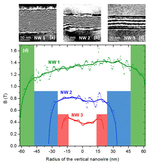
Figure 2. Magnetic properties of as-grown 3D Co FEBID nanowires. (a–c) Magnetic induction (B) flux maps of nanowires with diameters of 124, 81 and 57 nm, respectively. (d) Cross-sectional profiles of B, where the surface regions are marked with vertical color bands. Adapted from Ref. [48]
This study demonstrates that the variation of the main FEBID growth parameters enables the tailoring of the structural, compositional and magnetic properties of the 3D nanowires. They can even be modulated, as evidenced by the observed change in diameter and composition in a single nanowire at the transition from the linear regime segment to the radial regime one. This phenomenon could be exploited to engineer pinning of domain walls of exotic nature [51][52]. However, the key growth parameters and physical properties are mutually dependent, as the Co content, and thus the magnetism, are directly linked to the growth regime, which determines the average diameter and the growth rate. These interrelations are summarized in Figure 3, which represents the dependence of the Co content of nanowires grown in the optimal conditions for a given diameter, together with the net magnetic induction obtained for the three Co nanowires analyzed by electron holography. It is clear that both the composition and magnetic induction inevitably decrease with the reduction of the nanowire’s diameter, and the Co content never surpasses 70 at. % Co for diameters below 80 nm. According to the holography results, this would correspond to a magnetic induction of approximately 0.8 T, which could have a significant impact on the functionality of the nanowires.
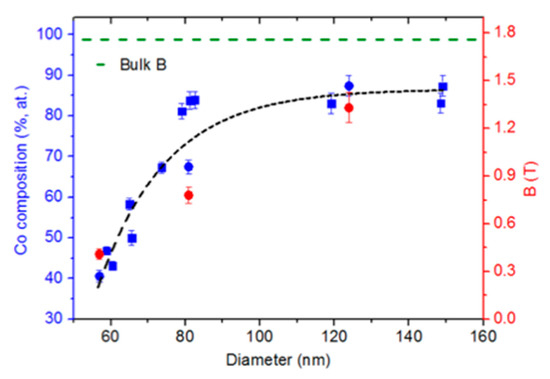
Figure 3. Composition (in blue) and net magnetic induction (in red) of 3D Co nanowires as a function of the diameter. Adapted from Ref. [48]
Therefore, to produce 3D Co nanowires with a high aspect ratio, diameters well below 100 nm and with good functional properties, namely a high (>90 at. %) Co content and a saturation magnetization close to the bulk value, tuning the basic growth parameters is not enough and post-growth purification procedures [53] or heterostructuring [49] are required.
References
- Amalio Fernández-Pacheco; Robert Streubel; Olivier Fruchart; Riccardo Hertel; Peter Fischer; Russell P. Cowburn; Three-dimensional nanomagnetism. Nature Communications 2017, 8, 15756, 10.1038/ncomms15756.
- Robert Streubel; Peter Fischer; Florian Kronast; Volodymyr P Kravchuk; Denis D Sheka; Yuri Gaididei; Oliver G Schmidt; Denys Makarov; Magnetism in curved geometries. Journal of Physics D: Applied Physics 2016, 49, 363001, 10.1088/0022-3727/49/36/363001.
- Michal Stano; Olivier Fruchart. Magnetic Nanowires and Nanotubes; Brück, E., Eds.; Elsevier: Amsterdam, The Netherlands, 2018; pp. 155-267.
- Eider Berganza; Miriam Jaafar; José Ángel Fernández-Roldán; Maite Goiriena-Goikoetxea; Javier Pablo-Navarro; Alfredo García-Arribas; Konstantin Guslienko; César Magén; Jose Maria De Teresa; Oksana Chubykalo-Fesenko; et al.Agustina Asenjo Half-hedgehog spin textures in sub-100 nm soft magnetic nanodots. Nanoscale 2020, 12, 18646–18653, 10.1039/d0nr02173c.
- Stuart S. P. Parkin; Masamitsu Hayashi; Luc Thomas; Magnetic Domain-Wall Racetrack Memory. Science 2008, 320, 190-194, 10.1126/science.1145799.
- Arne Brataas; Andrew D. Kent; Hideo Ohno; Current-induced torques in magnetic materials. Nature Materials 2012, 11, 372-381, 10.1038/nmat3311.
- Jorge Puebla; Junyeon Kim; Kouta Kondou; Yoshichika Otani; Spintronic devices for energy-efficient data storage and energy harvesting. Communications Materials 2020, 1, 1-9, 10.1038/s43246-020-0022-5.
- Henry H. Radamson; Huilong Zhu; Zhenhua Wu; Xiaobin He; Hongxiao Lin; Jinbiao Liu; Jinjuan Xiang; Zhenzhen Kong; Wenjuan Xiong; Junjie Li; et al.Hushan CuiJianfeng GaoHong YangYong DuBuqing XuBen LiXuewei ZhaoJiahan YuYan DongGuilei Wang State of the Art and Future Perspectives in Advanced CMOS Technology. Nanomaterials 2020, 10, 1555, 10.3390/nano10081555.
- R Hertel; Ultrafast domain wall dynamics in magnetic nanotubes and nanowires. Journal of Physics: Condensed Matter 2016, 28, 483002, 10.1088/0953-8984/28/48/483002.
- Ming Yan; Attila Kákay; Sebastian Gliga; Riccardo Hertel; Beating the Walker Limit with Massless Domain Walls in Cylindrical Nanowires. Physical Review Letters 2010, 104, 057201, 10.1103/physrevlett.104.057201.
- Albert Fert; Nicolas Reyren; Vincent Cros; Magnetic skyrmions: advances in physics and potential applications. Nature Reviews Materials 2017, 2, 17031, 10.1038/natrevmats.2017.31.
- Albert Fert; Nicolas Reyren; Vincent Cros; Magnetic skyrmions: advances in physics and potential applications. Nature Reviews Materials 2017, 2, 7031, 10.1038/natrevmats.2017.31.
- R. Winkler; J. D. Fowlkes; P. D. Rack; H. Plank; 3D nanoprinting via focused electron beams. Journal of Applied Physics 2019, 125, 210901, 10.1063/1.5092372.
- Ivo Utke; Patrik Hoffmann; John Melngailis; Gas-assisted focused electron beam and ion beam processing and fabrication. Journal of Vacuum Science & Technology B: Microelectronics and Nanometer Structures 2008, 26, 1197, 10.1116/1.2955728.
- W. F. Van Dorp; C. W. Hagen; A critical literature review of focused electron beam induced deposition. Journal of Applied Physics 2008, 104, 081301, 10.1063/1.2977587.
- J. D. Fowlkes; S. J. Randolph; P. D. Rack; Growth and simulation of high-aspect ratio nanopillars by primary and secondary electron-induced deposition. Journal of Vacuum Science & Technology B: Microelectronics and Nanometer Structures 2005, 23, 2825, 10.1116/1.2101732.
- Leon Van Kouwen; Aurelien Botman; Cornelis W. Hagen; Focused Electron-Beam-Induced Deposition of 3 nm Dots in a Scanning Electron Microscope. Nano Letters 2009, 9, 2149-2152, 10.1021/nl900717r.
- Jason D. Fowlkes; Robert Winkler; Brett B. Lewis; Michael G. Stanford; Harald Plank; Philip D. Rack; Simulation-Guided 3D Nanomanufacturing via Focused Electron Beam Induced Deposition. ACS Nano 2016, 10, 6163-6172, 10.1021/acsnano.6b02108.
- Dédalo Sanz-Hernández; Ruben F. Hamans; Johannes Osterrieth; Jung-Wei Liao; Luka Skoric; Jason D. Fowlkes; Philip D. Rack; Anna Lippert; Steven F. Lee; Reinoud Lavrijsen; et al.Amalio Fernández-Pacheco Fabrication of Scaffold-Based 3D Magnetic Nanowires for Domain Wall Applications. Nanomaterials 2018, 8, 483, 10.3390/nano8070483.
- T. Brintlinger; M. S. Fuhrer; J. Melngailis; I. Utke; T. Bret; A. Perentes; P. Hoffmann; M. Abourida; P. Doppelt; Electrodes for carbon nanotube devices by focused electron beam induced deposition of gold. Journal of Vacuum Science & Technology B: Microelectronics and Nanometer Structures 2005, 23, 3174, 10.1116/1.2130355.
- Harald Plank; Robert Winkler; Christian H. Schwalb; Johanna Hütner; Jason D. Fowlkes; Philip D. Rack; Ivo Utke; Michael Huth; Focused Electron Beam-Based 3D Nanoprinting for Scanning Probe Microscopy: A Review. Micromachines 2019, 11, 48, 10.3390/mi11010048.
- Robert Winkler; Franz-Philipp Schmidt; Ulrich Haselmann; Jason D. Fowlkes; Brett B. Lewis; Gerald Kothleitner; Philip D. Rack; Harald Plank; Direct-Write 3D Nanoprinting of Plasmonic Structures. ACS Applied Materials & Interfaces 2016, 9, 8233-8240, 10.1021/acsami.6b13062.
- Markus Stiller; José Barzola-Quiquia; Pablo D Esquinazi; Soraya Sangiao; José M De Teresa; Jan Meijer; Bernd Abel; Functionalized Akiyama tips for magnetic force microscopy measurements. Measurement Science and Technology 2017, 28, 125401, 10.1088/1361-6501/aa925e.
- Soraya Sangiao; César Magén; Darius Mofakhami; Grégoire De Loubens; José María De Teresa; Magnetic properties of optimized cobalt nanospheres grown by focused electron beam induced deposition (FEBID) on cantilever tips. Beilstein Journal of Nanotechnology 2017, 8, 2106-2115, 10.3762/bjnano.8.210.
- Miriam Jaafar; Javier Pablo-Navarro; Eider Berganza; Pablo Ares; César Magén; Aurélien Masseboeuf; Christophe Gatel; Etienne Snoeck; Julio Gómez-Herrero; José María De Teresa; et al.Agustina Asenjo Customized MFM probes based on magnetic nanorods. Nanoscale 2020, 12, 10090-10097, 10.1039/d0nr00322k.
- Paolo Vavassori; Matteo Pancaldi; Maria J. Perez-Roldan; Andrey Chuvilin; Andreas P Berger; Remote Magnetomechanical Nanoactuation. Small 2016, 12, 1013-1023, 10.1002/smll.201503351.
- Dédalo Sanz-Hernández; Ruben F. Hamans; Jung-Wei Liao; Alexander Welbourne; Reinoud Lavrijsen; Amalio Fernández-Pacheco; Fabrication, Detection, and Operation of a Three-Dimensional Nanomagnetic Conduit. ACS Nano 2017, 11, 11066-11073, 10.1021/acsnano.7b05105.
- Marco Gavagnin; Heinz D. Wanzenboeck; Stefan Wachter; Mostafa Moonir Shawrav; Anders Persson; Klas Gunnarsson; Peter Svedlindh; Michael Stöger-Pollach; Emmerich Bertagnolli; Free-Standing Magnetic Nanopillars for 3D Nanomagnet Logic. ACS Applied Materials & Interfaces 2014, 6, 20254-20260, 10.1021/am505785t.
- Lukas Keller; Mohanad K. I. Al Mamoori; Jonathan Pieper; Christian Gspan; Irina Stockem; Christian Schröder; Sven Barth; Robert Winkler; Harald Plank; Merlin Pohlit; et al.Jens MüllerMichael Huth Direct-write of free-form building blocks for artificial magnetic 3D lattices. Scientific Reports 2018, 8, 1-13, 10.1038/s41598-018-24431-x.
- Dédalo Sanz-Hernández; Aurelio Hierro-Rodriguez; Claire Donnelly; Javier Pablo-Navarro; Andrea Sorrentino; Eva Pereiro; César Magén; Stephen Mcvitie; José María De Teresa; Salvador Ferrer; et al.Peter FischerAmalio Fernández-Pacheco Artificial Double-Helix for Geometrical Control of Magnetic Chirality. ACS Nano 2020, 14, 8084-8092, 10.1021/acsnano.0c00720.
- Amalio Fernández-Pacheco; Luka Skoric; José María De Teresa; Javier Pablo-Navarro; Michael Huth; Oleksandr V. Dobrovolskiy; Writing 3D Nanomagnets Using Focused Electron Beams. Materials 2020, 13, 3774, 10.3390/ma13173774.
- A Botman; J J L Mulders; C W Hagen; Creating pure nanostructures from electron-beam-induced deposition using purification techniques: a technology perspective. Nanotechnology 2009, 20, 372001, 10.1088/0957-4484/20/37/372001.
- Georg Arnold; Rajendra Timilsina; Jason Fowlkes; Angelina Orthacker; Gerald Kothleitner; Philip D. Rack; Harald Plank; Fundamental Resolution Limits during Electron-Induced Direct-Write Synthesis. ACS Applied Materials & Interfaces 2014, 6, 7380-7387, 10.1021/am5008003.
- J M De Teresa; A Fernández-Pacheco; R Córdoba; L Serrano-Ramón; S Sangiao; M R Ibarra; Review of magnetic nanostructures grown by focused electron beam induced deposition (FEBID). Journal of Physics D: Applied Physics 2016, 49, 243003, 10.1088/0022-3727/49/24/243003.
- A Fernández-Pacheco; J M De Teresa; R Córdoba; M R Ibarra; Magnetotransport properties of high-quality cobalt nanowires grown by focused-electron-beam-induced deposition. Journal of Physics D: Applied Physics 2009, 42, 055005, 10.1088/0022-3727/42/5/055005.
- Luis Serrano-Ramón; Rosa Cordoba; Luis Alfredo Rodríguez; Cesar Magen; Etienne Snoeck; Christophe Gatel; Inés Serrano; Manuel Ricardo Ibarra; Jose Maria De Teresa; Ultrasmall Functional Ferromagnetic Nanostructures Grown by Focused Electron-Beam-Induced Deposition. ACS Nano 2011, 5, 7781-7787, 10.1021/nn201517r.
- Gian Carlo Gazzadi; Hans Mulders; Piet Trompenaars; Alberto Ghirri; Marco Affronte; Vincenzo Grillo; Stefano Frabboni; Focused Electron Beam Deposition of Nanowires from Cobalt Tricarbonyl Nitrosyl (Co(CO)3NO) Precursor. The Journal of Physical Chemistry C 2011, 115, 19606-19611, 10.1021/jp206562h.
- Samantha G. Rosenberg; Michael Barclay; D. Howard Fairbrother; Electron Beam Induced Reactions of Adsorbed Cobalt Tricarbonyl Nitrosyl (Co(CO)3NO) Molecules. The Journal of Physical Chemistry C 2013, 117, 16053-16064, 10.1021/jp404905t.
- M. Shimojo; M. Takeguchi; M. Tanaka; K. Mitsuishi; K. Furuya; Electron beam-induced deposition using iron carbonyl and the effects of heat treatment on nanostructure. Applied Physics A 2004, 79, 1869-1872, 10.1007/s00339-004-2952-z.
- R Lavrijsen; Rosa Córdoba; F J Schoenaker; T H Ellis; B Barcones; J T Kohlhepp; H J M Swagten; B Koopmans; J M De Teresa; C Magen; et al.M R IbarraP TrompenaarsJ J L Mulders Fe:O:C grown by focused-electron-beam-induced deposition: magnetic and electric properties. Nanotechnology 2010, 22, 025302, 10.1088/0957-4484/22/2/025302.
- Thomas Lukasczyk; Michael Schirmer; Hans-Peter Steinrück; Hubertus Marbach; Electron-Beam-Induced Deposition in Ultrahigh Vacuum: Lithographic Fabrication of Clean Iron Nanostructures. Small 2008, 4, 841-846, 10.1002/smll.200701095.
- F Porrati; M Pohlit; J Müller; S Barth; F Biegger; C Gspan; H Plank; M Huth; Direct writing of CoFe alloy nanostructures by focused electron beam induced deposition from a heteronuclear precursor. Nanotechnology 2015, 26, 475701-475701, 10.1088/0957-4484/26/47/475701.
- A. Perentes; G. Sinicco; Giovanni Boero; B. Dwir; P. Hoffmann; Focused electron beam induced deposition of nickel. Journal of Vacuum Science & Technology B: Microelectronics and Nanometer Structures 2007, 25, 2228, 10.1116/1.2794071.
- Rosa Córdoba; B Barcones; E Roelfsema; M A Verheijen; J J L Mulders; P H F Trompenaars; B Koopmans; Functional nickel-based deposits synthesized by focused beam induced processing. Nanotechnology 2016, 27, 065303, 10.1088/0957-4484/27/6/065303.
- Eva Mutunga; Robert Winkler; Jürgen Sattelkow; Philip D. Rack; Harald Plank; Jason Davidson Fowlkes; Impact of Electron-Beam Heating during 3D Nanoprinting. ACS Nano 2019, 13, 5198-5213, 10.1021/acsnano.8b09341.
- Luka Skoric; Dédalo Sanz-Hernández; Fanfan Meng; Claire Donnelly; Sara Merino-Aceituno; Amalio Fernández-Pacheco; Layer-by-Layer Growth of Complex-Shaped Three-Dimensional Nanostructures with Focused Electron Beams. Nano Letters 2019, 20, 184-191, 10.1021/acs.nanolett.9b03565.
- G. Hochleitner; H. D. Wanzenboeck; E. Bertagnolli; Electron beam induced deposition of iron nanostructures. Journal of Vacuum Science & Technology B: Microelectronics and Nanometer Structures 2008, 26, 939, 10.1116/1.2907781.
- Stefan Wachter; Marco Gavagnin; Heinz D. Wanzenboeck; Mostafa M. Shawrav; Domagoj Belić; Emmerich Bertagnolli; Nitrogen as a carrier gas for regime control in focused electron beam induced deposition. Nanofabrication 2014, 1, 16-22, 10.2478/nanofab-2014-0002.
- Javier Pablo-Navarro; Dédalo Sanz-Hernández; César Magén; Amalio Fernández-Pacheco; José María De Teresa; Tuning shape, composition and magnetization of 3D cobalt nanowires grown by focused electron beam induced deposition (FEBID). Journal of Physics D: Applied Physics 2017, 50, 18LT01, 10.1088/1361-6463/aa63b4.
- Javier Pablo-Navarro; César Magén; José María De Teresa; Three-dimensional core–shell ferromagnetic nanowires grown by focused electron beam induced deposition. Nanotechnology 2016, 27, 285302, 10.1088/0957-4484/27/28/285302.
- Lorena Marín; Luis A. Rodriguez; Cesar Magen; Etienne Snoeck; Rémi Arras; Irene Lucas; Luis Morellón; Pedro A. Algarabel; José M. De Teresa; M. Ricardo Ibarra; et al. Observation of the Strain Induced Magnetic Phase Segregation in Manganite Thin Films. Nano Letters 2014, 15, 492-497, 10.1021/nl503834b.
- Yurii P. Ivanov; Andrey Chuvilin; Sergei Lopatin; Jurgen Kosel; Modulated Magnetic Nanowires for Controlling Domain Wall Motion: Toward 3D Magnetic Memories. ACS Nano 2016, 10, 5326-5332, 10.1021/acsnano.6b01337.
- Jose Angel Fernandez-Roldan; Rafael Perez Del Real; Cristina Bran; Manuel Vazquez; Oksana Chubykalo-Fesenko; Magnetization pinning in modulated nanowires: from topological protection to the “corkscrew” mechanism. Nanoscale 2018, 10, 5923-5927, 10.1039/c8nr00024g.
- Albert Fert; Nicolas Reyren; Vincent Cros; Magnetic skyrmions: advances in physics and potential applications. Nature Reviews Materials 2017, 2, 17031, 10.1038/natrevmats.2017.31.

