Your browser does not fully support modern features. Please upgrade for a smoother experience.
Submitted Successfully!
 +1 credit
Thank you for your contribution! You can also upload a video entry or images related to this topic.
For video creation, please contact our Academic Video Service.
| Version | Summary | Created by | Modification | Content Size | Created at | Operation |
|---|---|---|---|---|---|---|
| 1 | Chin-An Ku | -- | 2560 | 2024-01-17 09:34:32 | | | |
| 2 | Lindsay Dong | + 6 word(s) | 2566 | 2024-01-19 02:41:41 | | | | |
| 3 | Lindsay Dong | Meta information modification | 2566 | 2024-01-22 02:55:46 | | | | |
| 4 | Lindsay Dong | + 2 word(s) | 2568 | 2024-01-22 02:56:23 | | |
Video Upload Options
We provide professional Academic Video Service to translate complex research into visually appealing presentations. Would you like to try it?
Cite
If you have any further questions, please contact Encyclopedia Editorial Office.
Ku, C.; Yu, C.; Hung, C.; Chung, C. Applications of Nanoporous Anodic Aluminum Oxide in Sensors. Encyclopedia. Available online: https://encyclopedia.pub/entry/53954 (accessed on 28 July 2026).
Ku C, Yu C, Hung C, Chung C. Applications of Nanoporous Anodic Aluminum Oxide in Sensors. Encyclopedia. Available at: https://encyclopedia.pub/entry/53954. Accessed July 28, 2026.
Ku, Chin-An, Chung-Yu Yu, Chia-Wei Hung, Chen-Kuei Chung. "Applications of Nanoporous Anodic Aluminum Oxide in Sensors" Encyclopedia, https://encyclopedia.pub/entry/53954 (accessed July 28, 2026).
Ku, C., Yu, C., Hung, C., & Chung, C. (2024, January 17). Applications of Nanoporous Anodic Aluminum Oxide in Sensors. In Encyclopedia. https://encyclopedia.pub/entry/53954
Ku, Chin-An, et al. "Applications of Nanoporous Anodic Aluminum Oxide in Sensors." Encyclopedia. Web. 17 January, 2024.
Copy Citation
Nanoporous anodic aluminum oxide (AAO) is an important template for 1D nanomaterial synthesis. It is used as an etching template for nanopattern transfer in a variety of contexts, including nanostructured material synthesis, electrical sensors, optical sensors, photonic and electronic devices, photocatalysis, and hardness and anticorrosion improvement.
anodic aluminum oxide
AAO
sensor
1. Nanoporous AAO and its Applications
Anodic aluminum oxide (AAO) technology is one of the most well-known technologies for the fabrication of nanostructured templates in industry and scientific research. Compared with other nanomaterial templates, AAO exhibits the advantages of nanoscale pores, self-organization, tunable nanostructures, and good physical and chemical stability [1]. Further, aluminum is one of the most famously used metals in industry, which makes aluminum surface treatments highly compatible with production lines. These characteristics make AAO an object for extensive research. AAO is categorized into a barrier type and porous type, according to its structure. The barrier type of AAO, with a thin and compact structure, was largely used in the past for protection and dielectric capacitors [2]. By contrast, the porous type of AAO, with a highly ordered nanopore arrangement, has received increasing attention as a template for fabricating nanowires or synthesizing other 1D/2D nanostructures [2][3][4][5][6], and as a nanopattern transfer for micro/nano applications, for instance, in the triboelectric nanogenerator (TENG) field [7][8]. AAO, as a nanomaterial template, is fabricated using certain electrochemical processes. Figure 1 provides an overview of the anodization parameters with the dependent pore geometry and morphology of AAO, including the pore diameter (Dp), interpore distance (Dint), pore wall thickness (w), barrier thickness (tb), and AAO thickness (t). The fabrication parameters during this process are concerned with the formation of AAO’s geometry and profile, which are linked to various applications. AAO’s pore geometry and morphology are mainly affected by the purity, voltage and voltage mold, reaction temperature, electrolyte content and concentration, and time. Impurities in the Al substrate will increase the dissolution, which causes an irregular pore structure with a non-obvious hexagonal structure. The anodization voltage is proportional to the Dint, with a positive relation to the Dp. The proper anodization voltage required for AAO formation is dependent on the electrolyte type and concentration. Modulations in AAO’s structure occur through complex interactions, which will directly affect the application performance. The voltage mold of the AAO fabrication process is shown in Figure 2. Generally speaking, the production of AAO includes polishing and different parameter-controlled anodization processes to meet the required nanostructure. In the detailed electrochemical anodization at a certain electrolyte content, the parameters can be modulated, including the temperature (low temperature vs. high temperature), voltage (mild anodization (MA) vs. hard anodization (HA)), waveforms of direct current anodization (DCA, Figure 2a), pulse anodization (PA, Figure 2b), reverse pulse anodization (Figure 2c), and hybrid pulse anodization (HPA, Figure 2d), for the desired pore structure and a more efficient process [9][10][11][12][13][14][15][16][17][18]. Figure 3 shows the various schematic AAO profiles that can be modulated by different processes or voltage molds. The AAO fabrication process can be divided into three categories [19][20]. The first is the most well-known process of fabricating AAO on bulk Al; this is presently the most useful method for preparing AAO. The special structure of bamboo [21][22] and branch structure [23][24] are also fabricated from bulk Al using the MA and HA modulation methods. The second is the pretextured stamp nanoimprinting method, which involves making a master stamp with a nanostructure to transfer concaves on an aluminum substrate, which is then followed by anodization for regular pores. The last is conducted by sputtering the Al film onto a substrate, e.g., Si; this method can integrate AAO with different substrates for further applications.
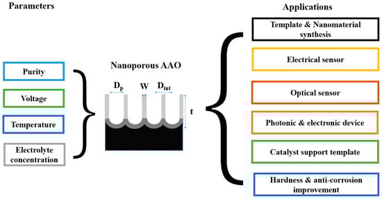
Figure 1. The anodization parameters and pore geometry overview of AAO and its applications. The interactive effects of parameters, profiles, and applications influence one another.
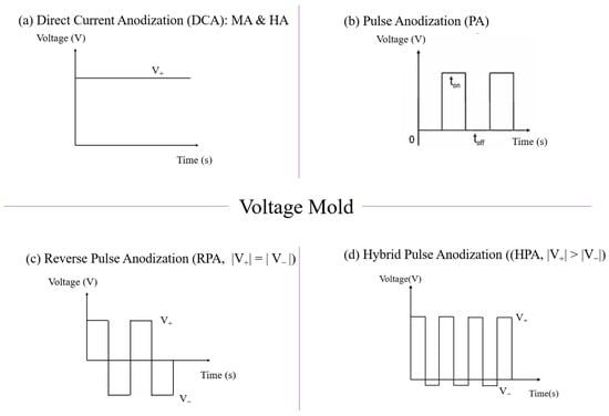
Figure 2. The voltage mold of AAO fabrication processes by different methods: (a) direct current anodization (DCA), (b) pulse anodization (PA) by a positive voltage and followed by 0 voltage, (c) reverse pulse anodization by a positive voltage and followed by the same value of negative voltage, and (d) hybrid pulse anodization (HPA) by a positive voltage and followed by a relatively small negative voltage.
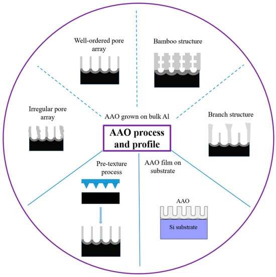
Figure 3. AAO process and profile control. AAO fabrication process can be divided into three categories: AAO grown on bulk Al, pretexture process, and AAO film on substrate.
2. Sensor Applications
AAO-based sensor applications can be divided into two categories: electrical sensors and optical sensors. The electrical AAO-based sensor is primarily based on two types of capacitance and resistance; usually, a thin metal film is deposited on the surface of AAO as an electrode for humidity [25][26] and gas [27] measurement. Many more publications on pure AAO humidity sensors than gas ones are probably attributed to the high response in sensing humidity.
2.1. Electrical Sensors
With the development of micro–nano technology and automated industry, sensor applications have received attention. Humidity sensors play a vital role in industrial development and daily life, encompassing fields such as weather forecasting, agriculture, process control, and materials or food preservation. AAO is one of the most famous ceramic nanomaterial templates with physical and chemical stability. After depositing a thin film of metal on AAO, the capacitor or resistor structure is formed and easy to apply for humidity measurement. This approach has garnered significant research attention in exploring sensor characteristics. Furthermore, the application of AAO humidity sensors involves measurements within a specific area (mm2), where the correlation with individual pore characteristics is not prominent. This characteristic allows the process of humidity sensors to be suitable for the one-step AAO fabrication process, which can replace the traditional two-step, low-temperature method.
In terms of the indicators of humidity sensors, two important characteristics are highlighted. One is the sensor’s response or sensitivity, which signifies its capability to differentiate between different humidity levels. In the context of AAO humidity sensors, this is often measured through capacitance, which can be defined as follows:
where ΔC is the capacitance change and C0 is the initial capacitance value of low humidity. Secondly, the response and recovery time indicates the measurement speed and the sensor’s ability to adapt to rapid environmental changes.
The sensing mechanism of AAO humidity sensors can be categorized into three main factors: external conditions, nanostructures [28][29][30], and anionic effect [28][31][32][33]. External conditions primarily involve changes in humidity and the application of an external magnetic field [31][32]. The capacitance calculation and the well-known adsorption theory were introduced by Nahar et al. [25][34]. When the humidity is below 45%, water vapor only forms a chemisorbed layer on the surface, resulting in a lower sensor response. On the other hand, when humidity is above 45%, a physically adsorbed layer is formed and the layering of these physical adsorbed layers causes the capacitance value to rapidly increase [25], exhibiting a natural function curve.
In terms of geometrical effect, Kashi et al. [28] studied the sensitivity of AAO by anodizing in phosphoric acid at high voltages of 165–185 V and enlarging the pore size to 107–127 nm. This study aimed to decrease the pore density of AAO while achieving better sensitivity. The improved AAO sensitivity was found to be related to the pore size (Dp) and anodization voltage. Additionally, the number of pores also plays a crucial role. Chung et al. [29] demonstrated that AAO produced from two-step anodization of high-purity aluminum at lower voltages possesses a larger total adsorption area, which can enhance the performance of AAO humidity sensors. A greater total adsorption area can absorb more water, thereby enhancing sensor response. Furthermore, humidity sensors based on AAO typically utilize the traditional two-step anodization process on small areas (<3 cm2) of high-purity aluminum (>99.99%) substrates at low temperatures (0–15 °C). However, this often leads to a lower response [35][36][37] and longer response–recovery time [26][38][39]. Non-AAO humidity sensors employing nanofibers, polyaniline (PANI), polyvinyl alcohol (PVA) [40], or nickel sulfide [41] have also been reported, but they also suffer from low strength and extended response–recovery times.
Table 1 lists a performance comparison between AAO-based humidity sensors [25][26][30][31][33][35][36][37][38] and some non-AAO sensors [40][41]. The traditional AAO humidity sensors are synthesized by two-step anodization from high-purity aluminum at low temperature or by the sputtering method. However, AAO humidity sensors have the potential to shorten the process through one-step anodization.
Table 1. Comparison of humidity sensor fabrication and performance.
| Reference | Fabrication Method/Time | Signal Intensity (RH%) |
Response (ΔC/C0) |
Response–Recovery Time |
|---|---|---|---|---|
| [25] | AAO/NA | 0.08–20 nF (RH5%–95%) |
About 20,000% | NA |
| [31] | AAO prepared by oxalic acid from high-purity Al/4 h | 0.65–108.9 nF (RH15%–80%) | 16,650% | NA |
| [33] | AAO prepared by oxalic acid from high-purity Al at −5 °C/NA | 1.5–60 nF (RH5%–95%) |
About 3900% | NA |
| [35] | AAO prepared by oxalic acid and pore widening from high-purity Al/6 h | 1.8–16 nF (RH5%–75%) |
793.02% | NA |
| [36] | Al sputtering on paper and anodized by phosphoric acid from high-purity Al/NA | NA (RH20%–80%) |
About 500% | NA |
| [37] | Spin coating polymer material on AAO/NA | 10–38 pF (RH20%–90%) |
280% | NA |
| [38] | Sputtered Al for AAO on Si from high-purity Al/NA | 2.08–2.17 pF (RH30%–90%) | About 4.4% | 289 s/286 s |
| [26] | AAO prepared by oxalic acid and pore widening from high-purity Al at 15 °C/8 h | NA | About 4830% | 18–188 s/NA |
| [39] | Silica and poly(3,4-ethylenedioxythiophene) composites/NA | About 20–1000 pF (RH11%–95%) |
About 4000% | 77 s/30 s |
| [40] | carbon nanofiber (CNF) and nanofibrillated cellulose (NFC)/27 h | About 231-3290 pF (RH40%- 100%) | About 100% | 41 s/50 s |
| [41] | bis(4-benzylpiperazine-1-carbodithioato-k2S, S′)nickel(II) complex/NA | 15.95 pF–38.1 pF (RH30%–90%) | About 138% | 25 s/30 s |
| [30] | AAO prepared by oxalic acid/2 h | 19.25–984.26 nF (RH20%–80%) |
5013% | Below 10 s/10 s |
2.2. Optical Sensors
Optical sensors are devices that transform the interaction between substrates and analytes into an optical signal, which is a technique that has been widely applied in chemical trace detection with label-free, fast, and non-invasive advantages. Common signal conversion technologies in optical sensors include reflection interference spectroscopy (RFIS) [42][43][44][45], photoluminescence spectroscopy (PL) [46][47][48][49], surface plasmon resonance (SPR) [50][51][52][53][54], and SERS [55][56][57][58][59][60][61]. AAO is an outstanding substrate for various optical sensing devices with the advantages of nanoscale pores, self-assembly properties, controllable geometry, and good biocompatibility. The optical sensors based on AAO substrates are described in the following sections and summarized in Table 2 with four different mechanisms: RIFS, PL, SPR, and SERS.
Table 2. Comparison of recent optical sensors based on AAO with the mechanisms of RIfS, PL, SPR, and SERS.
| Ref. | Technique | Analyte | LOD | Substrate |
|---|---|---|---|---|
| [42] | RIfS | Plant hormones (ABA, SA, auxins, cytokinins, gibberellins) | 0.1 μm | One-step vertical AAO on ITO glass chip |
| [43] | Quercetin | 0.14 mg/mL | Two-step bilayered or funnel-like NAA structures | |
| [44] | Cu2+ | 0.007 ppm | Two-step vertical AAO | |
| [45] | Drug release | - | One-step bamboo-like AAO fabricated by Sinusoidal anodization | |
| [48] | PL | Staphylococcus aureus Cocaine | 0.5 μm | Two-step vertical AAO |
| [49] | Vascular endothelial growth factor (VEGF) | 1 ng/μL | Two-step vertical AAO filled with ZnO | |
| [50] | SPR/LSPR | Label-free DNA | 5 nm | Nanobowled AAO barrier |
| [51] | Transmembrane protein CD63 | 1 ng/mL | Gold nano array fabricated using 2-step vertical AAO as a mask | |
| [52] | IgA | 10 ng/μL | Gold-capped 2-step vertical AAO | |
| [53] | Label-free DNA | 10 nM | Gold nanoantenna array fabricated using 1-step vertical AAO as a mask | |
| [54] | Cell interleukin-6 | 10 ng/mL | Nanoimprinting cyclo-olefin polymer (COP) using 2-step vertical AAO mold | |
| [55] | SERS | Aflatoxin B1 | 0.5 μg/L | Bipyramid-like nanoparticles in 2-step vertical AAO |
| [56] | C-reactive protein, interleukin-6, serum amyloid A, and procalcitonin | 53.4, 4.72, 48.3, and 7.53 fg/mL | Gold–Silver core–shell nanoparticles on commercial AAO | |
| [57] | Nitrate ion | 1.03 ppm | Gold nanoparticle clusters on 1-step AAO layer | |
| [58] | Methylene blue | - | UV-curable resin nanorod arrays using the 2-step branched AAO as a mold | |
| [62] | Beta-hydroxybutyric acid | 11 nM | Striped Au-Ag nanowire fabricated using vertical AAO as a shadow mask | |
| [59] | Rhodamine B | 1 × 10⁻¹⁰ mol/L | Ag-loaded bamboo-like AAO as 1D photonic crystal and defective photonic crystals | |
| [60] | Methylene blue | 1 nM | Irregular 1-step AAO pores | |
| [61] | Melamine | 0.05 ppm | Irregular 1-step AAO pores in 1–2 μm cavities |
RIfS is a useful optical method for sensing the substances, especially biomolecules, which is caused by the interference of light reflected from the top and bottom of the film [46]. The interference spectroscopy depends on the effective optical thickness (EOT), which can be calculated by the equation below:
EOT = 2 neff d cosθ = mλ
where EOT is the effective optical thickness, neff is the effective refractive index of AAO, d is the thickness of the AAO, m is the order of the interference, and λ is the wavelength of the light. After adding the analyte on the AAO film, a change in the EOT causes a shift of the interference spectroscopy. In general, to increase the sensitivity and selectivity of the measurement, the binding reaction between the analyte and the film is essential [46]. The nanostructured porous films compared with the planar polymer films have higher surface area for increasing the sensitivity [47].
Recently, Feng et al. presented an AAO-based RIFS biosensor to detect the different plant hormones including ABA, SA, auxins, cytokinins, and gibberellins by coating an aptamer on the AAO nanofilm [42]. Nemati et al. presented bilayered AAO films with hierarchical funnel-like structures for optimizing the optical sensing performance toward multi-analyte biosensing [43]. Kaur et al. combined self-assembled glutaraldehyde-cross-linked, double-layered, polyethylenimine (PEI-GA-PEI)-modified AAO interferometers and reflectometric interference spectroscopy (RIfS) as an optical sensing system for detecting ionic copper in environmental waters [44]. Kapruwan et al. exploited the optical properties of AAO gradient index filters, which have been used to measure the release dynamics of the cargo molecule in real time [45]. PL refers to light emission after the absorption of photons, which causes photon excitation and produces the electronic transition. The absorbed light causes the electrons of the material to jump to a higher state and then return back to a lower energy level with a light emission [47].
Surface plasmon resonance (SPR) is the oscillation of electrons on a metallic surface stimulated by an extra incident light. The analyte is detected based on the changes in the absorbance of SPR of the substrate [50]. Furthermore, AAO can be used to fabricate some nanostructure to produce localized surface plasmon resonance (LSPR). Compared with SPR, LSPR is more easily excited, which means complex optical configurations are unnecessary. Thus, some LSPR sensing researches using simple, even portable, optical devices have been reported [50][51][52][53][54].
Recently, SERS has been the most-published topic and can be applied for trace detection of various substances. SERS is a sensitive technique for detecting trace substances in industry, environment, wastewater, and air pollution. The enhancement comes from the overall effect of the electromagnetic mechanism (EM) and the chemical mechanism (CM). The EM is attributed to the local electrical field enhanced by the plasma resonance, and the CM is attributed to the electrons transfer between the analyte and the SERS substrate [60]. Here, the SERS substrates majorly based on the EM are discussed because the enhancement of EM is substantially higher than that of CM. The porous materials with properties of simple manufacturing and high aspect ratio are regarded as good candidates for forming the nanostructures of SERS substrates. Therefore, AAO with tunable nanopores is a popular material for fabricating the SERS substrate with various approaches. The current reported AAO-based SERS substrates can be divided into MNPs in the AAO pores [55][56][57], using AAO as a mold for fabricating the metal nanostructure array, and the metal film on the nanopores. First, AAO can be the support for the nanoparticles: Lin et al. used a drop-dry approach to deposit gold nanobipyramids (Au NBPs) into vertical two-step AAO pores as the SERS substrate to detect Aflatoxin B1. For Aflatoxin B1 sensing, the Au NBPs–AAO substrate has a corresponding linear range from 1.5 μg/L to 1.5 mg/L and an LOD of 0.5 μg/L [55].
Second, AAO can be the mold or the mask to fabricate the nanoparticles, nanowires, and nanorods. Chung et al. demonstrated the UV-curable resin nanorods array deposited with Ag MNPs as the SERS substrate. The UV-curable resin was filled into the nanopores of the two-step vertical and branched AAO to transfer the morphology of the nanopores to the UV-curable resin and generate the nanorods array.
References
- Wei, Q.L.; Fu, Y.Q.; Zhang, G.X.; Yang, D.C.; Meng, G.W.; Sun, S.H. Rational design of novel nanostructured arrays based on porous AAO templates for electrochemical energy storage and conversion. Nano Energy 2019, 55, 234–259.
- Diggle, J.W.; Downie, T.C.; Goulding, C.W. Anodic oxide films on aluminum. Chem. Rev. 1969, 69, 365–405.
- Zhang, C.; Liu, Z.; Li, C.; Cao, J.; Buijnsters, J.G. Templated Synthesis of Diamond Nanopillar Arrays Using Porous Anodic Aluminium Oxide (AAO) Membranes. Nanomaterials 2023, 13, 888.
- Wang, X.; Du, L.; Cheng, L.; Zhai, S.; Zhang, C.; Wang, W.; Lei, G. Pd/Ni nanowire film coated SAW hydrogen sensor with fast response. Sens. Actuators B Chem. 2022, 351, 130952.
- Zhang, H.; Zhou, M.; Zhao, H.; Lei, Y. Ordered nanostructures arrays fabricated by anodic aluminum oxide (AAO) template-directed methods for energy conversion. Nanotechnology 2021, 32, 502006.
- Zhi-Hua, L.; Yu-Xia, W.; Dan, Q.; Zai-Jun, L.; Zhi-Guo, G. AAO Assisted 1D Confined Assembly and 2D Surface Filming of Irone Triazole Nanomaterial and Spin-Crossover Properties. Chin. J. Inorg. Chem. 2017, 33, 2311–2321.
- Yoo, D.; Lee, S.; Lee, J.W.; Lee, K.; Go, E.Y.; Hwang, W.; Song, I.; Cho, S.B.; Kim, D.W.; Choi, D.; et al. Reliable DC voltage generation based on the enhanced performance triboelectric nanogenerator fabricated by nanoimprinting-poling process and an optimized high efficiency integrated circuit. Nano Energy 2020, 69, 104388.
- Lin, L.; Chung, C.-K. PDMS Microfabrication and Design for Microfluidics and Sustainable Energy Application: Review. Micromachines 2021, 12, 1350.
- Kim, S.W.; Lee, J.S.; Lee, S.W.; Kang, B.H.; Kwon, J.B.; Kim, O.S.; Kim, J.S.; Kim, E.S.; Kwon, D.H.; Kang, S.W. Easy-to-fabricate and high-sensitivity LSPR type specific protein detection sensor using AAO nano-pore size control. Sensors 2017, 17, 856.
- Norek, M.; Dopierała, M.; Bojar, Z. The influence of pre-anodization voltage on pore arrangement in anodic alumina produced by hard anodization. Mater. Lett. 2016, 183, 5–8.
- Manzano, C.V.; Rodríguez-Acevedo, J.; Caballero-Calero, O.; Martín-González, M. Interconnected three-dimensional anodized aluminum oxide (3D-AAO) metamaterials using different waveforms and metal layers for RGB display technology applications. J. Mater. Chem. C 2022, 10, 1787–1797.
- Woo, L.; Cheon, K.J. Highly ordered porous alumina with tailor-made pore structures fabricated by pulse anodization. Nanotechnology 2010, 21, 485304.
- Cigane, U.; Palevicius, A.; Jurenas, V.; Pilkauskas, K.; Janusas, G. Development and Analysis of Electrochemical Reactor with Vibrating Functional Element for AAO Nanoporous Membranes Fabrication. Sensors 2022, 22, 8856.
- Manzoor, S.; Tayyaba, S.; Ashraf, M.W. Simulation, analysis, fabrication and characterization of tunable AAO membrane for microfluidic filtration. J. Intell. Fuzzy Syst. 2022, 43, 2099–2108.
- Li, S.; Li, Y.; Jin, S.; Wu, J.; Li, Z.; Hu, X.; Ling, Z. Fabrication of crystallized porous anodic aluminum oxide under ultra-high anodization voltage. J. Electrochem. Soc. 2018, 165, E623.
- Guo, F.; Cao, Y.; Wang, K.; Zhang, P.; Cui, Y.; Hu, Z.; Xie, Z. Effect of the anodizing temperature on microstructure and tribological properties of 6061 aluminum alloy anodic oxide films. Coatings 2022, 12, 314.
- Chelliah, N.M.; Saxena, A.; Sharma, K.; Singh, H.; Surappa, M.K. Surface characterization of nanoporous aluminium oxide films synthesized by single-step DC and AC anodization. Surf. Interfaces 2017, 7, 139–145.
- Sulka, G.D.; Stepniowski, W.J. Structural features of self-organized nanopore arrays formed by anodization of aluminum in oxalic acid at relatively high temperatures. Electrochim. Acta 2009, 54, 3683–3691.
- Sulka, G.D. Introduction to anodization of metals. In Nanostructured Anodic Metal Oxides; Elsevier: Amsterdam, The Netherlands, 2020; pp. 1–34.
- Domagalski, J.T.; XifrePerez, E.; Marsal, L.F. Recent advances in nanoporous anodic alumina: Principles, engineering, and applications. Nanomaterials 2021, 11, 430.
- Lee, W.; Ji, R.; Gösele, U.; Nielsch, K. Fast fabrication of long-range ordered porous alumina membranes by hard anodization. Nat. Mater. 2006, 5, 741.
- Tu, Y.H.; Liu, C.T.; Chu, C.W.; He, H.C.; Chang, C.W.; Chen, J.T. Bamboo-like nanostructures prepared using template-based wetting methods: Molecular arrangements of polyimide and carbon tubes in cylindrical nanopores. Polymer 2019, 185, 121979.
- Blaszczyk-Lezak, I.; Juanes, B.D.; Martín, J.; Mijangos, C. Gecko-like Branched Polymeric Nanostructures from Nanoporous Templates. Langmuir 2018, 34, 11449–11453.
- Kim, B.; Lee, J.S. Formation of Anodic Aluminum Oxide with Branched and Meshed Pores. J. Nanosci. Nanotechnol. 2016, 16, 6575–6579.
- Nahar, R.K. Study of the performance degradation of thin film aluminum oxide sensor at high humidity. Sens. Actuators B Chem. 2000, 63, 49–54.
- Kim, Y.; Jung, B.; Lee, H.; Kim, H.; Lee, K.; Park, H. Capacitive humidity sensor design based on anodic aluminum oxide. Sens. Actuators B Chem. 2009, 141, 441–446.
- Podgolin, S.K.; Petukhov, D.I.; Dorofeev, S.G.; Eliseev, A.A. Anodic alumina membrane capacitive sensors for detection of vapors. Talanta 2020, 219, 121248.
- Kashi, M.A.; Ramazani, A.; Abbasian, H.; Khayyatian, A. Capacitive humidity sensors based on large diameter porous alumina prepared by high current anodization. Sens. Actuators A Phys. 2012, 174, 69–74.
- Chung, C.K.; Khor, O.K.; Kuo, E.H.; Ku, C.A. Total effective surface area principle for enhancement of capacitive humidity sensor of thick-film nanoporous alumina. Mater. Lett. 2020, 260, 126921.
- Chung, C.K.; Ku, C.A.; Wu, Z.E. A high-and-rapid-response capacitive humidity sensor of nanoporous anodic alumina by one-step anodizing commercial 1050 aluminum alloy and its enhancement mechanism. Sens. Actuators B Chem. 2021, 343, 130156.
- Chen, S.W.; Khor, O.K.; Liao, M.W.; Chung, C.K. Sensitivity evolution and enhancement mechanism of porous anodic aluminum oxide humidity sensor using magnetic field. Sens. Actuators B Chem. 2014, 199, 384–388.
- Chung, C.K.; Khor, O.K.; Syu, C.J.; Chen, S.W. Effect of oxalic acid concentration on the magnetically enhanced capacitance and resistance of AAO humidity sensor. Sens. Actuators B Chem. 2015, 210, 69–74.
- He, Z.; Yao, L.; Zheng, M.; Ma, L.; He, S.; Shen, W. Enhanced humidity sensitivity of nanoporous alumina films by controlling the concentration and type of impurity in pore wall. Phys. E Low-Dimens. Syst. Nanostruct. 2010, 43, 366–371.
- Khanna, V.K.; Nahar, R.K. Surface conduction mechanisms and the electrical properties of Al2O3 humidity sensor. Appl. Surf. Sci. 1987, 28, 247–264.
- Sharma, K.; Islam, S.S. Optimization of porous anodic alumina nanostructure for ultra high sensitive humidity sensor. Sens. Actuators B Chem. 2016, 237, 443–451.
- Balde, M.; Vena, A.; Sorli, B. Fabrication of porous anodic aluminium oxide layers on paper for humidity sensors. Sens. Actuators B Chem. 2015, 220, 829–839.
- Andika, R.; Aziz, F.; Ahmad, Z.; Doris, M.; Fauzia, V.; Bawazeer, T.M.; Alsenany, N.; Alsoufi, M.S.; Supangat, A. Organic nanostructure sensing layer developed by AAO template for the application in humidity sensors. J. Mater. Sci. Mater. Electron. 2019, 30, 2382–2388.
- Yang, C.C.; Liu, T.H.; Chang, S.H. Relative humidity sensing properties of indium nitride compound with oxygen doping on silicon and AAO substrates. Mod. Phys. Lett. B 2019, 33, 1940044.
- Qi, R.; Zhang, T.; Guan, X.; Dai, J.; Liu, S.; Zhao, H.; Fei, T. Capacitive humidity sensors based on mesoporous silica and poly (3, 4-ethylenedioxythiophene) composites. J. Colloid Interface Sci. 2020, 565, 592–600.
- Anju, V.P.; Jithesh, P.R.; Narayanankutty, S.K. A novel humidity and ammonia sensor based on nanofibers/polyaniline/polyvinyl alcohol. Sens. Actuators A Phys. 2019, 285, 35–44.
- Shah, G.; Ullah, A.; Arshad, M.; Khan, R.; Ullah, B.; Ahmad, I. Resistive-and capacitive-type humidity and temperature sensors based on a novel caged nickel sulfide for environmental monitoring. J. Mater. Sci. Mater. Electron. 2020, 31, 3557–3563.
- Feng, S.; Chen, C.; Song, C.; Ding, X.; Wang, W.; Que, L. Optical Aptamer-Based Sensors for Detecting Plant Hormones. IEEE Sens. J. 2020, 21, 5743–5750.
- Nemati, M.; Santos, A.; Losic, D. Fabrication and optimization of bilayered nanoporous anodic alumina structures as multi-point interferometric sensing platform. Sensors 2018, 18, 470.
- Kaur, S.; Law, C.S.; Williamson, N.H.; Kempson, I.; Popat, A.; Kumeria, T.; Santos, A. Environmental copper sensor based on polyethylenimine-functionalized nanoporous anodic alumina interferometers. Anal. Chem. 2019, 91, 5011–5020.
- Kapruwan, P.; Acosta, L.K.; Ferré-Borrull, J.; Marsal, L.F. Optical Platform to Analyze a Model Drug-Loading and Releasing Profile Based on Nanoporous Anodic Alumina Gradient Index Filters. Nanomaterials 2021, 11, 730.
- Stojadinovic, S.; Vasilic, R. Characterization of porous anodic aluminum oxide films by luminescence methods—A review. Curr. Nanosci. 2015, 11, 547–559.
- Santos, A.; Kumeria, T.; Losic, D. Optically optimized photoluminescent and interferometric biosensors based on nanoporous anodic alumina: A comparison. Anal. Chem. 2013, 85, 7904–7911.
- Pla, L.; Santiago-Felipe, S.; Tormo-Mas, M.Á.; Pemán, J.; Sancenón, F.; Aznar, E.; Martínez-Máñez, R. Aptamer-Capped nanoporous anodic alumina for Staphylococcus aureus detection. Sens. Actuators B Chem. 2020, 320, 128281.
- Malinovskis, U.; Dutovs, A.; Poplausks, R.; Jevdokimovs, D.; Graniel, O.; Bechelany, M.; Prikulis, J. Visible Photoluminescence of Variable-Length Zinc Oxide Nanorods Embedded in Porous Anodic Alumina Template for Biosensor Applications. Coatings 2021, 11, 756.
- Lednický, T.; Bonyar, A. Large Scale Fabrication of Ordered Gold Nanoparticle–Epoxy Surface Nanocomposites and Their Application as Label-Free Plasmonic DNA Biosensors. ACS Appl. Mater. Interfaces 2020, 12, 4804–4814.
- Lv, X.; Geng, Z.; Su, Y.; Fan, Z.; Wang, S.; Fang, W.; Chen, H. Label-free exosome detection based on a low-cost plasmonic biosensor array integrated with microfluidics. Langmuir 2019, 35, 9816–9824.
- Ali, R.A.M.; Espulgar, W.V.; Aoki, W.; Jiang, S.; Saito, M.; Ueda, M. One-step Nanoimprinted Hybrid Micro-/nano-structure for In Situ Protein Detection of Isolated Cell Array via Localized Surface Plasmon Resonance. Jpn. J. Appl. Phys. 2018, 57, 03EC03.
- Klinghammer, S.; Uhlig, T.; Patrovsky, F.; Böhm, M.; Schütt, J.; Pütz, N.; Cuniberti, G. Plasmonic biosensor based on vertical arrays of gold nanoantennas. ACS Sens. 2018, 3, 1392–1400.
- Luo, X.; Zhu, C.; Saito, M.; Espulgar, W.V.; Dou, X.; Terada, Y. Cauliflower-like nanostructured localized surface plasmon resonance biosensor chip for cytokine detection. Bull. Chem. Soc. Jpn. 2020, 93, 1121–1126.
- Lin, B.; Kannan, P.; Qiu, B.; Lin, Z.; Guo, L. On-spot surface enhanced Raman scattering detection of Aflatoxin B1 in peanut extracts using gold nanobipyramids evenly trapped into the AAO nanoholes. Food Chem. 2020, 307, 125528.
- Chen, R.; Du, X.; Cui, Y.; Zhang, X.; Ge, Q.; Dong, J.; Zhao, X. Vertical flow assay for inflammatory biomarkers based on nanofluidic channel array and SERS nanotags. Small 2020, 16, 2002801.
- Tezcan, T.; Boyaci, I.H. A new and facile route to prepare gold nanoparticle clusters on anodic aluminium oxide as a SERS substrate. Talanta 2021, 232, 122426.
- Tu, K.T.; Chung, C.K. Enhancement of Surface Raman Spectroscopy Performance by Silver Nanoparticles on Resin Nanorods Arrays from Anodic Aluminum Oxide Template. J. Electrochem. Soc. 2017, 164, B3081–B3086.
- Sanguansap, Y.; Karn-orachai, K.; Laocharoensuk, R. Tailor-made porous striped gold-silver nanowires for surface enhanced Raman scattering based trace detection of beta-hydroxybutyric acid. Appl. Surf. Sci. 2020, 500, 144049.
- Yu, C.Y.; Chung, C.K. Novel irregular pore peripheral plasmonic mechanism of nanocomposite metal-nanoporous AAO using new facile one-step anodization and pore widening for high SERS enhancement. Appl. Surf. Sci. 2021, 580, 152252.
- Chung, C.K.; Yu, C.Y. Unique high-performance metal-nanoparticle-free SERS substrate with rapid-fabricated hybrid 3D-Nano-Micro-Cavities anodic alumina for label-free detection. Appl. Surf. Sci. 2023, 635, 157731.
- Wang, X.G.; Wang, J.; Li, J.F.; Tao, D.W.; Zhou, W.M.; Li, Y.; Wang, C.W. Silver loaded anodic aluminum oxide defective photonic crystals and their application for surface enhanced Raman scattering. Opt. Mater. 2020, 105, 109982.
More
Information
Subjects:
Nanoscience & Nanotechnology
Contributors
MDPI registered users' name will be linked to their SciProfiles pages. To register with us, please refer to https://encyclopedia.pub/register
:
View Times:
1.1K
Revisions:
4 times
(View History)
Update Date:
22 Jan 2024
Table of Contents


Notice
You are not a member of the advisory board for this topic. If you want to update advisory board member profile, please contact office@encyclopedia.pub.
OK
Confirm
Only members of the Encyclopedia advisory board for this topic are allowed to note entries. Would you like to become an advisory board member of the Encyclopedia?
Yes
No
${ textCharacter }/${ maxCharacter }
Submit
Cancel
Back
Comments
${ item }
|
${ item.createdUser.fullName }
${ item.createdAt }
${ item.vote }
${ item.reply }
Delete
${ reply.createdUser.fullName }
${ reply.createdAt }
${ reply.vote }
Delete
There is no reply to this comment~
${ item.replyTextCharacter }/${ item.replyMaxCharacter }
Submit
Cancel
More
No more~
There is no comment~
${ textCharacter }/${ maxCharacter }
Submit
Cancel
${ selectedItem.replyTextCharacter }/${ selectedItem.replyMaxCharacter }
Submit
Cancel
Confirm
Are you sure to Delete?
Yes
No