Your browser does not fully support modern features. Please upgrade for a smoother experience.
Submitted Successfully!
 +1 credit
Thank you for your contribution! You can also upload a video entry or images related to this topic.
For video creation, please contact our Academic Video Service.
| Version | Summary | Created by | Modification | Content Size | Created at | Operation |
|---|---|---|---|---|---|---|
| 1 | Yadvendra Singh | -- | 3306 | 2023-12-04 06:36:52 | | | |
| 2 | Camila Xu | Meta information modification | 3306 | 2023-12-04 06:52:36 | | |
Video Upload Options
We provide professional Academic Video Service to translate complex research into visually appealing presentations. Would you like to try it?
Cite
If you have any further questions, please contact Encyclopedia Editorial Office.
Singh, Y.; Subbaraman, H. Graphene-Enabled Silicon-Based High-Speed Optoelectronic Devices. Encyclopedia. Available online: https://encyclopedia.pub/entry/52302 (accessed on 25 July 2026).
Singh Y, Subbaraman H. Graphene-Enabled Silicon-Based High-Speed Optoelectronic Devices. Encyclopedia. Available at: https://encyclopedia.pub/entry/52302. Accessed July 25, 2026.
Singh, Yadvendra, Harish Subbaraman. "Graphene-Enabled Silicon-Based High-Speed Optoelectronic Devices" Encyclopedia, https://encyclopedia.pub/entry/52302 (accessed July 25, 2026).
Singh, Y., & Subbaraman, H. (2023, December 04). Graphene-Enabled Silicon-Based High-Speed Optoelectronic Devices. In Encyclopedia. https://encyclopedia.pub/entry/52302
Singh, Yadvendra and Harish Subbaraman. "Graphene-Enabled Silicon-Based High-Speed Optoelectronic Devices." Encyclopedia. Web. 04 December, 2023.
Copy Citation
Silicon (Si) photonics has emerged as a prominent technology for meeting the escalating requirements of high-speed data transmission in optical communication systems. These systems need to be compact, energy-efficient, and capable of handling large amounts of data, driven by the advent of next-generation communication devices.
silicon photonics
electro-optic modulators
thermo-optic modulators
photodetectors
1. Introduction
The rapid expansion of data storage capabilities has created a need for high-speed transceivers to facilitate effective information transfer. As a result, communication devices are now required to include the quickest and most efficient components inside their integrated platforms [1][2][3]. With its low cost and strong compatibility with the complementary metal-oxide-semiconductor (CMOS) industry, silicon photonics has great promise for bridging the information gap between the electrical and optical domains in large-scale silicon photonic integrated circuits (PICs) of the future [1]. Nevertheless, the generation, modulation, and detection of light in a monolithically integrated silicon chip pose significant challenges for traditional silicon photonic integrated circuits (PICs). Despite the potential for epitaxial growth of III-V materials on silicon chips for light generation and detection, a challenge exists due to the lattice-constant mismatch and thermal expansion coefficient at the interface between silicon and III-V materials [4][5]. The interface defects also limit the ultimate devices’ optical and electrical performance. Moreover, due to the limited performance of the pure silicon devices due to their carrier drift velocity (1000 cm2/(V·s)) and indirect bandgap (1.14 eV), it is difficult to achieve extraordinary performance and miniaturization even from such silicon–III-V hybrid devices [6].
Since its initial discovery in the early 2000s, 2D materials have gained significant attention due to their extraordinary electrical and optical properties [7][8][9][10]. Among these 2D materials, graphene has several interesting properties, such as ultra-high electron mobility, mechanical strength, and high transparency from 1400 nm to 1600 nm in the near-infrared spectrum [7][11][12]. However, it exhibits a zero-band gap, which precludes its use as a semiconducting material in device applications [13]. However, its exceptional electrical conductivity and tunable optical characteristics make it an ideal candidate for enhancing the performance of silicon-based photonic devices. Integrating graphene onto silicon waveguides has enabled a wide range of applications, such as high-speed data transmission [14], optical modulation and detection [12][15][16][17][18][19], sensors [20][21], and other photonic technologies [22][23][24][25][26][27][28][29], offering advantages such as low power consumption, compact size, and tunability.
2. High-Speed Graphene-Enabled Silicon Modulators
In optics and photonics, an optical modulator refers to a device utilized to manipulate or modulate various characteristics of light, such as its intensity, phase, or polarization [30][31]. This modulation process is employed to encode information onto an optical carrier signal within short- and long-distance communication links. Optical modulators play a crucial role in a wide range of optical communication and information processing systems.
When integrated into silicon-based photonic devices to either tune absorption or phase within a Mach–Zehnder or Ring Resonator configuration, graphene has been shown to significantly improve key performance metrics, particularly in terms of bandwidth and power consumption. This means that by harnessing the unique properties of graphene, it becomes possible to achieve higher data transfer rates (bandwidth) and reduce the energy required (power consumption) in the design of efficient optical communication systems, making it a valuable asset in the ongoing optimization of such systems.
2.1. Graphene-Based Electro-Optic Modulation Devices
Electro-optic silicon/graphene modulators, capitalizing on graphene’s exceptional carrier mobility, present an exciting avenue for pushing modulation speeds to new frontiers, potentially reaching speeds of hundreds of gigahertz [32]. This makes them highly attractive and promising for advancing data and telecommunication systems, ensuring they can keep pace with the relentless demands of the digital age.
In electro-optic modulators, modulation depth is an important metric that determines their efficacy. Several researchers have proposed various techniques to increase the modulation depth by increasing absorption within graphene layers [16][17][18][30][33]. It was first achieved by Liu et al., who used two graphene layers separated by an oxide layer to create a p-i-n-like junction and demonstrated exceptional performance, achieving an operational frequency of 1 GHz [34]. This device design excels with a substantial modulation depth of approximately 0.16 dB/μm, all while requiring a reasonably moderate drive voltage of ~5 V. This innovative design harnesses the symmetrical band structure of graphene near the Dirac point, effectively mitigating the prevalent optical losses encountered in silicon photonics. Consequently, it offers numerous advantages, including a compact form factor, minimal energy consumption, and negligible insertion loss, as shown in Figure 1a [35]. While significant studies [30][34][35] have been made in optimizing modulation depths within the devices, as mentioned above, a notable constraint remains in the form of limited modulation bandwidth, typically capped at less than 1 GHz. This limitation predominantly arises from the substantial RC (resistance–capacitance) constant inherent to the device’s circuitry, which constrains the speed at which modulation can effectively occur. Overcoming this bottleneck and achieving higher bandwidths, Phare et al. rigorously worked on the micro-ring resonator (MRR) structures [17] and, for the first time, demonstrated an electro-optic graphene modulator by integrating graphene over a ring resonator fabricated from low-temperature plasma-enhanced chemical-vapor-deposited (PECVD) silicon nitride [17]. The modulation efficiency of this device was 15 dB per 10 V and operated with 30 GHz bandwidth. Shortly afterwards, the same team also demonstrated a graphene-based electro-optic modulator with a bandwidth of 200 GHz at 4.9 K [36]. This device showed high performance at cryogenic temperatures. Typically, interference-based silicon devices such as resonators or Mach−Zehnders are highly sensitive to high-temperature operation due to the large thermo-optic coefficient effect in silicon. Hence, to study the temperature-dependence of the operating characteristics, Dalir et al. experimentally demonstrated an athermal graphene optical modulator that exhibits a wide bandwidth of 140 nm throughout a wide optical communication range (1500–1640 nm). This device was based on the Si-waveguide planer structure using a double-layer graphene configuration, as shown in Figure 1b, which enabled it to achieve a modulation speed of 35 GHz with a power consumption of 1.4 pJ/bit, and 25 V was required to turn the modulator from an OFF to ON state [37]. Recently, in 2021, Agarwal et al. demonstrated an ultrafast electro-absorption modulator based on the integration of hexagonal boron nitride (hBN) and a high k-dielectric material hafnium oxide (HfO2), as shown in Figure 1c [18]. This device achieved a ~39 GHz bandwidth with ER ~4.4 dB and IL ~7.8 dB due to an overcautious VBT = 12.1 V applied voltage. Within the realm of graphene-based electro-absorption modulators, Amin et al. reported a modulator for neuromorphic nonlinear activation by using an ITO-graphene heterojunction, as shown in Figure 1d [38]. Their device demonstrated a high modulation depth of 0.132 dB/μm, a 3 dB bandwidth of >130 GHz with a drive voltage of 20 V, and an insertion loss of <2 dB. Considerable research efforts have been dedicated to investigating Si photonic-graphene materials’ heterostructures for the development of electro-optic modulators. Table 1 shows the relevant information about these devices’ essential characteristics.
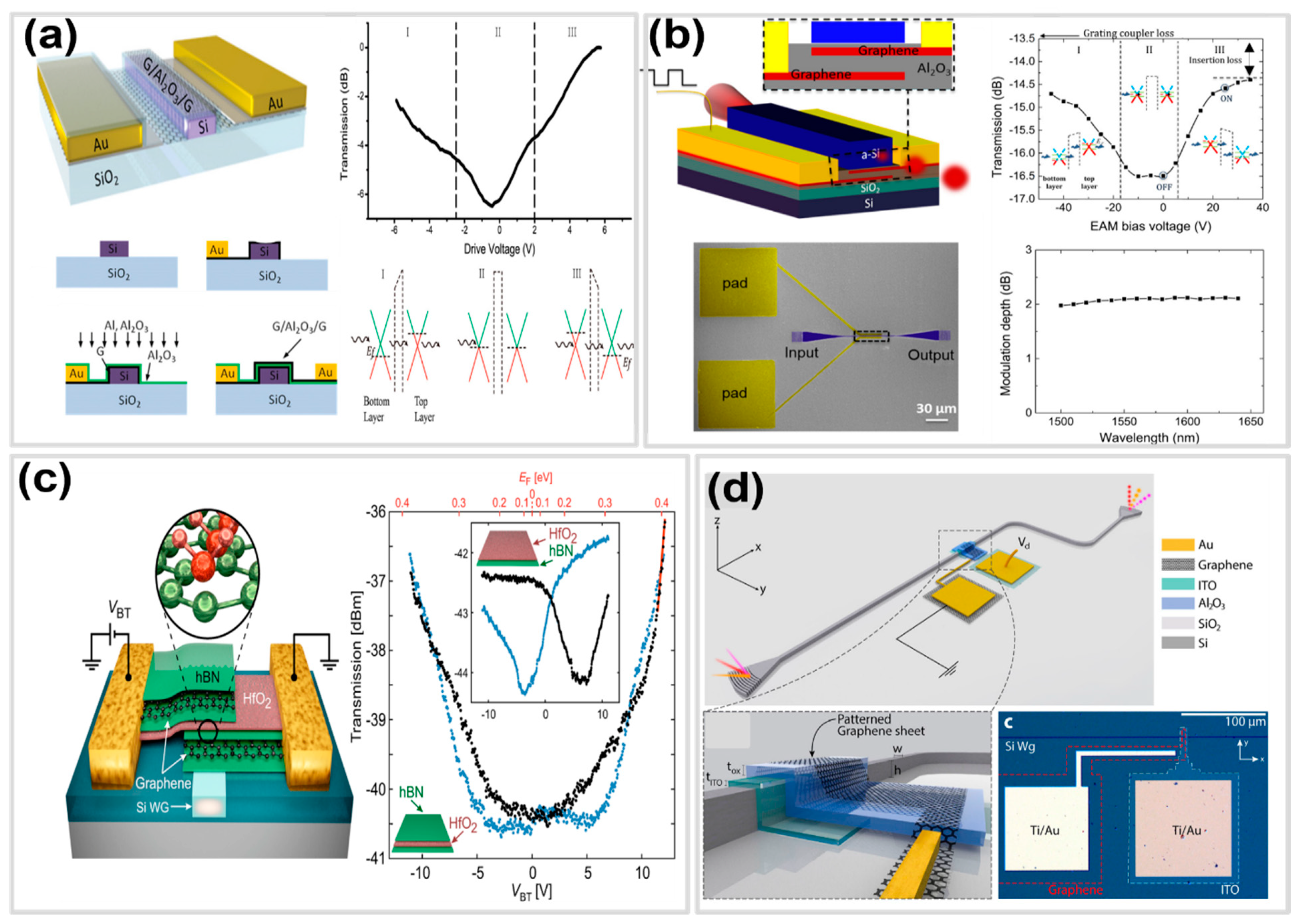
Figure 1. Graphene-assisted electro-optic modulators (a) Double-layer graphene modulator with static response and modulation depth of ~6.5 dB [35]. (b) High-speed broadband modulator with modulation depth of ~2 dB [37]. (c) hBN–HfO2–hBN-based graphene EA modulator with transmission curves as a function of the voltage between the bottom and top graphene electrodes [18], and (d) ITO-graphene heterojunction absorption modulator [38].
Table 1. Performance summary of graphene-based electro-optical modulators.
| Year | Structure | Wavelength [μm] |
Modulation Depth [dB] | Size [μm2] | Bandwidth [GHz] |
Drive Voltage | Power Consumption [fj/bit] | Ref. |
|---|---|---|---|---|---|---|---|---|
| 2011 | Si straight WG | 1.35–1.6 | 2.3 | 25 | 1.2 | 4 | 1200 | [34] |
| 2012 | Si straight WG | 1.55/3.5 | 4.77 | 63 | 120/30 | 8/3.5 | - | [39] |
| 2013 | Si PhCC | 1.57 | 10 | 108 | 300 | 1.5 | 340 | [40] |
| 2014 | Si straight WG | 1.55 | 7.042 | 225 | 2.5 | −40 | - | [41] |
| 2014 | Si MRR | 1.55 | 3.68 | 141 | - | 6 | - | [42] |
| 2015 | Si 1D grating | 1.56 | >10 | 54 | 45 | 4.8 | - | [43] |
| 2015 | Si MRR | 1.555 | 12.5 | 127 | - | 8.8 | - | [44] |
| 2015 | Si3N4 MRR | 1.57 | 15 | 1680 | 30 | 10 | 800 | [17] |
| 2016 | Si straight WG | 1.53–1.565 | 12.79 | 500 | 2.6–5.9 | 2.5 | 350 | [45] |
| 2016 | Si PhCC | 1.55 | 3.2 | 100 | 1.2 | 2.5 | 1000 | [46] |
| 2016 | Si MZI | 1.55 | 3 | - | - | 8.9 | - | [47] |
| 2018 | Si straight WG | - | 1.5 | - | 100 | - | 15 | [48] |
| 2021 | Si straight WG | - | 12 | 27 | 39 | 10.4 | - | [18] |
2.2. Graphene-Based Thermo-Optic Modulation Devices
In photonics, thermo-optic modulation is an alternative way to modulate light data. The temperature-dependent refractive index of materials, which changes as the temperature changes, is used in this method. When you change a material’s temperature, its refractive index changes. This causes changes in the phase and length of the optical path that light travels through. In the conventional silicon-based thermo-optic modulators, this modulation technique is often used by using a metallic microheater that is strategically placed near the silicon waveguide [33][49][50] or by integrating a conducting p-i-n structure closely with, or as an integral component of, the optical waveguide [51]. An important factor to take into account is the integration of a thin silicon dioxide layer, about 1 µm in thickness, between the metallic microheater and the waveguide. The primary purpose of this layer is to restrict the heating effect to the waveguide area, hence reducing the significant light absorption that is intrinsic to the metallic microheater. Nevertheless, the existence of this insulating layer presents difficulties concerning the speed and effectiveness of thermal energy transmission from the heater to the waveguide. The presence of this bottleneck results in increased power consumption and limits the achievable modulation speed. In the context of p-i-n based structures, the incorporation of carriers during modulation leads to supplementary optical losses via photonic absorption, specifically caused by mid-band donor states. The solution to these difficulties is crucial for improving the overall effectiveness and productivity of thermo-optic phase modulators in integrated photonic systems. This feature is very useful for photonic systems that need to control and modulate light. While studying silicon (Si) photonics, thermo-optic modulation has gotten a lot of attention and has been used a lot. Silicon has been used for a long time and is known for having a high thermo-optic coefficient, which means it reacts very quickly to changes in temperature. Different heat optical devices in Si photonic systems are based on this feature. As of late, adding two-dimensional (2D) materials to thermo-optic modulators, like graphene, has made new options possible. Because of its unique qualities, graphene has become a great choice for thermal devices. Its unique ability to absorb light efficiently across a wide range of spectrums makes it stand out. Graphene also has a high thermal conductivity, which means it can quickly shed heat. This makes it perfect for use in thermal uses.
Thermo-optic modulators based on graphene typically employ a waveguide structure, where graphene is integrated as a heating element. The operation relies on the thermo-optic effect, where changes in temperature induce variations in the refractive index of the waveguide material, leading to phase and intensity modulation of the guided optical signal [33][49][50]. Graphene’s excellent thermal properties ensure efficient heat generation and rapid thermal response [52], allowing for high-speed modulation with silicon devices. In 2014, Yu et al. demonstrated the first application of graphene micro-heating in silicon photonics and proposed the MZI structure-based thermo-optic modulator as shown in Figure 2a [53]. The calculated heating efficiency of the device was 11.6 K·μm3/mW as they increased the thermal conductivity of graphene by 5000 W/mK. It was further enhanced from 11.6 K·μm3/mW to 35.5 K·μm3/mW, and decaying time was reduced to 9 µs by reducing the gap between the metal pad and Si waveguide. Later, Gan et al. proposed a graphene-assisted MRR-based thermo-optic modulator [54]. They used the electrical and thermal properties of the graphene to enhance the performance of the device and achieved a high modulation depth of 7 dB with a tuning efficiency of 0.1 nm/mW. This structure was adapted by other researchers to increase the performance of the MRRs and micro-disk resonator (MDR)-based thermo-optic modulators [55][56][57][58]. In these graphene-assisted thermo-optic silicon modulators, a precise patterning technique is employed to selectively cover only the optical mode region with graphene, as opposed to the complete coverage of the entire device. By restricting the graphene coverage to the optical mode area, the modulator’s performance can be fine-tuned, enhancing its functionality in a targeted manner and effectively leveraging the inherent properties of graphene for tailored modulation capabilities [55][56]. Yu et al. experimentally demonstrated that transparent graphene nanoheaters are also a good option for other thermally tunable photonic integrated devices, as shown in Figure 2c [56]. Other than the MRR and MDR structures, Yan et al. 2017 experimentally demonstrated an energy-efficient graphene microheater on a photonic crystal waveguide with a tuning efficiency of 1.07 nm/mW [57]. The fastest rise and fall times they demonstrated were 750 ns and 525 ns, respectively. Xu et al. proposed a graphene micro-heater-based tunable silicon nanobeam cavity with a very small optical mode volume of 0.145 μm3 [58]. Because of this small optical mode volume, graphene interacted with light properly and achieved a thermo-optic tuning efficiency of 3.75 nm/mW. In this case, the rise and fall times were 1.11 µs and 1.47 µs, respectively, as shown in Figure 2b.
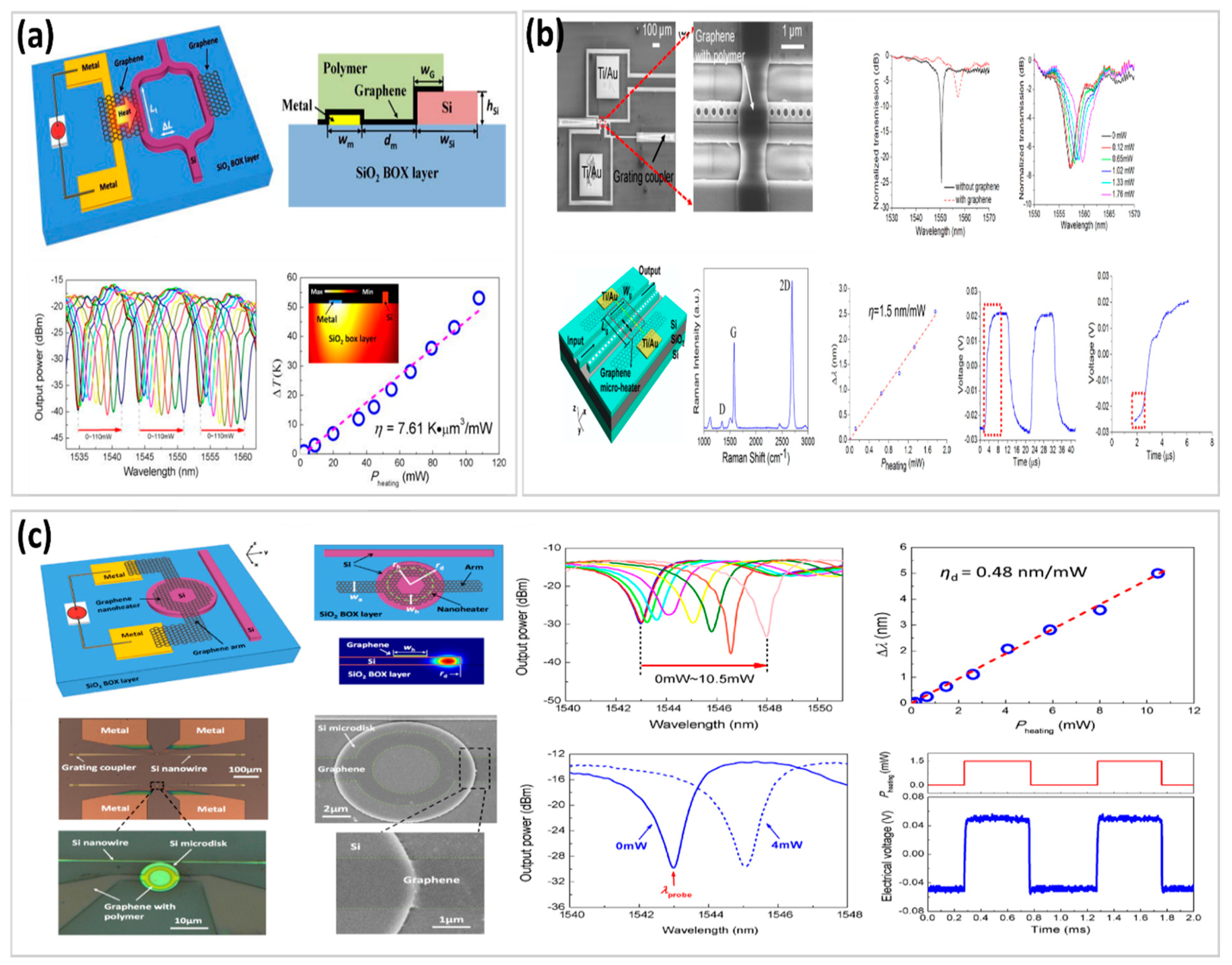
Figure 2. Graphene-assisted thermo-optic modulators. (a) Thermally tuning MZI with a non-local traditional metal heater and a graphene-based transparent flexible heat conductor [53], (b) Graphene-based silicon photonic crystal nanobeam cavity thermos-optic modulator [58], and (c) Thermally tunable silicon photonic microdisk resonator with a transparent graphene nanoheater [56].
These studies underscore the substantial merits inherent in graphene-based methodologies relative to conventional microheater techniques within the realm of silicon photonics, particularly in terms of their superior tuning efficiency and remarkable modulation speed. Graphene’s exceptional electrical and thermal properties, combined with its ultrahigh carrier mobility, confer a distinct advantage in precisely and rapidly modulating optical signals, offering a compelling alternative to traditional micro-heating methods. This technological shift holds profound implications for advancing the field of silicon photonics, enabling more efficient and faster modulation processes with potential applications spanning from telecommunications to data processing. Some different graphene-based thermos-optic modulators are demonstrated in Table 2 with their response time and the tuning efficiency parameters.
Table 2. Performance summary of graphene-based thermo-optical modulators.
3. High-Performance Graphene-Enabled Photodetectors
While an excellent waveguiding material, silicon inherently cannot be used to detect light in the telecommunication window of the electromagnetic spectrum. Therefore, researchers have investigated alternate photodetection materials to overcome this problem. Mainstream silicon photonics uses germanium (Ge) or monolayer graphene as photodetection materials. Germanium is a semiconductor with a high absorption coefficient in the C-band spectrum, making it ideal for photodetection [60][61][62][63][64][65].
Monolayer graphene, with its broad-spectrum absorption and tunability, is another attractive material for silicon photonic high-performance photodetectors. Graphene-enabled silicon photodetectors employ three distinct mechanisms—(a) Photovoltaic effect (PV), (b) Photo-bolometric effect (PB), and (c) Photo-thermoelectric effect (PTE) for photodetection, each offering unique advantages and characteristics.
3.1. Photovoltaic Effect (PV)-Based Photodetection
The first mechanism is the photovoltaic effect (PV), where incoming photons with energies exceeding the bandgap of silicon are absorbed to generate electron-hole pairs [60][61]. Xia et al. experimentally demonstrated a graphene-based photodetector up to 40 GHz in 2009 [66]. Later, Urich’s team presented measurements of the intrinsic response time of metal–graphene–metal photodetectors with monolayer graphene using an optical correlation technique with ultrashort laser pulses. They obtained a response time of 2.1 ps, mainly given by the short lifetime of the photogenerated carriers with a bandwidth of ∼262 GHz. They also showed the dependence of the response time on gate voltage and illumination laser power (Figure 3a) [67]. In graphene-based photodetectors, when light is incident normally with respect to the graphene surface, the responsivity, or the ability of the device to convert light into an electrical signal, is often relatively low. This lower responsivity can be attributed to the limited interaction of photons with an atomically thin graphene layer. Additionally, graphene’s inherently low absorption coefficient, especially in the visible and near-infrared spectrum, also contributes to this limitation.
To address this challenge and enhance the performance of graphene-based photodetectors, researchers have extensively explored the use of waveguide-based photodetectors [16][68][69][70][71]. Silicon waveguides are optical structures that can confine and guide light along a specific path, increasing the interaction length between light and the graphene layer. Integrating graphene onto the waveguide structures significantly improves the light–graphene interaction, leading to better photodetection performance [16]. These waveguide-based photodetectors are designed in such a way that incoming light is guided and channeled through the graphene layer for increased absorption. This extended interaction path allows for a higher probability of photon absorption by the graphene, resulting in improved responsivity and sensitivity of the photodetector. In this regard, Wang et al. showed that with a few layers of graphene on top of a silicon slot waveguide, a very strong absorption of light in graphene with 0.935 dB/um at the wavelength of 1.55 μm and a high responsivity of 0.273 A/W of the photodetector was achieved [63]. Schall et al. have demonstrated CVD-grown graphene on silicon waveguide-based photodetectors [72]. This device showed a maximum extrinsic response of 16 mA/W (46 mA/W absorption normalized) and a bandwidth of 41 GHz in the telecommunication band at 1.55 μm. This responsivity is approximately 80% higher than the conventional germanium-based photodetectors.
3.2. Photo-Bolometric Effect (PB)-Based Photodetection
In the photo-bolometric effect (PB), absorbed photons heat the graphene–silicon structure, changing its electrical resistance. This change in resistance is directly proportional to the incident light intensity and can be detected as a photocurrent. Plasmonic-based devices have also demonstrated superior responsivities. In hybrid plasmonic waveguides, the subwavelength confinement of the plasmonic modes gives additional advantages to enhance the light–graphene interaction. Due to the compatibility with traditional microelectronics fabrication methods, graphene-integrated hybrid plasmonic-waveguides photodetectors can also be fabricated on a large scale [69][70][71]. An integrated graphene photodetector of compact dimensions, featuring a graphene coverage length of 2.7 μm, was successfully presented by Ding et al. [69]. This photodetector exhibited an impressive unaltered response characteristic even at exceedingly high frequencies up to 110 GHz. This remarkable performance is accompanied by an intrinsic responsivity reaching 25 mA/W, signifying its exceptional sensitivity to incident light. Scaling up the device dimensions to 19 μm substantially enhanced the intrinsic responsivity to 360 mA/W. As the gap between the plasmonic slots becomes less than 50 nm, the photovoltaic (PV) mechanism starts converting into a photo-bolometric effect (PB) mechanism within the photodetection process, and this phenomenon was experimentally presented by Ma et al. (2019), as shown in Figure 3b [73]. In PB, the absorbed photons heat the graphene–silicon structure, changing its electrical resistance. This change in resistance is directly proportional to the incident light intensity and can be detected as a photocurrent. Zhizhen Ma et al. (2020) proposed a very compact plasmonic slot graphene-based photodetector with a high responsivity of 0.7 A/W [74]. In this device, they realized a 30-times-higher responsivity with a 15 nm narrower plasmonic slot, as shown in Figure 3d. The detailed discussion of graphene photodetectors based on these three mechanisms provides insights into their operation, performance, and potential applications in various photonic and optoelectronic systems by using the high absorption capability of graphene in the C-band.
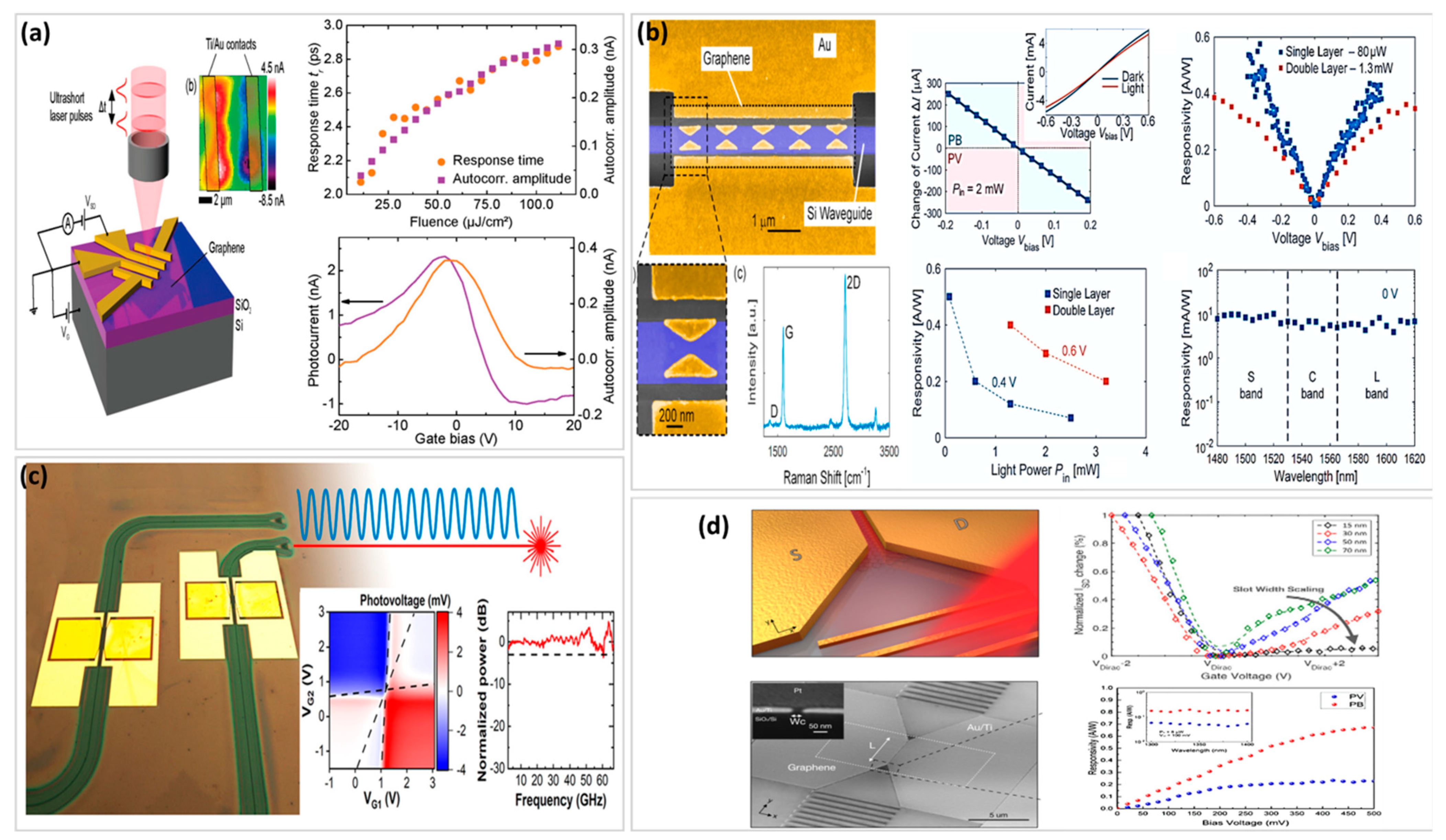
Figure 3. Graphene-assisted photodetectors. (a) Metal–graphene–metal photodetector with monolayer graphene [67]. (b) Plasmonically enhanced graphene photodetector [73]. (c) Graphene photodetector with polymeric gate dielectric on passive photonic waveguide [75], and (d) Compact graphene plasmonic slot photodetector on silicon-on-insulator [74].
3.3. Photo-Thermoelectric Effect (PTE) Based Photodetection
The photo-thermoelectric effect (PTE) in photodetectors relies on the generation of a temperature gradient within the device due to absorbed photons. This temperature gradient induces a voltage across the device, which can be measured as a photocurrent. PTE-based photodetectors are particularly efficient at detecting low-energy photons. This phenomenon is also used in the graphene-enabled silicon photodetector with the support of different structures, including MRRs) [76], photonic crystal waveguides [77], and double-layer graphene [75] to increase the performance of the device. The performance analysis of a standard silicon photodetector enhanced with graphene and cutting-edge photodetectors utilizing traditional bulk materials is presented in Table 3 for comparison. It can be seen from Table 3 that only silicon waveguide structures have limited bandwidth with limited responsivity. But, when graphene was used with the plasmonics-based photodetectors, the bandwidth was more than 110 GHz with a responsivity of 0.36 A/W. Such structures find huge promise in on-chip silicon-integrated photonic platforms. The performances of typical conventional photodetectors based on different bulk materials for comparison with state-of-art graphene based photodetectors is presented in Table 4.
Table 3. Performance summary of graphene-based photodetectors.
| Year | Structure | Wavelength [μm] |
Bandwidth [GHz] |
Responsivity (A/W) | Response Time [ps] | Ref. |
|---|---|---|---|---|---|---|
| 2013 | Si waveguide | 2.75 | - | 0.13 | - | [78] |
| 2013 | Silicon waveguide | 1.31–1.65 | 18 | 0.03 | 25 | [79] |
| 2015 | Silicon waveguide | 1.55 | 42 | 0.36 | 3 | [80] |
| 2016 | Plasmonic waveguide | 1.55 1.55 |
- - |
0.085 0.37 |
- - |
[81] |
| 2019 | Hybrid plasmonic waveguide | 1.48–1.62 | >110 | 0.5 | - | [73] |
| 2020 | Plasmonic waveguide | 1.480–1.62 | >110 | 0.36 | - | [69] |
| 2020 | Hybrid plasmonic Si waveguide | 1.55 and 2.00 | >40 | 0.4 | - | [82] |
| 2021 | Si double slot waveguide | 1.55 | 78 | 0.6 | - | [71] |
References
- Thomson, D.; Zilkie, A.; Bowers, J.E.; Komljenovic, T.; Reed, G.T.; Vivien, L.; Marris-Morini, D.; Cassan, E.; Virot, L.; Fédéli, J.M.; et al. Roadmap on silicon photonics. J. Opt. 2016, 18, 073003.
- Soref, R. The past, present, and future of silicon photonics. IEEE J. Sel. Top. Quantum Electron. 2006, 12, 1678–1687.
- Cheng, Q.; Bahadori, M.; Glick, M.; Rumley, S.; Bergman, K. Recent advances in optical technologies for data centers: A review. Optica 2018, 5, 1354.
- Michel, J.; Liu, J.; Kimerling, L.C. High-performance Ge-on-Si photodetectors. Nat. Photonics 2010, 4, 527–534.
- Bolkhovityanov, Y.B.; Pchelyakov, O.P. GaAs epitaxy on Si substrates: Modern status of research and engineering. Rev. Probl. 2008, 51, 437–456.
- Canali, C.; Majni, G.; Minder, R.; Ottaviani, G. Electron and Hole Drift Velocity Measurements in Silicon and Their Empirical Relation to Electric Field and Temperature. IEEE Trans. Electron Devices 1975, 22, 1045–1047.
- Falkovsky, L.A. Optical properties of graphene. J. Phys. Conf. Ser. 2008, 129, 012004.
- Kavitha, M.K.; Jaiswal, M. Graphene: A review of optical properties and photonic applications. Asian J. Phys. 2016, 25, 809–831. Available online: https://www.researchgate.net/publication/312070999 (accessed on 7–12 May 2023).
- Novoselov, K.S.; Geim, A.K.; Morozov, S.V.; Jiang, D.E.; Zhang, Y.; Dubonos, S.V.; Grigorieva, I.V.; Firsov, A.A. Electric Field Effect in Atomically Thin Carbon Films. Science 2016, 306, 666–669.
- Castro Neto, A.H.; Guinea, F.; Peres, N.M.R.; Novoselov, K.S.; Geim, A.K. The electronic properties of graphene. Rev. Mod. Phys. 2009, 81, 109–162.
- Balandin, A.A.; Ghosh, S.; Bao, W.; Calizo, I.; Teweldebrhan, D.; Miao, F.; Lau, C.N. Superior thermal conductivity of single-layer graphene. Nano Lett. 2008, 8, 902–907.
- Ponomarenko, L.A.; Yang, R.; Mohiuddin, T.M.; Katsnelson, M.I.; Novoselov, K.S.; Morozov, S.V.; Zhukov, A.A.; Schedin, F.; Hill, E.W.; Geim, A.K. Effect of a high-κ environment on charge carrier mobility in graphene. Phys. Rev. Lett. 2009, 102, 206603.
- Lui, C.H.; Mak, K.F.; Shan, J.; Heinz, T.F. Ultrafast photoluminescence from graphene. Phys. Rev. Lett. 2010, 105, 127404.
- Lee, B.S.; Freitas, A.P.; Gil-Molina, A.; Shim, E.; Zhu, Y.; Hone, J.; Lipson, M. Scalable graphene platform for Tbits/s data transmission. arXiv 2020, arXiv:2011.08832.
- Sun, Z.; Martinez, A.; Wang, F. Optical modulators with 2D layered materials. Nat. Photonics 2016, 10, 227–238.
- Gan, X.; Shiue, R.J.; Gao, Y.; Meric, I.; Heinz, T.F.; Shepard, K.; Hone, J.; Assefa, S.; Englund, D. Chip-integrated ultrafast graphene photodetector with high responsivity. Nat. Photonics 2013, 7, 883–887.
- Phare, C.T.; Daniel Lee, Y.H.; Cardenas, J.; Lipson, M. Graphene electro-optic modulator with 30 GHz bandwidth. Nat. Photonics 2015, 9, 511–514.
- Agarwal, H.; Terrés, B.; Orsini, L.; Montanaro, A.; Sorianello, V.; Pantouvaki, M.; Watanabe, K.; Taniguchi, T.; Van Thourhout, D.; Romagnoli, M.; et al. 2D-3D integration of hexagonal boron nitride and a high-κ dielectric for ultrafast graphene-based electro-absorption modulators. Nat. Commun. 2021, 12, 1070.
- Mueller, T.; Xia, F.; Avouris, P. Graphene photodetectors for high-speed optical communications. Nat. Photonics 2010, 4, 297–301.
- Rodrigo, D.; Limaj, O.; Janner, D.; Etezadi, D.; García De Abajo, F.J.; Pruneri, V.; Altug, H. Mid-infrared plasmonic biosensing with graphene. Science 2015, 349, 165–168.
- Chen, X.; Park, Y.J.; Kang, M.; Kang, S.K.; Koo, J.; Shinde, S.M.; Shin, J.; Jeon, S.; Park, G.; Yan, Y.; et al. CVD-grown monolayer MoS2 in bioabsorbable electronics and biosensors. Nat. Commun. 2018, 9, 1690.
- Ge, Y.; Zhu, Z.; Xu, Y.; Chen, Y.; Chen, S.; Liang, Z.; Song, Y.; Zou, Y.; Zeng, H.; Xu, S.; et al. Broadband Nonlinear Photoresponse of 2D TiS2 for Ultrashort Pulse Generation and All-Optical Thresholding Devices. Adv. Opt. Mater. 2018, 6, 1701166.
- Zhang, M.; Wu, Q.; Zhang, F.; Chen, L.; Jin, X.; Hu, Y.; Zheng, Z.; Zhang, H. 2D Black Phosphorus Saturable Absorbers for Ultrafast Photonics. Adv. Opt. Mater. 2019, 7, 1800224.
- Long, M.; Wang, P.; Fang, H.; Hu, W. Progress, Challenges, and Opportunities for 2D Material Based Photodetectors. Adv. Funct. Mater. 2019, 29, 1803807.
- Singh, Y.; Subbaraman, H. Graphene-hBN based Hybrid Plasmonic SOI Refractive Index Sensor. In CLEO 2023; Optica Publishing Group: San Jose, CA, USA, 2023; p. JTu2A.138. Available online: https://opg.optica.org/abstract.cfm?URI=CLEO_SI-2023-JTu2A.138 (accessed on 7–12 May 2023).
- Singh, Y.; Subbaraman, H. Study and analysis of the tunable plasmonic sensor based on surface conductivity of graphene. In Physics and Simulation of Optoelectronic Devices XXXI; Witzigmann, B., Osiński, M., Arakawa, Y., Eds.; SPIE: San Francisco, CA, USA, 2023; p. 124150I.
- Qing, Y.M.; Ma, H.F.; Ze Ren, Y.; Yu, S.; Tie, A.; Cui, J. Near-infrared absorption-induced switching effect via guided mode resonances in a graphene-based metamaterial. Opt. Express 2019, 27, 5253–5263.
- Qing, Y.M.; Huang, Z.; Jiang, H.; Li, B.; Li, B. Polarization-dependent thermal-tunable graphene-based metamaterial exploiting critical coupling with guided mode resonances. JOSA B 2023, 40, 233–238.
- Qing, Y.M.; Ma, H.F.; Cui, T.J.; Cui, T.J. Multifunctional space-time-coding amplitude modulated graphene metasurfaces. JOSA B 2021, 38, 3206–3211.
- Reed, G.T.; Mashanovich, G.; Gardes, F.Y.; Thomson, D.J. Silicon optical modulators. Nat. Photonics 2010, 4, 518–526.
- Xu, Q.; Schmidt, B.; Pradhan, S.; Lipson, M. Micrometre-scale silicon electro-optic modulator. Nature 2005, 435, 325–327.
- Kim, K.; Choi, J.Y.; Kim, T.; Cho, S.H.; Chung, H.J. A role for graphene in silicon-based semiconductor devices. Nature 2011, 479, 338–344.
- Fegadolli, W.S.; Vargas, G.; Wang, X.; Valini, F.; Barea, L.A.M.; Oliveira, J.E.B.; Frateschi, N.; Scherer, A.; Almeida, V.R.; Panepucci, R.R. Reconfigurable silicon thermo-optical ring resonator switch based on Vernier effect control. Opt. Express 2012, 20, 14722.
- Liu, M.; Yin, X.; Ulin-Avila, E.; Geng, B.; Zentgraf, T.; Ju, L.; Wang, F.; Zhang, X. A graphene-based broadband optical modulator. Nature 2011, 474, 64–67.
- Liu, M.; Yin, X.; Zhang, X. Double-layer graphene optical modulator. Nano Lett. 2012, 12, 1482–1485.
- Lee, B.S.; Kim, B.; Freitas, A.P.; Mohanty, A.; Zhu, Y.; Bhatt, G.R.; Hone, J.; Lipson, M. High-performance integrated graphene electro-optic modulator at cryogenic temperature. Nanophotonics 2020, 10, 99–104.
- Dalir, H.; Xia, Y.; Wang, Y.; Zhang, X. Athermal Broadband Graphene Optical Modulator with 35 GHz Speed. ACS Photonics 2016, 3, 1564–1568.
- Amin, R.; George, J.K.; Wang, H.; Maiti, R.; Ma, Z.; Dalir, H.; Khurgin, J.B.; Sorger, V.J. An ITO-graphene heterojunction integrated absorption modulator on Si-photonics for neuromorphic nonlinear activation. APL Photonics 2021, 6, 120801.
- Koester, S.J.; Li, M. High-speed waveguide-coupled graphene-on-graphene optical modulators. Appl. Phys. Lett. 2012, 100, 171107.
- Gan, X.; Shiue, R.J.; Gao, Y.; Mak, K.F.; Yao, X.; Li, L.; Szep, A.; Walker, D.; Hone, J.; Heinz, T.F.; et al. High-contrast electrooptic modulation of a photonic crystal nanocavity by electrical gating of graphene. Nano Lett. 2013, 13, 691–696.
- Youngblood, N.; Anugrah, Y.; Ma, R.; Koester, S.J.; Li, M. Multifunctional graphene optical modulator and photodetector integrated on silicon waveguides. Nano Lett. 2014, 14, 2741–2746.
- Qiu, C.; Gao, W.; Vajtai, R.; Ajayan, P.M.; Kono, J.; Xu, Q. Efficient modulation of 1.55 μm radiation with gated graphene on a silicon microring resonator. Nano Lett. 2014, 14, 6811–6815.
- Qiu, C.; Pan, T.; Gao, W.; Liu, R.; Su, Y.; Soref, R. Proposed high-speed micron-scale spatial light valve based on a silicon-graphene hybrid structure. Opt. Lett. 2015, 40, 4480.
- Ding, Y.; Zhu, X.; Xiao, S.; Hu, H.; Frandsen, L.H.; Mortensen, N.A.; Yvind, K. Effective Electro-Optical Modulation with High Extinction Ratio by a Graphene-Silicon Microring Resonator. Nano Lett. 2015, 15, 4393–4400.
- Hu, Y.; Pantouvaki, M.; Van Campenhout, J.; Brems, S.; Asselberghs, I.; Huyghebaert, C.; Absil, P.; Van Thourhout, D. Broadband 10 Gb/s operation of graphene electro-absorption modulator on silicon. Laser Photon. Rev. 2016, 10, 307–316.
- Gao, Y.; Shiue, R.J.; Gan, X.; Li, L.; Peng, C.; Meric, I.; Wang, L.; Szep, A.; Walker, D.; Hone, J.; et al. High-speed electro-optic modulator integrated with graphene-boron nitride heterostructure and photonic crystal nanocavity. Nano Lett. 2015, 15, 2001–2005.
- Phatak, A.; Cheng, Z.; Qin, C.; Goda, K. Design of electro-optic modulators based on graphene-on-silicon slot waveguides. Opt. Lett. 2016, 41, 2501–2504.
- Kovacevic, G.; Phare, C.; Set, S.Y.; Lipson, M.; Yamashita, S. Ultra-high-speed graphene optical modulator design based on tight field confinement in a slot waveguide. Appl. Phys. Express 2018, 11, 065102.
- Atabaki, A.H.; Hosseini, E.S.; Eftekhar, A.A.; Yegnanarayanan, S.; Adibi, A. Optimization of metallic microheaters for high-speed reconfigurable silicon photonics. Opt. Express 2010, 18, 18312–18323.
- Dong, P.; Qian, W.; Liang, H.; Shafiiha, R.; Feng, D.; Li, G.; Cunningham, J.E.; Krishnamoorthy, A.V.; Asghari, M. Thermally tunable silicon racetrack resonators with ultralow tuning power. Opt. Express 2010, 18, 20298.
- Harris, N.C.; Ma, Y.; Mower, J.; Baehr-Jones, T.; Englund, D.; Hochberg, M.; Galland, C. Efficient, compact and low loss thermo-optic phase shifter in silicon. Opt. Express 2014, 22, 10487.
- Khan, U.; Kim, T.H.; Lee, K.H.; Lee, J.H.; Yoon, H.J.; Bhatia, R.; Sameera, I.; Seung, W.; Ryu, H.; Falconi, C.; et al. Self-powered transparent flexible graphene microheaters. Nano Energy 2015, 17, 356–365.
- Yu, L.; Dai, D.; He, S. Graphene-based transparent flexible heat conductor for thermally tuning nanophotonic integrated devices. Appl. Phys. Lett. 2014, 105, 251104.
- Gan, S.; Cheng, C.; Zhan, Y.; Huang, B.; Gan, X.; Li, S.; Lin, S.; Li, X.; Zhao, J.; Chen, H.; et al. A highly efficient thermo-optic microring modulator assisted by graphene. Nanoscale 2015, 7, 20249–20255.
- Schall, D.; Mohsin, M.; Sagade, A.A.; Otto, M.; Chmielak, B.; Suckow, S.; Giesecke, A.L.; Neumaier, D.; Kurz, H. Infrared transparent graphene heater for silicon photonic integrated circuits. Opt. Express 2016, 24, 7871.
- Yu, L.; Yin, Y.; Shi, Y.; Dai, D.; He, S. Thermally tunable silicon photonic microdisk resonator with transparent graphene nanoheaters. Optica 2016, 3, 159.
- Yan, S.; Zhu, X.; Frandsen, L.H.; Xiao, S.; Mortensen, N.A.; Dong, J.; Ding, Y. Slow-light-enhanced energy efficiency for graphene microheaters on silicon photonic crystal waveguides. Nat. Commun. 2017, 8, 14411.
- Xu, Z.; Qiu, C.; Yang, Y.; Zhu, Q.; Jiang, X.; Zhang, Y.; Gao, W.; Su, Y. Ultra-compact tunable silicon nanobeam cavity with an energy-efficient graphene micro-heater. Opt. Express 2017, 25, 19479.
- Nakamura, S.; Sekiya, K.; Matano, S.; Shimura, Y.; Nakade, Y.; Nakagawa, K.; Monnai, Y.; Maki, H. High-Speed and On-Chip Optical Switch Based on a Graphene Microheater. ACS Nano 2022, 16, 2690–2698.
- Benedikovic, D.; Virot, L.; Aubin, G.; Amar, F.; Szelag, B.; Karakus, B.; Hartmann, J.-M.; Alonso-Ramos, C.; Le Roux, X.; Crozat, P.; et al. 25 Gbps low-voltage hetero-structured silicon-germanium waveguide pin photodetectors for monolithic on-chip nanophotonic architectures. Photonics Res. 2019, 7, 437.
- Benedikovic, D.; Virot, L.; Aubin, G.; Hartmann, J.-M.; Amar, F.; Le Roux, X.; Alonso-Ramos, C.; Cassan, E.; Marris-Morini, D.; Crozat, P.; et al. 40 Gbps heterostructure germanium avalanche photo receiver on a silicon chip. Optica 2020, 7, 775.
- Lischke, S.; Peczek, A.; Morgan, J.S.; Sun, K.; Steckler, D.; Yamamoto, Y.; Korndörfer, F.; Mai, C.; Marschmeyer, S.; Fraschke, M.; et al. Ultra-fast germanium photodiode with 3-dB bandwidth of 265 GHz. Nat. Photonics 2021, 15, 925–931.
- Wang, J.; Cheng, Z.; Chen, Z.; Wan, X.; Zhu, B.; Tsang, H.K.; Shu, C.; Xu, J. High-responsivity graphene-on-silicon slot waveguide photodetectors. Nanoscale 2016, 8, 13206–13211.
- Douhan, R.; Lozovoy, K.; Kokhanenko, A.; Deeb, H.; Dirko, V.; Khomyakova, K. Recent Advances in Si-Compatible Nanostructured Photodetectors. Technologies 2023, 11, 17.
- Seo, J.; Kim, Y.J.; Yoo, H.; Xie, J.; Mao, Z.; Seo, J.; Kim, Y.J.; Yoo, H. Zero Bias Operation: Photodetection Behaviors Obtained by Emerging Materials and Device Structures. Micromachines 2022, 13, 2089.
- Xia, F.; Mueller, T.; Lin, Y.M.; Valdes-Garcia, A.; Avouris, P. Ultrafast graphene photodetector. Nat. Nanotechnol. 2009, 4, 839–843.
- Urich, A.; Unterrainer, K.; Mueller, T. Intrinsic response time of graphene photodetectors. Nano Lett. 2011, 11, 2804–2808.
- Shu, H.; Su, Z.; Huang, L.; Wu, Z.; Wang, X.; Zhang, Z.; Zhou, Z. Significantly High Modulation Efficiency of Compact Graphene Modulator Based on Silicon Waveguide. Sci. Rep. 2018, 8, 991.
- Ding, Y.; Cheng, Z.; Zhu, X.; Yvind, K.; Dong, J.; Galili, M.; Hu, H.; Mortensen, N.A.; Xiao, S.; Oxenløwe, L.K. Ultra-compact integrated graphene plasmonic photodetector with bandwidth above 110 GHz. Nanophotonics 2020, 9, 317–325.
- Wang, Y.; Li, X.; Jiang, Z.; Tong, L.; Deng, W.; Gao, X.; Huang, X.; Zhou, H.; Yu, Y.; Ye, L.; et al. Ultrahigh-speed graphene-based optical coherent receiver. Nat. Commun. 2021, 12, 5076.
- Yan, S.Q.; Zuo, Y.; Xiao, S.S.; Oxenløwe, L.K.; Ding, Y.H. Graphene photodetector employing double slot structure with enhanced responsivity and large bandwidth. Opto-Electron. Adv. 2022, 5, 210159.
- Schall, D.; Neumaier, D.; Mohsin, M.; Chmielak, B.; Bolten, J.; Porschatis, C.; Prinzen, A.; Matheisen, C.; Kuebart, W.; Junginger, B.; et al. 50 GBit/s Photodetectors Based on Wafer-Scale Graphene for Integrated Silicon Photonic Communication Systems. ACS Photonics 2014, 1, 781–784.
- Ma, P.; Salamin, Y.; Baeuerle, B.; Josten, A.; Heni, W.; Emboras, A.; Leuthold, J. Plasmonically Enhanced Graphene Photodetector Featuring 100 Gbit/s Data Reception, High Responsivity, and Compact Size. ACS Photonics 2019, 6, 154–161.
- Ma, Z.; Kikunaga, K.; Wang, H.; Sun, S.; Amin, R.; Maiti, R.; Tahersima, M.H.; Dalir, H.; Miscuglio, M.; Sorger, V.J. Compact Graphene Plasmonic Slot Photodetector on Silicon-on-Insulator with High Responsivity. ACS Photonics 2020, 7, 932–940.
- Mišeikis, V.; Marconi, S.; Giambra, M.A.; Montanaro, A.; Martini, L.; Fabbri, F.; Pezzini, S.; Piccinini, G.; Forti, S.; Terrés, B.; et al. Ultrafast, Zero-Bias, Graphene Photodetectors with Polymeric Gate Dielectric on Passive Photonic Waveguides. ACS Nano 2020, 14, 11190–11204.
- Schuler, S.; Muench, J.E.; Ruocco, A.; Balci, O.; van Thourhout, D.; Sorianello, V.; Romagnoli, M.; Watanabe, K.; Taniguchi, T.; Goykhman, I.; et al. High-responsivity graphene photodetectors integrated on silicon microring resonators. Nat. Commun. 2021, 12, 3733.
- Schuler, S.; Schall, D.; Neumaier, D.; Schwarz, B.; Watanabe, K.; Taniguchi, T.; Mueller, T. Graphene Photodetector Integrated on a Photonic Crystal Defect Waveguide. ACS Photonics 2018, 5, 4758–4763.
- Wang, X.; Cheng, Z.; Xu, K.; Tsang, H.K.; Xu, J. Bin High-responsivity graphene/silicon-heterostructure waveguide photodetectors. Nat. Photonics 2013, 7, 888–891.
- Pospischil, A.; Humer, M.; Furchi, M.M.; Bachmann, D.; Guider, R.; Fromherz, T.; Mueller, T. CMOS-compatible graphene photodetector covering all optical communication bands. Nat. Photonics 2013, 7, 892–896.
- Shiue, R.J.; Gao, Y.; Wang, Y.; Peng, C.; Robertson, A.D.; Efetov, D.K.; Assefa, S.; Koppens, F.H.L.; Hone, J.; Englund, D. High-Responsivity Graphene-Boron Nitride Photodetector and Autocorrelator in a Silicon Photonic Integrated Circuit. Nano Lett. 2015, 15, 7288–7293.
- Goykhman, I.; Sassi, U.; Desiatov, B.; Mazurski, N.; Milana, S.; De Fazio, D.; Eiden, A.; Khurgin, J.; Shappir, J.; Levy, U.; et al. On-Chip Integrated, Silicon-Graphene Plasmonic Schottky Photodetector with High Responsivity and Avalanche Photogain. Nano Lett. 2016, 16, 3005–3013.
- Guo, J.; Li, J.; Liu, C.; Yin, Y.; Wang, W.; Ni, Z.; Fu, Z.; Yu, H.; Xu, Y.; Shi, Y.; et al. High-performance silicon−graphene hybrid plasmonic waveguide photodetectors beyond 1.55 μm. Light Sci. Appl. 2020, 9, 29.
- Salamin, Y.; Ma, P.; Baeuerle, B.; Emboras, A.; Fedoryshyn, Y.; Heni, W.; Cheng, B.; Josten, A.; Leuthold, J. 100 GHz Plasmonic Photodetector. ACS Photonics 2018, 5, 3291–3297.
- Runge, P.; Zhou, G.; Ganzer, F.; Mutschall, S.; Seeger, A. Waveguide integrated InP-based photodetector for 100Gbaud applications operating at wavelengths of 1310 nm and 1550 nm. Eur. Conf. Opt. Commun. ECOC 2015, 2015, 1–3.
- Xue, Y.; Han, Y.; Tong, Y.; Yan, Z.; Wang, Y.; Zhang, Z.; Tsang, H.K.; Lau, K.M. High-performance III-V photodetectors on a monolithic InP/SOI platform. Optica 2021, 8, 1204–1209.
- Mauthe, S.; Baumgartner, Y.; Sousa, M.; Ding, Q.; Rossell, M.D.; Schenk, A.; Czornomaz, L.; Moselund, K.E. High-speed III-V nanowire photodetector monolithically integrated on Si. Nat. Commun. 2020, 11, 4565.
More
Information
Subjects:
Engineering, Electrical & Electronic
Contributors
MDPI registered users' name will be linked to their SciProfiles pages. To register with us, please refer to https://encyclopedia.pub/register
:
View Times:
1.1K
Revisions:
2 times
(View History)
Update Date:
04 Dec 2023
Table of Contents


Notice
You are not a member of the advisory board for this topic. If you want to update advisory board member profile, please contact office@encyclopedia.pub.
OK
Confirm
Only members of the Encyclopedia advisory board for this topic are allowed to note entries. Would you like to become an advisory board member of the Encyclopedia?
Yes
No
${ textCharacter }/${ maxCharacter }
Submit
Cancel
Back
Comments
${ item }
|
${ item.createdUser.fullName }
${ item.createdAt }
${ item.vote }
${ item.reply }
Delete
${ reply.createdUser.fullName }
${ reply.createdAt }
${ reply.vote }
Delete
There is no reply to this comment~
${ item.replyTextCharacter }/${ item.replyMaxCharacter }
Submit
Cancel
More
No more~
There is no comment~
${ textCharacter }/${ maxCharacter }
Submit
Cancel
${ selectedItem.replyTextCharacter }/${ selectedItem.replyMaxCharacter }
Submit
Cancel
Confirm
Are you sure to Delete?
Yes
No