Your browser does not fully support modern features. Please upgrade for a smoother experience.
Submitted Successfully!
 +1 credit
Thank you for your contribution! You can also upload a video entry or images related to this topic.
For video creation, please contact our Academic Video Service.
| Version | Summary | Created by | Modification | Content Size | Created at | Operation |
|---|---|---|---|---|---|---|
| 1 | Shalini Prasad | -- | 3023 | 2023-11-29 16:25:10 | | | |
| 2 | Sirius Huang | Meta information modification | 3023 | 2023-11-30 02:38:22 | | |
Video Upload Options
We provide professional Academic Video Service to translate complex research into visually appealing presentations. Would you like to try it?
Cite
If you have any further questions, please contact Encyclopedia Editorial Office.
Madhurantakam, S.; Mathew, G.; David, B.E.; Naqvi, A.; Prasad, S. Transition Metal Dichalcogenides for Electrochemical Biomolecular Detection. Encyclopedia. Available online: https://encyclopedia.pub/entry/52200 (accessed on 28 July 2026).
Madhurantakam S, Mathew G, David BE, Naqvi A, Prasad S. Transition Metal Dichalcogenides for Electrochemical Biomolecular Detection. Encyclopedia. Available at: https://encyclopedia.pub/entry/52200. Accessed July 28, 2026.
Madhurantakam, Sasya, Georgeena Mathew, Bianca Elizabeth David, Aliya Naqvi, Shalini Prasad. "Transition Metal Dichalcogenides for Electrochemical Biomolecular Detection" Encyclopedia, https://encyclopedia.pub/entry/52200 (accessed July 28, 2026).
Madhurantakam, S., Mathew, G., David, B.E., Naqvi, A., & Prasad, S. (2023, November 29). Transition Metal Dichalcogenides for Electrochemical Biomolecular Detection. In Encyclopedia. https://encyclopedia.pub/entry/52200
Madhurantakam, Sasya, et al. "Transition Metal Dichalcogenides for Electrochemical Biomolecular Detection." Encyclopedia. Web. 29 November, 2023.
Copy Citation
Advances in the field of nanobiotechnology are largely due to discoveries in the field of materials. Recent developments in the field of electrochemical biosensors based on transition metal nanomaterials as transducer elements have been beneficial as they possess various functionalities that increase surface area and provide well-defined active sites to accommodate elements for rapid detection of biomolecules. In recent years, transition metal dichalcogenides (TMDs) have become the focus of interest in various applications due to their considerable physical, chemical, electronic, and optical properties.
transition metal dichalcogenides
point-of-care devices
electrochemical sensor
two-dimensional materials
biomarkers
1. Introduction
Within the evolving realm of medical device development, interest has grown exponentially in transition metal dichalcogenides (TMDs), a class of two-dimensional materials with a wide range of electrochemical properties that are used in research areas such as nanotechnology and nanosensing. Since the discovery of graphene in 2004, which represented a major milestone in materials research due to its excellent electrical properties and value for electronic applications, researchers have eagerly sought advances in TMDs [1]. Transition metal dichalcogenides have many ideal properties, such as high response rates, a high surface-to-volume ratio, low operating voltage, and compatibility with standard manufacturing processes [2]. Due to these specific characteristics, TMDs have taken the place of traditional semiconductors in the advancing era of electrochemical devices for biosensing research. The recent surge in COVID-19 and the resulting need for rapid yet accurate detection methods have caused the demand for biosensors with real-time biomolecule detection capabilities to skyrocket [3]. TMDs are emerging as a promising factor in the development of point-of-care biosensors for real-time detection of biomolecules in various pathological disease states.
Transition metal dichalcogenides consist of the MX2 form, where M is the transition metal (Mn, Mo, Cr, Ti, V, Zr, Nb, Tc, Ta, Hf, W, or Re) and X is the chalcogen (O, S, Se, Te, Po) [4]. Conventionally, transition metals are preferred due to their appealing mechanical properties, but the lack of an electronic band gap led researchers to discover 2D materials that have semiconducting properties [5]. TMD materials are layered, with the plane of metal atoms sandwiched between two opposing planes of chalcogen atoms covalently bonded in the described layer and through van der Waal (VdW) interactions between successive layers [4]. These weak van der Waal interactions allow for layer-controlled synthesis, giving TMDs unique optoelectronic properties through this reduction from multilayers to monolayers. The VdW interactions can be mechanically disrupted by exfoliation techniques such as liquid-phase exfoliation, electrochemistry, and intercalation chemistry [6]. Liquid-phase exfoliation is a promising method that yields a large amount of 2D nanosheets in a wide thickness range from tens to hundreds of nanometers and attracts much attention due to its unique physical and chemical properties [7]. The X-M-X single-layer isolation of the material causes a shift in the electronic band structure from indirect to direct, which increases the likelihood of its use in transistor fabrication due to its strong photoluminescence and large exciton binding energy [8]. The finite band gap in semiconductor materials such as TMDs is important for the research and development of electrochemical biosensors. When 2D transition metal dichalcogenides are atomically diluted into a single layer, the electrical structure shifts from an indirect to a direct band gap, which is of interest for electrochemical medical device research. TMDs with high photothermal energy show promising results in applications in biomedicine, nanoelectronics, optoelectronics, photonics, and more.
TMDs have an ultra-thin structure (approximately 0.6–0.7 nm) with a high surface-to-volume ratio, which is an ideal structure for surface adsorption of loaded biomolecules as it provides an excellent platform for anchoring the adsorbents to the sensing site [9]. This large surface-to-volume ratio of TMDs increases sensitivity and selectivity while reducing biosensor power consumption. The increased density of surface sites allows for a higher probability of binding of the analyte to the site of the transducer elements of the sensors, which allows for manipulation of the optoelectronics and thus increases the sensitivity of the biosensors [10]. TMD-based sensors bypass the step of reactivity with the targeted biomolecule. The thickness of the TMD material determines the specific properties it contains. This layered structure also allows for the transport of charge carriers and the change in volume adjustment when ions are introduced, giving it a unique chemical composition and crystal structure. The flexibility of TMDs is an added advantage of TMDs, as it allows the manipulation of the material for the synthesis of devices at the point of use. This particular focus on the atomic thickness of transition metal dichalcogenides is sparking interest in research for next-generation electronic devices for medical applications [10].
Biosensors of interest can be divided into electrical, optical, and electrochemical biosensors. Electrical biosensors have a relatively simple and easy-to-use detection method that allows real-time detection of analytes. The binding of analytes to the TMD surface results in a current change signal that converts information about the analyte [3]. Optical biosensors are sensitive because they use surface plasmon resonance (SPR), which measures the local refractive index in response to the adsorption of the analyte of interest. Optical biosensors can also use fluorescence resonance energy transfer (FRET), which involves the transfer of non-radiant energy between two coupled fluorophores [11]. This text focuses on the electrochemical-based biosensing of target analytes by measuring interfacial impedance values once the analyte of interest is applied to the surface [12]. The electrodes in the biosensors include the working electrode (WE), the reference electrode (RE), and the counter electrode (CE). The electrical potentials are measured concerning the RE, while the CE makes the connections in the electrochemical cell. The WE can be suitably modified by nanomaterials to enhance the electrochemical activity, and biological detection elements can be used to detect analytes on the surface of the electrode. Analytes adsorbed on the surface of WE result in a unique electrochemical current or interfacial impedance response after modification [13][14]. The basic operating principle involves the determination of Faraday current by voltammetry or amperometry and the manipulation of interfacial impedance by electrochemical impedance spectroscopy [1].
Two-dimensional materials have promising potential for next-generation applications in energy storage, electronics development, sensor fabrication, and biomedical applications, as shown in Figure 1. Bioanalyte detection is critical for disease diagnosis, prognosis, and treatment and can be combined with the growing interest in 2D materials in the biomedical field [10][14]. The high surface-to-volume ratio and density of surface sites make 2D materials such as transition metal dichalcogenides favorable transducer elements in various biomolecular detection methods. Finite bandgaps and layer-dependent optoelectrical properties make TMDs superior to other known metals [9].
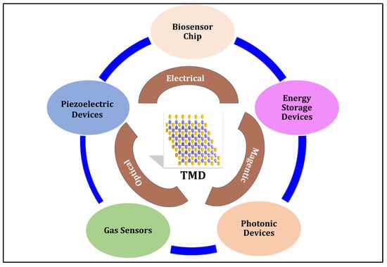
Figure 1. Overview of the structural and physical properties of transition metal dichalcogenides. Part of the figure (TMD structure) is from ref. [15].
2. Structure and Properties
In the last decade, we have witnessed the tremendous success of 2D materials, including graphene, and subsequently, transition metal dichalcogenides have received much attention due to their unique properties. Compared to graphene, TMDs exhibit a wide range of interesting properties, such as metallic (VSe2, NbS2), semimetallic (TiSe2, WTe2), semiconducting (WS2, MoS2), and insulating (HfS2) properties [16][17]. In addition, some TMDs exhibit distinguishable properties such as charge density waves, Mott transitions, and superconductivity. Interestingly, one can change the electronic properties of TMDs based on their layers (single or multilayer). Similarly, it is observed that the functional properties of TMDs can vary with the crystal structure depending on their atomic arrangement. The most common polymorphs are trigonal IT (single layers in the order AmC), hexagonal 2H (double layers in the order AmA CmC), and rhombohedral 3R (triple layers in the order AmA, BmB, CmC), where A, B, and C = chalcogenides and m = transition metal. TMDs in the 2H phase are known to be semiconducting and stable and have a large band gap in the visible region. TMDs in the 1T phase show higher reactivity compared to the 2T phase and are metallic or semimetallic in nature [17][18]. Randell nomenclature is generally used to name TMDs with a layered Van der Waals (vdW) crystal structure. In addition, the number of d-electrons can also influence the overall electronic properties of TMDs. Thus, the preferred coordination geometry and the Fermi energy (EF) depend on the orbital occupation. The elements of groups 5 and 6 prefer a trigonal–prismatic geometry, while the elements of groups 4 and 7–10 prefer an octahedral coordination. The only representative of group 8 is FeTe2, which was only recently discovered and whose research is still in progress, as shown by the small number of publications. Furthermore, the metallic or semiconducting nature of TMDs can be determined by the positioning of the Fermi energy. For example, the former has partially filled orbitals, and the EF lies within the band, while the EF lies in the energy gap in TMDs with partially filled orbitals [19][20].
3. Synthesis
TMD materials are used in various fields such as optoelectronic devices, gas sensors, environmental remediation, biosensors, energy storage, conversion, etc., due to their unique optical, electrical, and mechanical properties [1]. It is observed that intriguing and special properties can be uncovered by synthesizing thin-film TMDs in contrast to their bulk compounds. Moreover, both theoretical and experimental studies on semiconducting TMDs have revealed extraordinary properties, leading to new potential applications in the field of nanomaterials and nanodevices. Therefore, considerable efforts have been made in recent years to synthesize and develop high-quality TMDs. MoS2 and WS2 are the only TMDs that occur naturally in layered crystal form. Various methods have been used to obtain thin TMD layers, including mechanical/chemical exfoliation, chemical vapor deposition (CVD), intercalation, wet chemical methods, sonication, chemical vapor transport (CVT), and molecular beam epitaxy (MBE) [21]. These strategies can be roughly divided into top–down and bottom–up methods, as shown in Figure 2.
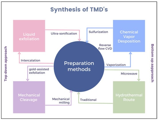
3.1. Top–Down Synthesis Methods
In the top–down synthesis route, TMDs are usually prepared by exfoliation, intercalation, and sonication. The low surface energy of many 2D TMDs (MoS2, WS2, and NbSe2) allows for easy exfoliation. The applied mechanical force splits/separates the individual layers of the source material into thin layers. The most widely used, efficient, and basic method is the scotch tape method, which overcomes the vdW attraction by applying adhesive forces [25]. However, it is extremely difficult to ensure structural integrity, control of flake size and thickness, and transfer of TMDs after synthesis if this method is to be optimized for industrial applications. Apart from the limited commercial availability of bulk TMDCs, defect-free exfoliation requires considerable effort and suffers from low reproducibility. Nevertheless, mechanical exfoliation is still considered the most popular method for synthesizing single-layer TMDs with high crystal quality and excellent electronic and optical properties. Bellus et al. used the mechanical exfoliation route to synthesize a MoSe2/WS2 heterostructure with a trion binding energy of ~62 meV [26]. Another technique is to introduce alkali metal ions for intercalation between layers and further exfoliation. However, alkali metals tend to aggregate, which is time-consuming, and this method detects impurities from the outside. Furthermore, chemical exfoliation can lead to the formation of additional intermediates with undesirable physical and chemical properties. A recent study on Li interaction as an attractive route for large-scale synthesis of single-layer MoS2 films was presented by Eda and co-workers. In the study, it was reported that exfoliation by Li intercalation resulted in a loss of the original semiconducting properties of MoS2 due to structural changes [27]. Similarly, controlled electrochemical intercalation of Li in bulk TMDs was used to synthesize a few layers of thick nanosheets of NbSe2, WSe2, Sb2Se3, and Bi2Te3 [28]. Mao et al. developed ultrathin 2D nanosheets of WSe2, MoSev, WS2, and MoS2 with a thickness of ∼3 nm and a lateral size of a few hundred nanometers by an ultrasound-assisted synthesis route. They concluded that mild liquid-phase exfoliation of bulk TMDs is a gentle exfoliation method for obtaining high-quality TMD crystals compared to other conventional methods [7].
3.2. Bottom–Up Synthesis Methods
In the bottom–up method, molecules are used as starting reagents in suitable deposition techniques and can be further divided into multicomponent or single-source precursor systems. This method mainly includes wet chemical synthesis, CVD, and MBE. The wet chemical synthesis method allows the controlled growth of TMD nanosheets. Generally, metal salts are used as starting materials for nanosheet synthesis. Wet chemical synthesis can be roughly divided into hydrothermal and solvothermal methods. In the hydrothermal method, the reaction takes place in a sealed autoclave at elevated temperature and pressure under an inert gas atmosphere. The solvothermal method is very similar to the hydrothermal method, with the only difference being that an organic solvent is used instead of water. This method also requires a sealed vessel with a reaction temperature that is above the boiling point of the solvent used. When the temperature rises above the boiling point of the solvent, the formation of TMD crystals occurs under high pressure. As a representative example, Lee et al. have shown the synthesis of MoS2 TMDs with a 1T edge using dimethylformamide (DMF) as a solvent [29].
CVD is another bottom–up technique used in the synthesis of TMDs. In this process, 2D TMDs are grown on a substrate by a reaction between the thermal evaporation of a metal precursor and thermally evaporated chalcogen elements such as selenium or sulfur. The CVD process is a powerful method for developing single or double-layer 2D materials with large dimensions. The technique offers high-quality TMD layers with controllable layer numbers, domain sizes, and excellent properties, as well as a simple and practical solution for industrial requirements. Despite these advantages, the quality of the obtained single-layer TMDs has serious drawbacks that hinder their application in nanotechnology. Moreover, CVD requires stringent conditions, such as elevated temperatures during synthesis, which leads to numerous crystallographic defects and impurities. Researchers reported the synthesis of centimeter-sized continuous films from single-layer MoS2 films directly on Si substrates with an oxide layer, also achieving large domain sizes of more than 20 μm within the films. This is achieved by orienting the growth substrate vertically to improve the uniformity of the starting material compared to horizontally oriented growth substrates [11]. Similarly, molecular beam epitaxy (MBE) is one of the first scalable methods for the synthesis of TMDs. The MBE method requires an ultra-high vacuum (UHV) with elements of high purity. The elements are heated in an effusion cell of electron beam evaporators until they slowly begin to sublime. The thermally evaporated gaseous elements react with each other and condense on the substrate. This technique enables the growth of ultra-thin crystalline heterostructures with high yields. Moreover, the crystallinity of the obtained TMD is monitored in situ by reflecting high-energy electron diffraction and low-energy electron diffraction. Epitaxial layers of WS2 using MBE are discussed, for example, by Jaeger Mann and his co-workers [30].
In addition to these techniques, there are a variety of other methods, such as the polymer-assisted transfer method, pulsed layer deposition, cation exchange, etc., that are used to develop TMDs. Finally, the TMDs synthesized by the direct route may not work well in biosensor applications. Therefore, surface modification of TMDs is a suitable method to improve their performance. Various materials, such as carbon-based materials, polymers, proteins, metal nanoparticles, MOFs, MXenes, etc., can be associated with TMDs. The main objective of performing this surface modification is to achieve improved electrochemical properties, biocompatibility, and low toxicity.
4. Electrochemical Biosensor and Application of TMDs for Detection of Biomolecules
TMDs have become increasingly popular due to their high volume-to-surface-area ratio, making them an attractive choice in various fields, including clinical applications. One particular area of interest is their use in biosensors, particularly electrochemical biosensors. In this type of biosensor, TMDs are utilized to capture target molecules that are essential to vital processes and substances that can affect life. As mentioned in Figure 3, immunosensors are used to detect target molecules such as carcinoembryonic antigens (CEA), DNA, pesticides, and forms of microcystins, while enzymatic sensors are used to detect molecules in the body such as miRNA, CRP, glucose, and H2O2. Electrochemical sensors offer additional possibilities for measuring biological molecules such as luteolin and guanine, as well as biological molecules in various pathological conditions such as Friedreich’s ataxia (FA). The other aspect related to electrochemical detection has also been reported for the detection of environmental pollutants using TMDs, especially TNT, BPA, and heavy metal ions [31]. Although TMDs have such great potential, this text focuses specifically on the methods of electrochemical detection of biological components. Transition metal dichalcogenides (TMDs), a class of graphene-like 2D materials, have attracted considerable attention in the field of electrochemical sensing. Among the various TMDs, MoS2 stands out as the most intensively studied and widely recognized material for its sensing capabilities [32]. Although other TMDs exist, MoS2 has become the main focus of research due to its remarkable performance in electrochemical sensing applications.
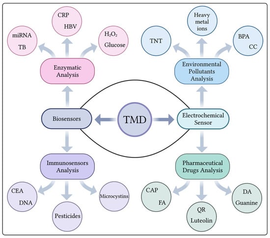
Figure 3. Applications of TMD materials for the detection of different analytes using various biosensing strategies. (Created using Biorender.com (accessed on 3 November 2023)).
TMDs have proven to be excellent candidates for electrochemical sensors, offering advantages in both simplicity and versatility. These TMDs provide a reliable platform for the detection of various molecules, including both simple and complex analytes, as depicted in Figure 4. Their large surface area enables not only efficient but also accurate detection of target molecules, resulting in higher sensitivity and selectivity. Furthermore, the unique electronic properties of MoS2 contribute to its superior electrocatalytic activity, which enables highly sensitive detection [33]. In addition to TMD’s ability to detect simple molecules, it demonstrated its potential as a biocompatible matrix for the immobilization of biomolecules. These specific properties of TMD materials enabled the development of biosensors that can detect complex molecules but also have properties that allow them to capture even small biomolecules. By integrating specific enzymes or antibodies, these biosensors can selectively recognize biomolecules and detect the target biomolecules with sensitivity and precision. The combination of TMD’s biocompatibility with the catalytic properties of enzymes creates a powerful platform for the detection of complex analytes [34]. Although there are many TMDs within the family of graphene-like 2D materials, MoS2 remains the most researched and extensively studied material due to its superior sensing capabilities. The unique properties of MoS2, combined with its frequent availability and ease of synthesis, have helped it become a popular research focus in electrochemical sensing.
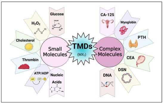
Figure 4. Utilization of TMD materials for electrochemical biosensing of small and complex molecules. (Created using Biorender.com (accessed on 3 November 2023)).
References
- Mia, A.K.; Meyyappan, M.; Giri, P.K. Two-Dimensional Transition Metal Dichalcogenide Based Biosensors: From Fundamentals to Healthcare Applications. Biosensors 2023, 13, 169.
- Hu, Y.; Huang, Y.; Tan, C.; Zhang, X.; Lu, Q.; Sindoro, M.; Huang, X.; Huang, W.; Wang, L.; Zhang, H. Two-Dimensional Transition Metal Dichalcogenide Nanomaterials for Biosensing Applications. Mater. Chem. Front. 2017, 1, 24–36.
- Tajik, S.; Dourandish, Z.; Garkani Nejad, F.; Beitollahi, H.; Jahani, P.M.; Di Bartolomeo, A. Transition Metal Dichalcogenides: Synthesis and Use in the Development of Electrochemical Sensors and Biosensors. Biosens. Bioelectron. 2022, 216, 114674.
- Walsh, L.A.; Addou, R.; Wallace, R.M.; Hinkle, C.L. Molecular Beam Epitaxy of Transition Metal Dichalcogenides. In Molecular Beam Epitaxy; Elsevier: Amsterdam, The Netherlands, 2018; pp. 515–531.
- Manzeli, S.; Ovchinnikov, D.; Pasquier, D.; Yazyev, O.V.; Kis, A. 2D Transition Metal Dichalcogenides. Nat. Rev. Mater. 2017, 2, 17033.
- Rojas, D.; Della Pelle, F.; Del Carlo, M.; Compagnone, D.; Escarpa, A. Group VI Transition Metal Dichalcogenides as Antifouling Transducers for Electrochemical Oxidation of Catechol-Containing Structures. Electrochem. Commun. 2020, 115.
- Zhang, J.; Ji, T.; Jin, H.; Wang, Z.; Zhao, M.; He, D.; Luo, G.; Mao, B. Mild Liquid-Phase Exfoliation of Transition Metal Dichalcogenide Nanosheets for Hydrogen Evolution. ACS Appl. Nano Mater. 2022, 5, 8020–8028.
- Akanksha Urade. Properties of TMDs The State of Art: Synthesis of TMDs. Available online: https://www.azonano.com/article.aspx?ArticleID=5988 (accessed on 3 November 2023).
- Wang, Y.H.; Huang, K.J.; Wu, X. Recent Advances in Transition-Metal Dichalcogenides Based Electrochemical Biosensors: A Review. Biosens. Bioelectron. 2017, 97, 305–316.
- Choi, W.; Choudhary, N.; Han, G.H.; Park, J.; Akinwande, D.; Lee, Y.H. Recent Development of Two-Dimensional Transition Metal Dichalcogenides and Their Applications. Mater. Today 2017, 20, 116–130.
- Damborský, P.; Švitel, J.; Katrlík, J. Optical biosensors. Essays Biochem. 2016, 60, 91–100.
- Wang, X.; Deng, W.; Shen, L.; Yan, M.; Yu, J. A 3D Electrochemical Immunodevice Based on an Au Paper Electrode and Using Au Nanoflowers for Amplification. New J. Chem. 2016, 40, 2835–2842.
- Madhurantakam, S.; Babu, K.J.; Rayappan, J.B.B.; Krishnan, U.M. Nanotechnology-Based Electrochemical Detection Strategies for Hypertension Markers. Biosens. Bioelectron. 2018, 116, 67–80.
- Sasya, M.; Shalini Devi, K.S.; Babu, J.K.; Rayappan, J.B.B.; Krishnan, U.M. Metabolic Syndrome—An Emerging Constellation of Risk Factors: Electrochemical Detection Strategies. Sensors 2019, 20, 103.
- Duraisamy, S.; Ganguly, A.; Sharma, P.K.; Benson, J.; Davis, J.; Papakonstantinou, P. One-Step Hydrothermal Synthesis of Phase-Engineered MoS2/MoO3Electrocatalysts for Hydrogen Evolution Reaction. ACS Appl. Nano Mater. 2021, 4, 2642–2656.
- Brune, V.; Grosch, M.; Weißing, R.; Hartl, F.; Frank, M.; Mishra, S.; Mathur, S. Influence of the Choice of Precursors on the Synthesis of Two-Dimensional Transition Metal Dichalcogenides. Dalton Trans. 2021, 50, 12365–12385.
- Splendiani, A.; Sun, L.; Zhang, Y.; Li, T.; Kim, J.; Chim, C.Y.; Galli, G.; Wang, F. Emerging Photoluminescence in Monolayer MoS2. Nano Lett. 2010, 10, 1271–1275.
- Chen, E.; Xu, W.; Chen, J.; Warner, J.H. 2D Layered Noble Metal Dichalcogenides (Pt, Pd, Se, S) for Electronics and Energy Applications. Mater. Today Adv. 2020, 7, 100076.
- Satheesh, P.P.; Jang, H.S.; Pandit, B.; Chandramohan, S.; Heo, K. 2D Rhenium Dichalcogenides: From Fundamental Properties to Recent Advances in Photodetector Technology. Adv. Funct. Mater. 2023, 33, 2212167.
- Sotthewes, K.; Van Bremen, R.; Dollekamp, E.; Boulogne, T.; Nowakowski, K.; Kas, D.; Zandvliet, H.J.W.; Bampoulis, P. Universal Fermi-Level Pinning in Transition-Metal Dichalcogenides. J. Phys. Chem. C 2019, 123, 5411–5420.
- Han, S.A.; Bhatia, R.; Kim, S.W. Synthesis, Properties and Potential Applications of Two-Dimensional Transition Metal Dichalcogenides. Nano Converg. 2015, 2, 17.
- Zhao, M.; Hao, Y.; Zhang, C.; Zhai, R.; Liu, B.; Liu, W.; Wang, C.; Jafri, S.H.M.; Razaq, A.; Papadakis, R.; et al. Advances in Two-Dimensional Materials for Optoelectronics Applications. Crystals 2022, 12, 1087.
- Kandhasamy, D.M.; Muthu Mareeswaran, P.; Chellappan, S.; Namasivayam, D.; Aldahish, A.; Chidambaram, K. Synthesis and Photoluminescence Properties of MoS2/Graphene Heterostructure by Liquid-Phase Exfoliation. ACS Omega 2022, 7, 629–637.
- Li, J.; Ma, Y.; Li, Y.; Li, S.S.; An, B.; Li, J.; Cheng, J.; Gong, W.; Zhang, Y. Interface Influence on the Photoelectric Performance of Transition Metal Dichalcogenide Lateral Heterojunctions. ACS Omega 2022, 7, 39187–39196.
- Budania, P.; Baine, P.T.; Montgomery, J.H.; McNeill, D.W.; Mitchell, S.J.N.; Modreanu, M.; Hurley, P.K. Comparison between Scotch Tape and Gel-Assisted Mechanical Exfoliation Techniques for Preparation of 2D Transition Metal Dichalcogenide Flakes. Micro. Nano Lett. 2017, 12, 970–973.
- Bellus, M.Z.; Ceballos, F.; Chiu, H.Y.; Zhao, H. Tightly Bound Trions in Transition Metal Dichalcogenide Heterostructures. ACS Nano 2015, 9, 6459–6464.
- Eda, G.; Yamaguchi, H.; Voiry, D.; Fujita, T.; Chen, M.; Chhowalla, M. Photoluminescence from Chemically Exfoliated MoS2. Nano Lett. 2011, 11, 5111–5116.
- Zeng, Z.; Sun, T.; Zhu, J.; Huang, X.; Yin, Z.; Lu, G.; Fan, Z.; Yan, Q.; Hng, H.H.; Zhang, H. An Effective Method for the Fabrication of Few-Layer-Thick Inorganic Nanosheets. Angew. Chem.-Int. Ed. 2012, 51, 9052–9056.
- Lee, J.E.; Jung, J.; Ko, T.Y.; Kim, S.; Kim, S.I.; Nah, J.; Ryu, S.; Nam, K.T.; Lee, M.H. Catalytic Synergy Effect of MoS2/Reduced Graphene Oxide Hybrids for a Highly Efficient Hydrogen Evolution Reaction. RSC Adv. 2017, 7, 5480–5487.
- Tiefenbacher, S.; Sehnert, H.; Pettenkofer, C.; Jaegermann, W. Surface Science Letters Epitaxial Films of WS, by Metal Organic van Der Waals Epitaxy (MO-VDWEI. Surf. Sci. 1994, 318, L1161–L1164.
- Vilian, A.T.E.; Dinesh, B.; Kang, S.M.; Krishnan, U.M.; Huh, Y.S.; Han, Y.K. Recent Advances in Molybdenum Disulfide-Based Electrode Materials for Electroanalytical Applications. Microchim. Acta 2019, 186, 203.
- Lv, R.; Robinson, J.A.; Schaak, R.E.; Sun, D.; Sun, Y.; Mallouk, T.E.; Terrones, M. Transition Metal Dichalcogenides and beyond: Synthesis, Properties, and Applications of Single- and Few-Layer Nanosheets. Acc Chem Res 2015, 48, 56–64.
- Bollella, P.; Fusco, G.; Tortolini, C.; Sanzò, G.; Favero, G.; Gorton, L.; Antiochia, R. Beyond Graphene: Electrochemical Sensors and Biosensors for Biomarkers Detection. Biosens. Bioelectron. 2017, 89, 152–166.
- Zhang, Z.; Li, W.; Yuen, M.F.; Ng, T.W.; Tang, Y.; Lee, C.S.; Chen, X.; Zhang, W. Hierarchical Composite Structure of Few-Layers MoS2 Nanosheets Supported by Vertical Graphene on Carbon Cloth for High-Performance Hydrogen Evolution Reaction. Nano Energy 2015, 18, 196–204.
More
Information
Subjects:
Electrochemistry
Contributors
MDPI registered users' name will be linked to their SciProfiles pages. To register with us, please refer to https://encyclopedia.pub/register
:
View Times:
725
Revisions:
2 times
(View History)
Update Date:
30 Nov 2023
Table of Contents


Notice
You are not a member of the advisory board for this topic. If you want to update advisory board member profile, please contact office@encyclopedia.pub.
OK
Confirm
Only members of the Encyclopedia advisory board for this topic are allowed to note entries. Would you like to become an advisory board member of the Encyclopedia?
Yes
No
${ textCharacter }/${ maxCharacter }
Submit
Cancel
Back
Comments
${ item }
|
${ item.createdUser.fullName }
${ item.createdAt }
${ item.vote }
${ item.reply }
Delete
${ reply.createdUser.fullName }
${ reply.createdAt }
${ reply.vote }
Delete
There is no reply to this comment~
${ item.replyTextCharacter }/${ item.replyMaxCharacter }
Submit
Cancel
More
No more~
There is no comment~
${ textCharacter }/${ maxCharacter }
Submit
Cancel
${ selectedItem.replyTextCharacter }/${ selectedItem.replyMaxCharacter }
Submit
Cancel
Confirm
Are you sure to Delete?
Yes
No