 +1 credit
| Version | Summary | Created by | Modification | Content Size | Created at | Operation |
|---|---|---|---|---|---|---|
| 1 | Dencho Spassov | -- | 3201 | 2023-09-05 11:52:58 | | | |
| 2 | Camila Xu | -1 word(s) | 3200 | 2023-10-20 10:05:56 | | |
Video Upload Options
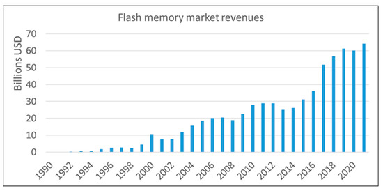
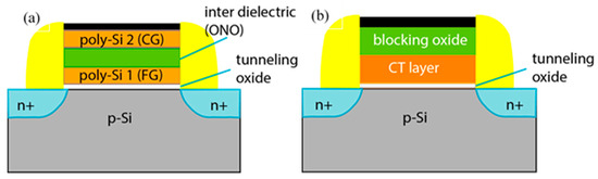
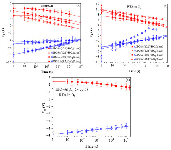
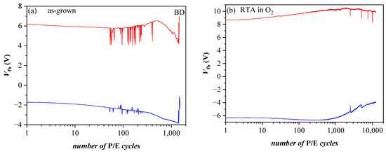
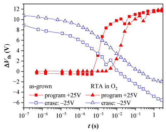
Flash memory is an electronic, non-volatile information storage device that can be electrically erased and reprogrammed. Ideally, the information stored in such a device should be preserved for long when the power is switched off. There are two flash memories designs at present: floating gate and charge trapping. Both of them work by storage of electrical charges in the space above the channel of the MOSFET. The charge storage volume of the flash cell, either poly-Si floating gate or charge trapping dielectric/dielectric stack is confined between blocking and tunnel oxides for electrical insulation from the gate electrode and Si substrate. Blocking and tunnelling oxides are important parts of the flash memory cells, as they affect retention, endurance and program/erase speed performance.
1. Introduction
2. Tunneling and Blocking Oxides
References
- Yinug, F. The Rise of the Flash Memory Market: Its Impact on Firm Behavior and Global Semiconductor Trade Patterns. J. Int. Commer. Econ. 2007. Available online: https://www.usitc.gov/publications/332/journals/rise_flash_memory_market_0.pdf (accessed on 10 March 2023).
- Patel, D. The History and Timeline of Flash Memory. Available online: https://www.semianalysis.com/p/the-history-and-timeline-of-flash (accessed on 7 August 2023).
- The Statistic Portal. 2013–2021. Available online: https://www.statista.com (accessed on 10 March 2023).
- Yoshimitsu, Y.; Yoshinari, K.; Toshimasa, M. Scalable Virtual-Ground Multilevel-Cell Floating-Gate Flash Memory. IEEE Trans. Electron. Devices 2013, 60, 2518–2524.
- Goda, A. Recent Progress on 3D NAND Flash Technologies. Electronics 2021, 10, 3156.
- Kahng, D.; Sze, S.M. A Floating Gate and Its Application to Memory Devices. Bell Syst. Tech. J. 1967, 46, 1288.
- Chen, A. A review of emerging non-volatile memory (NVM) technologies and applications. Solid-State Electron. 2016, 125, 25–38.
- International Roadmap for Devices and Systems (IRDS™) 2021 Edition. Available online: https://irds.ieee.org/editions/2021 (accessed on 13 March 2023).
- Rosmeulen, M.; Van Houdt, J. NAND Flash: The Industry’s Workhorse for Data Storage Applications. IMEC. Available online: https://www.imec-int.com/en/articles/role-3d-nand-flash-and-fefet-data-storage-roadmap (accessed on 13 March 2023).
- Dimitrakis, P. Charge-Trapping Non-Volatile Memories; Dimitrakis, P., Ed.; Springer: Cham, Switzerland, 2015.
- Zhao, C.; Zhao, C.Z.; Taylor, S.; Chalker, P.R. Review on Non-Volatile Memory with High-k Dielectrics: Flash for Generation Beyond 32 nm. Materials 2014, 7, 5117–5145.
- Park, G.H.; Cho, W.J. Reliability of modified tunneling barriers for high performance nonvolatile charge trap flash memory application. Appl. Phys. Lett. 2010, 96, 043503.
- Wegner, H.A.R.; Lincoln, A.J.; Pao, H.C.; O’Connel, M.R.; Oleksiak, R.E.; Lawrence, H. The variable threshold transistor, a new electrically-alterable, non-destructive read-only storage device. IEDM Tech. Dig. 1967, 13, 70.
- Hwang, C.S. Prospective of Semiconductor Memory Devices: From Memory System to Materials. Adv. Electron. Mater. 2015, 1, 1400056.
- Ramkumar, K. Charge trapping NVMs with metal oxides in the memory stack. In Metal Oxides for Non-Volatile Memory: Materials, Technology and Application; Dimitrakis, P., Valov, I., Tappertzhofen, S., Eds.; Elsevier: Amsterdam, The Netherlands, 2022; pp. 79–107.
- Lee, C.H.; Hur, S.H.; Shin, Y.C.; Choi, J.H.; Park, D.G.; Kim, K. Charge-trapping device structure of SiO2/SiN/high-k dielectric Al2O3 for high-density flash memory. Appl. Phys. Lett. 2005, 86, 152908.
- Seo, Y.J.; Kim, K.C.; Kim, H.D.; Joo, M.S.; An, H.M.; Kim, T.G. Correlation between charge trap distribution and memory characteristics in metal/oxide/nitride/oxide/silicon devices with two different blocking oxides, Al2O3 and SiO2. Appl. Phys. Lett. 2008, 93, 063508.
- Hou, Z.; Wu, Z.; Yin, H. Performance enhancement for charge trapping memory by using Al2O3/HfO2/Al2O3 tri-layer high-κ dielectrics and high work function metal gate. ECS J. Solid State Sci. Technol. 2018, 7, N91–N95.
- Agrawal, K.; Yoon, G.; Kim, J.; Chavan, G.; Kim, J.; Park, J.; Phong, P.; Cho, E.; Yi, J. Improving Retention Properties of ALD-AlxOy Charge trapping layer for non-volatile memory application. ECS J. Solid State Sci. Technol. 2020, 9, 043002.
- Spassov, D.; Paskaleva, A.; Guziewicz, E.; Wozniak, W.; Stanchev, T.; Ivanov, T.; Wojewoda-Budka, J.; Janusz-Skuza, M. Charge storage and reliability characteristics of nonvolatile memory capacitors with HfO2/Al2O3-based charge trapping layers. Materials 2022, 15, 6285.
- Arreghini, A.; Zahid, M.B.; Van den Bosch, G.; Suhane, A.; Breuil, L.; Cacciato, A.; Van Houdt, J. Effect of high temperature annealing on tunnel oxide properties in TANOS devices. Microelectron. Eng. 2011, 88, 1155–1158.
- Lin, C.-H.; Hsu, B.-C.; Lee, M.H.; Liu, C.W. A Comprehensive Study of Inversion Current in MOS Tunneling Diodes. IEEE Trans. Electron. Dev. 2001, 48, 2125–2130.
- Ramkumar, K.; Prabhakar, V.; Kapre, R. Scalable SONOS Based Embedded Non-Volatile Memory Technology. Available online: https://sst.semiconductor-digest.com/ (accessed on 7 August 2023).
- Seo, Y.J.; An, H.M.; Kim, H.D.; Kim, T.G. Improved Performance in Charge-Trap-Type Flash Memories with an Al2O3 Dielectric by Using Bandgap Engineering of Charge-Trapping Layers. J. Korean Phys. Soc. 2009, 55, 2689–2692.
- Chen, T.-S.; Wu, K.-H.; Chung, H.; Kao, C.-H. Performance Improvement of SONOS Memory by Bandgap Engineering of Charge-Trapping Layer. IEEE Electr. Dev. Lett. 2004, 25, 205–206.
- Jeong, J.-K.; Sung, J.-Y.; Ko, W.-S.; Nam, K.-R.; Lee, H.-D.; Lee, G.-W. Physical and Electrical Analysis of Poly-Si Channel Effect on SONOS Flash Memory. Micromachines 2021, 12, 1401.
- Vianello, E.; Driussi, F.; Arreghini, A.; Palestri, P.; Esseni, D.; Selmi, L.; Akil, N.J.; van Duuren, M.; Golubović, D.S. Experimental and Simulation Analysis of Program/Retention Transients in Silicon Nitride-Based NVM Cells. IEEE Trans. Electr. Dev. 2009, 56, 1980–1990.
- Fu, J.; Singh, N.; Buddharaju, K.D.; Teo, S.H.; Shen, C.; Jiang, Y.; Zhu, C.X.; Yu, M.B.; Lo, G.Q.; Balasubramanian, N.; et al. Si-nanowire based gate-all-around nonvolatile SONOS memory cell. IEEE Electron. Dev. Lett. 2008, 29, 518–521.
- Gnani, E.; Reggiani, S.; Gnudi, A.; Baccarani, G.; Fu, J.; Singh, N.; Lo, G.Q.; Kwong, D.L. Modeling of gate-all-around charge trapping SONOS memory cells. Solid-State Electron. 2010, 54, 997–1002.

