Your browser does not fully support modern features. Please upgrade for a smoother experience.
Submitted Successfully!
 +1 credit
Thank you for your contribution! You can also upload a video entry or images related to this topic.
For video creation, please contact our Academic Video Service.
| Version | Summary | Created by | Modification | Content Size | Created at | Operation |
|---|---|---|---|---|---|---|
| 1 | Zhi-Quan Liu | -- | 3542 | 2023-08-15 12:08:30 | | | |
| 2 | Lindsay Dong | Meta information modification | 3542 | 2023-08-17 02:45:47 | | |
Video Upload Options
We provide professional Academic Video Service to translate complex research into visually appealing presentations. Would you like to try it?
Cite
If you have any further questions, please contact Encyclopedia Editorial Office.
Chen, K.; Gao, L.; Li, Z.; Sun, R.; Liu, Z. Electroplated Nanotwinned Copper in Microelectronic Packaging. Encyclopedia. Available online: https://encyclopedia.pub/entry/48081 (accessed on 13 June 2026).
Chen K, Gao L, Li Z, Sun R, Liu Z. Electroplated Nanotwinned Copper in Microelectronic Packaging. Encyclopedia. Available at: https://encyclopedia.pub/entry/48081. Accessed June 13, 2026.
Chen, Ke-Xin, Li-Yin Gao, Zhe Li, Rong Sun, Zhi-Quan Liu. "Electroplated Nanotwinned Copper in Microelectronic Packaging" Encyclopedia, https://encyclopedia.pub/entry/48081 (accessed June 13, 2026).
Chen, K., Gao, L., Li, Z., Sun, R., & Liu, Z. (2023, August 15). Electroplated Nanotwinned Copper in Microelectronic Packaging. In Encyclopedia. https://encyclopedia.pub/entry/48081
Chen, Ke-Xin, et al. "Electroplated Nanotwinned Copper in Microelectronic Packaging." Encyclopedia. Web. 15 August, 2023.
Copy Citation
Copper is the most common interconnecting material in the field of microelectronic packaging, which is widely used in advanced electronic packaging technologies. However, with the trend of the miniaturization of electronic devices, the dimensions of interconnectors have decreased from hundreds of microns to tens of or even several microns, which has brought serious reliability issues. As a result, nanotwinned copper (nt-Cu) has been proposed as a potential candidate material and is being certified progressively.
nanotwinned copper
microelectronic packaging
electrodeposition
property
reliability
1. Introduction
With the emergence of integrated circuit (IC) technologies, the development of electronic devices is altering from day to day. Moore’s law proposed in 1965 is no longer suitable for IC development at present. Advanced packaging technologies are the key pathway to achieving “More than Moore”. Packaging methods have evolved from plating through hole (PTH), the pin grid array (PGA), and the ball grid array (BGA) in the last century to the multichip module (MCM) and the multidimensional structure. Since the start of the 21st century, new information-processing systems with dramatically improved energy efficiency and performance are partly based on advanced packaging technologies, such as flip-chip and wafer-level packaging. The interconnection form has evolved from the initial wire bonding to under-bump metallization (UBM), copper pillars (CuPs), redistribution layers (RDLs), through-silicon vias (TSVs), etc.
UBM is an indispensable technology for the purpose of soldering metal pads and tin balls, as shown in Figure 1a. The functions of UBM include the following: (a) a bonding layer for interconnection; (b) preventing atomic diffusion between tin balls and a bottom material; and (c) binding a layer of dielectric material and a metal layer. As the interconnection density increased, CuP technology appeared. Increasing the volume (thickness) of rigid copper and decreasing the volume of solder can decrease the pitch of a solder joint and increase the diffusion barrier ability. RDLs can reconfigure or redistribute pads from the perimeter footprint to alternative locations on a chip, enabling wafer bumping as shown in Figure 1b [1]. Therefore, the use of RDLs allows the utilization of a greater area of the chip and enables the use of simple, less expensive substrates. TSVs realize the electrical interconnection between chips in the vertical direction, as shown in Figure 1b. As a result, TSV-based 3D IC technology can dramatically reduce the volume of electronic devices.
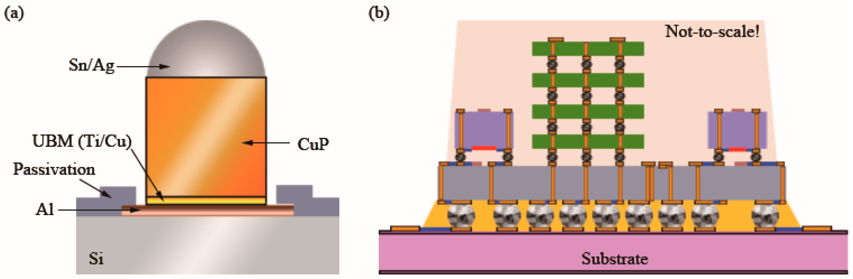
Figure 1. Schematic diagram of the cross-section of (a) a CuP and UBM on a wafer and (b) a heterogeneous integration of various chips on a TSV (orange perpendicular line) interposer with RDLs (in blue) [2].
Meanwhile, the decreasing size and pitch of RDLs, UBM, CuPs, and TSVs put a great challenge on the reliability of interconnection technologies. Although interconnection materials have changed from traditional aluminum (Al) and its alloys to current, mainstream copper (Cu) [3], after IC technology entered the 32 nm node, an interconnector’s maximum effective current-carrying density is far away from the demand. Reliability problems, including voids, electromigration (EM), and the dielectric breakdown of copper interconnections, hinder the further development of ICs [4]. In addition, the effect of EM is becoming increasingly prominent. In recent years, researchers have developed several potential interconnection technologies, such as carbon-based interconnection technology [5], optical interconnection technology [6], etc. In this case, nanotwinned copper (nt-Cu) interconnections have also been raised as a modified version of copper interconnection, and nt-Cu has been widely reported as one of the potential materials to cater to the reliability requirement of interconnections [7][8][9][10]. In 2004, K. Lu’s group found that nt-Cu exhibited ultrahigh strength and high electrical conductivity [11]. Followed closely by other researchers, some excellent physical properties of nt-Cu have also been discovered [12][13][14][15]. Since then, nt-Cu has been continuously studied as a vigorous substitute for common Cu in different fields, such as applications for aggressive radiation environments [16], a growth substrate for boron nitride [17], electrocatalytic water splitting [18], and an electrode current collector in lithium-ion batteries [19][20]. In 2012, Chih Chen’s group [21] utilized nt-Cu as a UBM for the unidirectional growth of solder bumps, signifying a landmark event of nt-Cu applied in electronic packaging interconnecting materials. Up to now, there has been a great quantity of research on nt-Cu in microelectronic packaging technologies, focusing on preparation methods, microstructure characterization, physical property optimization, and reliability evaluations, as shown in Figure 2.
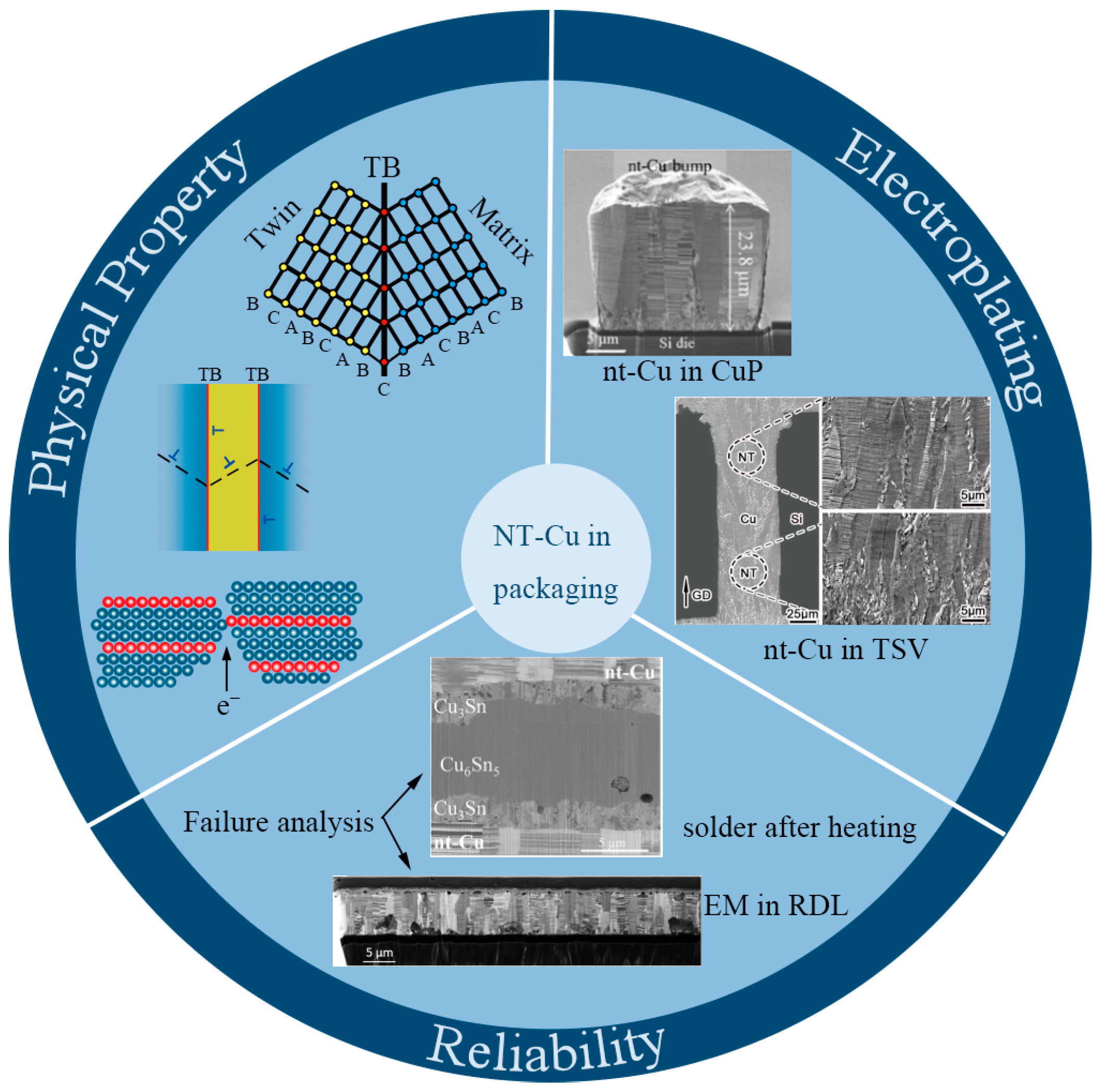
Figure 2. Property–electroplating–reliability interrelationship of nt-Cu materials [21][22][23][24][25][26]. TB represents the twin boundary. A, B and C represent atomic arrangements. “T” symbols represent dislocations. Red dots represent the atoms of TB. Other color dots represent the atoms of matrix.
Compared with traditional commercial Cu, nt-Cu has achieved an overall superior performance in advanced packaging.
2. Microstructure and Property Optimization of nt-Cu
2.1. Lattice and Atomic Arrangement of nt-Cu
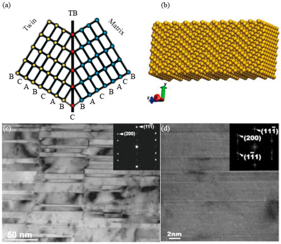
During the growth of Cu grains, atoms located on the (111) plane have two sequences, i.e., a normal sequence (-A-B-C-A-B-C-A-B-C-A-B-) and a twin fault sequence (-A-B-C-A-B-C-B-A-C-B-A-). They are also called normal nucleation and twinned nucleation, respectively [27]. The -B-C-B- sequence is equivalent to a stacking fault, and the grains (or two parts of one grain) on both sides of the C-axis (also called the coherent twin boundary, CTB) show mirror symmetry, as shown in Figure 3a. The structure of an nt-Cu supercell is shown in Figure 3b [28]. The difference between nt-Cu and cg-Cu is that there can be seen a high density of nanotwins of the {111}/[112] type growing in grains of nt-Cu, and the twin boundaries (TBs) are perfectly coherent [11]. The CTBs are clear lines, as shown in Figure 3c, and they are atomically sharp, as observed in the high-resolution transmission electron microscopy (TEM) images of Figure 3d [29][30].
Figure 3. Schematic illustrations of (a) crystal lattices of grains with a twin boundary [22] (A, B and C represent atomic arrangements. Red dots represent atoms which composed of TB. Other colored areas represent there is no TB arrangement.) and (b) the nanotwinned structure of an nt-Cu supercell [28]. (c) TEM image of Cu with twin planes oriented vertical to the growth direction. Inserted SAD pattern confirms typical twin pattern [29]. (d) HRTEM micrograph of nt-Cu showing that the planar defects are growth twins with {111} interfaces. The inserted fast Fourier transform of the image shows spot splitting across the {111} twin interfaces [30].
2.2. Mechanical Properties of nt-Cu
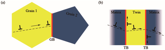
Solid alloying, cold working, and grain refinement are common strengthening methods of metals. However, they all have side effects on ductility and electric conductivity. According to the traditional Hall–Petch relationship, strength is inversely proportional to the square root of grain size due to the difficulty of dislocations transferring from one grain to the next through the barriers of incoherent internal grain boundaries, as shown in Figure 4a [22]. However, the accumulation of dislocations in grains brings a significant increase in location stress. The stress cannot be relaxed in the tensile strain-to-failure test, so the brittleness of fcc metals increases and the ductility decreases. The maximum strain before fracture decreases, and the formation of necking and cracks are accelerated after yielding [31]. Different from incoherent boundaries with high interfacial energy, coherent internal grain boundaries, such as twin boundaries with low interfacial energy, not only can effectively block dislocation movement but also can relax local stress, as shown in Figure 4b. When the twin spacing is at the micrometer level, the annealing TB displays comparable strength to a conventional grain boundary (GB), and both of them conform to the Hall–Petch (H–P) relation [32]. The atoms of CTBs are shared by grains on the sides without atomic misfits. This kind of boundary can block dislocation motion and store dislocations. Deformation in the tensile strain-to-failure test is influenced by the interaction of dislocations and CTBs. Some categories of dislocation can cross-slip on or be transmitted across CTBs, which can effectively relax the local stress after yielding. Therefore, mechanical strength and ductility are both promoted in films with CTBs.
Figure 4. Schematic illustrations of the strengthening method in (a) common grains and (b) grains with TBs [22]. Red lines represent the GBs and TBs. Other colored areas represent homo-orientation lattices. “T” symbols represent dislocations. Arrows indicate the direction of dislocation movement.
2.3. Electrical Properties of nt-Cu
GBs can capture or scatter electrons according to previous studies [11]. Therefore, the conductivity of Cu decreases if inducing GBs in a film. However, K. Lu’s group [11] found that an nt-Cu film had a similar conductivity in comparison with a cg-Cu film. Kim and coworkers [33] measured the independent resistance of different types of GBs through four-probe scanning tunneling microscopy (STM) directly. The degree of GBs scattering electrons depended on the symmetry of grains, and the resistivity of Σ3 (TB) was calculated at about 0.202 × 10⁻¹² Ω/cm2, which was from one to two orders of magnitude lower than that of other random boundaries. O. Angeroglu and coworkers [29] prepared epitaxial Cu with {111} nanotwins on single-crystal Cu substrates and found that these epitaxial nt-Cu films exhibited better conductivity than columnar-grain nt-Cu films.
2.4. Thermal Stability and Corrosion and Oxidation Resistance of nt-Cu
In the past, the thermal stability of nanostructured metals has been improved by alloying to reduce the recrystallization kinetics. In 2008, O. Anderoglu and coworkers [34] investigated the thermal stability of nt-Cu films under the condition of high-vacuum annealing up to 800 °C for 1 h. The results proved that a low-angle CTB arrangement in the films could exhibit better thermal stability than monolithic nanocrystals with high-angle GBs. In 2011, C. Saldana and coworkers [35] argued that thermal instability may link to excess vacancy concentration and that reducing vacancy supersaturation could reduce the driving force and mobility for the evolution of a microstructure and improve the thermal stability of Cu. A smaller vacancy supersaturation was represented in densely twinned samples, and this may be the reason why nt-Cu exhibited better thermal stability.
Nt-Cu also has a better performance in corrosion resistance than that of common polycrystalline Cu under high-temperature and high-humidity conditions [10]. In 2015, Chien-Neng Liao’s group [36] investigated the effect of TB spacing on the surface chemical reactivity of Cu nanowires (NWs) and found that the nt-Cu NWs exhibited a surface structure with low atomic step density when the TB spacing was less than 10 nm. The atomic step density decreased with the decrease in TB spacing in the surface, leading to high chemical reactivity and excellent corrosion resistance. The conclusion was that the structure with high nanotwin density and thinner TB spacing on the surface had superior corrosion resistance.
3. Electroplating nt-Cu in the Field of Microelectronic Packaging
Many methods can be used to produce TBs in Cu foils, such as dynamic plastic deformation [37], phase transformation [11], annealing [38], magnetron sputtering [29][30][39][40], and electroplating. Among them, electroplating is the most common and vital technology to realize electrical interconnection due to its simple operation (room temperature, normal pressure) and low cost. Therefore, the electroplating method of nt-Cu also possesses the highest compatibility with microelectronic packaging applications.
3.1. Electroplating Process of nt-Cu
3.1.1. Effect of Pulse Parameters
It was regarded that the pulse electric field should be one of the methods to generate nanotwins [41]. From a thermodynamic point of view [28][42], a pulse electric field with a high peak current density in its on time (ton) and no current density in its off time (toff), alternatively, can achieve rapid deposition and renucleation, respectively. Cu2+ ions in the vicinity of the electrode are depleted greatly during ton, and the nucleation sites increase accordingly. During toff, the Cu2+ ions can be replenished, and recrystallization substitutes for grain growth, which may facilitate twin formation.
In detail, Di Xu and coworkers [28] studied the influences of stress/strain on the formation of nanotwins through first-principle calculations and proposed that strain-relaxed nanotwins formed during the recrystallization process when biaxial stress was applied and the strain was large enough in a Cu film. Therefore, stress generation and relaxation occurred during the pulse on time and off time, respectively, forming nanotwins in the PED process. The in situ stress was measured during the PED process of Cu films and showed an increase in tensile stress to about 400 MPa during ton = 0.1 s and stress relaxation during toff = 9.9 s [42]. This result demonstrated that stress relaxation during toff was the consequence of nanotwin formation. Xiaofei Zhan and coworkers [43] observed a spiral feature of a hexagonal pyramid on the top of nt-Cu films, and the formation of periodic twin structures could be the result of the screw-dislocation-induced growth, which could also be seen in the twinned SiC nanowires [44].
3.1.2. Effects of Other Influencing Factors
The roles of influencing factors, such as current density and temperature, are discussed in both PED and DC electrodeposition, too. Current density can determine the existence and orientation of twins on a premise where the concentration of Cu2+ ions is constant for either PED or DC electrodeposition. According to the Winand diagram, a larger cathode current density, a lower concentration of Cu2+ ions, and higher inhibition intensity are conducive to the formation of twins. In addition, Cu deposits transform from the basis-oriented reproduction (BR) type to the field-oriented texture (FT) type, of which (111) nt-Cu can be a special form [45]. The growth potential in the PED process can alter the twin orientation from the horizontal to the vertical direction. In detail, Madoka Hasegawa and coworkers [46] prepared horizontal nt-Cu at −0.2 V vs. a saturated calomel electrode (SCE) and vertical nt-Cu at −0.6 V vs. an SCE with the PFD process.
3.2. Electroplating Solutions of nt-Cu
In the beginning, the simple electrolyte of CuSO4 with some acidity could obtain nt-Cu films through PED processes [11]. Later, researchers found that some organic molecules could promote nanotwin growth during the DC electroplating process. Yu Bai and coworkers [47] fabricated vertical nt-Cu with a (220) texture through DC electroplating at a high current density of about 3–5 A/dm2 (ASD) with commercial additives. In 2022, Zhong-Guo Li and coworkers [48] demonstrated that gelatin could work as an inhibitor in the DC electrodeposition process with electrochemical measurements. The inhibition intensity of gelatin was proportional to its concentration. The selective adsorption of gelatin on the (111) surface of Cu resulted in the transformation of a Cu film from the (110)-preferred vertical nt-Cu (vnt-Cu) to the (111)-preferred horizontal nt-Cu (hnt-Cu). When the content of gelatin exceeded the saturated concentration, the texture of the Cu film changed from a columnar crystal to an equiaxed crystal.
3.2.1. Effect of Acidity
The acidity of an electrolyte also affects the growth of twins. Chih Chen’s group [49] reported that the addition of H2SO4 ranging from 50 to 110 g/L in CuSO4-based electrolytes could control the growth of twins under different current densities. The Cu2+ worked as the main conductive ion when no acid was in the electrolyte, while H+ replaced this role when acid was added. In this case, the diffusion of Cu2+ was influenced by concentration gradients. Therefore, sulfuric acid could inhibit the growth of columnar nt-Cu. Zhi-Quan Liu’s group [50] also studied the effect of acidity on the microstructure of Cu films. An increased concentration of sulfuric acid promoted the formation of twins, which further led to a thinner transition layer.
3.2.2. Effect of Additives
Adding additives is the key to achieving perfect pattern filling. However, the role of additives in the electrolyte may be detrimental to the growth nt-Cu. Therefore, how to balance superb filling ability and a high density of nanotwins is the primary challenge to using nt-Cu materials in the field of microelectronic packaging.
As a general rule, accelerators are small molecules with sulfur atoms and negative electrification in the plating bath. In 2022, Yu-Xi Wang and coworkers [51] controlled the concentration of MPS to obtain dense hnt-Cu. Damascene vias with an aspect ratio of 1.4:1.4 (unit: μm:μm) could be filled without voids using co-additives containing PEG and 40 ppm of MPS.
As the most confidential ingredient in commercial electroplating solutions, leveler plays a vital role in filling. Usually, the molecules of leveler provide negative electrification in a bath containing nitrogen atoms. Levelers can be adsorbed on a protrusion area with a high current density to achieve a leveling effect. Common levelers include JGB, diazine black (DB), dodecyl trimethyl ammonium chloride (DTAC), etc. Jing Huang and coworkers [52] tried to improve filling performance by adding additives. Methylene blue was used as an additive at first during the DC electroplating process. A high-density nanotwin structure was formed from bottom to top when the concentration of methylene blue was 2 mg/L.
3.3. Electroplating nt-Cu Applied in Microelectronic Packaging
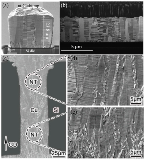
Modified electrolyte and electroplating processes of nt-Cu films have been applied in microelectronic packaging technology, such as UBM, CuPs, RDLs, and TSVs, as shown in Figure 5.
Figure 5. Cross-sectional FIB images of (a) electroplated nt-Cu bumps [24]. (b) nt-Cu RDLs along the long axis [26]. (c–e) The microstructure of an nt-Cu-filled through-silicon via (TSV) [25].
4. Reliability of nt-Cu in Electronic Packaging
4.1. Interfacial Reaction Layers
The anisotropic microstructure of nt-Cu is one of the concerning issues for the applications of interfacial reaction layers in advanced packaging. Chih Chen’s group [53] fabricated Cu pillars in the nanoscale with various orientations to investigate the stress–relaxation behavior of nt-Cu. With the use of an in situ Picoindenter under constant strain and in situ TEM, dislocations disappeared quickly due to much shorter paths in nanopillars with twin orientations parallel to the axial direction of the pillars (NT-0°), which was different from that in Cu bulk or in Cu thin film. On the contrary, a long distance increased the dislocation density on the (111) plane by dislocations piled up in nanopillars. In addition, the nanopillars with a twin orientation vertical to the axial direction of the pillar (NT-90°) had a short path to the free surface, which changed the mechanical property from bulk nt-Cu. In conclusion, a dislocation-reduced region in the NT-0° nanopillar under constant strain caused worse stress–relaxation behavior than that of the NT-90° nanopillar that maintained a high dislocation density.
4.2. Redistribution Layers (RDLs)
Yu-Jin Li and coworkers [54] confirmed potential applications of nt-Cu RDLs with a yield strength range of 300–700 MPa and an elongation rate range of 5–25%. The thermal strains of nt-Cu and regular Cu RDLs at various temperatures were analyzed by X-ray nanodiffraction [55]. In the results, the maximum stress of nt-Cu was 344.6 MPa at 434 K, which was 7.4% greater than that of the neighbor area, while the maximum stress of regular Cu was 363.8 MPa. The maximum thermal strain or stress appeared at the corner of the RDL where the line turned 90°, and the stress gradient in the corner might have caused the early failure in the thermal cyclic tests. Later, Yu-Bo Zhang and coworkers [56] also electroplated nt-Cu RDLs and achieved superior uniformity and flatness compared to three other commercial copper electrolytes.
Wafer warpage is caused by the diversity of materials used in RDLs and the complicacy of constitutive models during deformation restricting the development of RDLs. Gong Cheng and coworkers [57] suggested that introducing nanotwins in Cu RDLs relaxed great stress at the initial cooling and reduced the total thermal stress during the cooling process from 400 °C to ambient temperature, further reducing the wafer warpage introduced by Cu RDLs effectively.
4.3. Through-Silicon Vias (TSVs)
As early as 2018, Fu-Long Sun and coworkers [25] prepared columnar nt-Cu TSVs. TSVs were checked by nanoindentation from bottom to top, and the hardness was 2.34 GPa at the top and 2.63 GPa at the bottom. The small difference (0.29 GPa) between the top and the bottom sides of the nt-Cu TSVs verified the uniformity of the filled nt-Cu TSVs. Compared with the hardness for Cu TSVs without twins (1.73 GPa), the high mechanical properties of nt-Cu provided a framework to prevent wafer warpage during the later wafer-thinning process.
4.4. Other Applications in Microelectronic Packaging
In addition to UBM, CuPs, RDLs, and TSVs, there have also been some applications reported on in recent years, such as reaction layers with Ag solder pastes [58], low-temperature Cu–Cu direct bonding, and Damascene vias [51]. Among them, low-temperature Cu–Cu direct bonding is the most hotly researched and has reaped wide attention.
Zhi-Quan Liu’s group [58] used nt-Cu as the substrate of a sinter, and the bonding strength of (111)-oriented nt-Cu with Ag paste was better than that of random-oriented Cu. The bonding strength of Cu paste on an nt-Cu film could be up to 53.7 MPa at the sintering condition of 300 °C, and the value on common Cu film was 31.3 MPa.
Traditional interconnect alloys, such as lead-free Sn-based alloy solders, has become unsuitable for the relatively low resistance of electromigration and thermomigration in 3D fine-pitch packaging. From this perspective, researchers have proposed Cu–Cu direct bonding [24][59]. It has been noticed that Cu–Cu bonding can be achieved at room temperature under ultrahigh vacuum conditions and 300 °C thermal compression over 30 min under normal vacuum conditions and that the latter can save a lot of time. However, conventional solders only need a welding temperature below 250 °C, so the key to the development of Cu–Cu bonds is to successfully realize the bonding under a normal vacuum below 250 °C. Jia-Juen Ong and coworkers [60] achieved low-temperature and low-pressure (111)-oriented nt-Cu–SiO2 hybrid bonding. The bonding temperature could be lowered to 200 °C with a pressure of 1.06 MPa, which had a very low specific contact resistance of 1.2 × 10⁻⁹ Ω/cm2 and excellent thermal stability up to 375 °C. The Cu–Cu direct bonding using (111)-oriented nt-Cu could be accounted for by a surface diffusion creep-assisted bonding mechanism [24][61].
5. Conclusions
The superior physical properties of nt-Cu have caused nt-Cu materials to maintain a high level of research fervor. Secondly, the electroplating process and electrolytes of nt-Cu in recent decades were summarized. The growth mechanism of nanotwins and key influencing factors were discussed from the aspects of the electrical field, the hydrodynamics field, and the chemical field. Thirdly, nt-Cu has good performances in various applications of microelectronic packaging, such as UBM, CuPs, RDLs, TSVs, and Cu–Cu bonding.
References
- Zheng, Z.; Huang, Y.-T.; Wang, Z.; Zhang, M.; Wang, W.-T.; Chung, C.-C.; Cherng, S.-J.; Tsai, Y.-H.; Li, P.-C.; Lu, Z.; et al. Electrodeposition of (111)-oriented and nanotwin-doped nanocrystalline Cu with ultrahigh strength for 3D IC application. Nanotechnology 2021, 32, 225702.
- Lau, J.-H. Heterogeneous Integrations; Springer: Singapore, 2019.
- Baklanov, M.R.; Adelmann, C.; Zhao, L.; De Gendt, S. Advanced Interconnects: Materials, Processing, and Reliability. ECS J. Solid State Sci. Technol. 2014, 4, Y1–Y4.
- Cheng, Y.-L.; Lee, C.-Y.; Huang, Y.-L. Copper Metal for Semiconductor Interconnects. In Noble and Precious Metals; Mohindar Singh, S., Alan, D.B., Eds.; IntechOpen: Rijeka, Croatia, 2018.
- Wei, Q. Progress in research on carbon nanotubes interconnection. J. Funct. Mater. Devices 2012, 18, 63–69.
- Taubenblatt, M.-A. Optical Interconnects for High-Performance Computing. J. Lightwave Technol. 2012, 30, 448–457.
- Amanov, A. Microstructural evolution and mechanical properties of Cu-based alloy by post-sintering ultrasonic nanocrystal surface modification. Mater. Lett. 2022, 308, 131124.
- Zhao, H.-Z.; You, Z.-S.; Tao, N.-R.; Lu, L. Anisotropic toughening of nanotwin bundles in the heterogeneous nanostructured Cu. Acta Mater. 2022, 228, 117748.
- Kou, Z.; Huang, R.; Yang, Y.; Feng, T.; Tang, S.; Lan, S.; Yang, L. Revealing the atomic-scale evolution of sessile disconnections on twin boundaries during deformation. Scr. Mater. 2022, 221, 114956.
- Shi, Z.; Gao, L.-Y.; Zhang, Y.-B.; Liu, Z.-Q. The serving behavior of nanotwinned copper under the reliability test of high temperature high humidity and electromigration test. In Proceedings of the 2022 23rd International Conference on Electronic Packaging Technology (ICEPT), Dalian, China, 10–13 August 2022.
- Lu, L.; Shen, Y.; Chen, X.; Qian, L.; Lu, K. Ultrahigh Strength and High Electrical Conductivity in Copper. Science 2004, 304, 422–426.
- Lu, L.; Schwaiger, R.; Shan, Z.-W.; Dao, M.; Lu, K.; Suresh, S. Nano-sized twins induce high rate sensitivity of flow stress in pure copper. Acta Mater. 2005, 53, 2169–2179.
- Shen, Y.-F.; Lu, L.; Lu, Q.-H.; Jin, Z.-H.; Lu, K. Tensile properties of copper with nano-scale twins. Scr. Mater. 2005, 52, 989–994.
- Zhang, Y.-S.; Wang, K.; Han, Z.; Liu, G. Dry sliding wear behavior of copper with nano-scaled twins. Wear 2007, 262, 1463–1470.
- Cheng, Z.; Zhou, H.; Lu, Q.; Gao, H.; Lu, L. Extra strengthening and work hardening in gradient nanotwinned metals. Science 2018, 362, eaau1925.
- Fan, C.-C.; Xie, D.-Y.; Li, J.; Shang, Z.-X.; Chen, Y.-X.; Xue, S.-C.; Wang, J.; Li, M.-M.; El-Azab, A.; Wang, H.-Y.; et al. 9R phase enabled superior radiation stability of nanotwinned Cu alloys via in situ radiation at elevated temperature. Acta Mater. 2019, 167, 248–256.
- Li, X.; Li, Y.; Wang, Q.; Yin, J.; Li, J.; Yu, J.; Guo, W. Oxygen-suppressed selective growth of monolayer hexagonal boron nitride on copper twin crystals. Nano Res. 2017, 10, 826–833.
- Huang, C.-L.; Sasaki, K.; Senthil-Raja, D.; Hsieh, C.-T.; Wu, Y.-J.; Su, J.-T.; Cheng, C.-C.; Cheng, P.-Y.; Lin, S.-H.; Choi, Y.-M.; et al. Twinning Enhances Efficiencies of Metallic Catalysts toward Electrolytic Water Splitting. Adv. Energy Mater. 2021, 11, 2101827.
- Cheng, H.-Y.; Tran, D.-P.; Tu, K.-N.; Chen, C. Effect of deposition temperature on mechanical properties of nanotwinned Cu fabricated by rotary electroplating. Mater. Sci. Eng. A 2021, 811, 141065.
- Lin, C.-C.; Chen, Z.; Euchner, H.; Eisenmann, T.; Geng, K.; Diemant, T.; Fang, S.; Yen, C.-H.; Passerini, S.; Hu, C.-C.; et al. Nanotwinned Copper Foil for “Zero Excess” Lithium–Metal Batteries. ACS Appl. Energ. Mater. 2023, 6, 2140–2150.
- Hsiao, H.-Y.; Liu, C.-M.; Lin, H.-W.; Liu, T.-C.; Lu, C.-L.; Huang, Y.-S.; Chen, C.; Tu, K.-N. Unidirectional growth of microbumps on (111)-oriented and nanotwinned copper. Science 2012, 336, 1007–1010.
- Lu, K.; Lu, L.; Suresh, S. Strengthening Materials by Engineering Coherent Internal Boundaries at the Nanoscale. Science 2009, 324, 349–352.
- Shen, F.-C.; Huang, C.-Y.; Lo, H.-Y.; Hsu, W.-Y.; Wang, C.-H.; Chen, C.; Wu, W.-W. Atomic-Scale Investigation of Electromigration with Different Directions of Electron Flow into High-Density Nanotwinned Copper through In Situ HRTEM. Acta Mater. 2021, 219, 117250.
- Juang, J.-Y.; Lu, C.-L.; Chen, K.-J.; Chen, C.-A.; Hsu, P.-N.; Chen, C.; Tu, K.-N. Copper-to-copper direct bonding on highly (111)-oriented nanotwinned copper in no-vacuum ambient. Sci. Rep. 2018, 8, 13910.
- Sun, F.-L.; Liu, Z.-Q.; Li, C.-F.; Zhu, Q.-S.; Zhang, H.; Suganuma, K. Bottom-Up Electrodeposition of Large-Scale Nanotwinned Copper within 3D Through Silicon Via. Materials 2018, 11, 319.
- Tseng, I.-H.; Hsu, P.-N.; Lu, T.-L.; Tu, K.-N.; Chen, C. Electromigration failure mechanisms of <111>-oriented nanotwinned Cu redistribution lines with polyimide capping. Results Phys. 2021, 24, 104154.
- Chan, T.-C.; Lin, Y.-M.; Tsai, H.-W.; Wang, Z.-M.; Liao, C.-N.; Chueh, Y.-L. Growth of large-scale nanotwinned Cu nanowire arrays from anodic aluminum oxide membrane by electrochemical deposition process: Controllable nanotwin density and growth orientation with enhanced electrical endurance performance. Nanoscale 2014, 6, 7332–7338.
- Xu, D.; Kwan, W.-L.; Chen, K.; Zhang, X.; Ozoliņš, V.; Tu, K.-N. Nanotwin formation in copper thin films by stress/strain relaxation in pulse electrodeposition. Appl. Phys. Lett. 2007, 91, 254105.
- Anderoglu, O.; Misra, A.; Wang, H.; Ronning, F.; Hundley, M.-F.; Zhang, X. Epitaxial nanotwinned Cu films with high strength and high conductivity. Appl. Phys. Lett. 2008, 93, 083108.
- Zhang, X.; Wang, H.; Chen, X.-H.; Lu, L.; Lu, K.; Hoagland, R.-G.; Misra, A. High-strength sputter-deposited Cu foils with preferred orientation of nanoscale growth twins. Appl. Phys. Lett. 2006, 88, 173116.
- Park, S.-W.; Eom, H.-W.; Kim, M.-J.; Kim, J.-J. Electrodeposition of Nano-Twinned Cu and their Applications in Electronics. J. Electrochem. Soc. 2022, 169, 112503.
- Lu, L. Current Progress of Mechanical Properties of Metals with Nano-scale Twins. J. Mater. Sci. Technol. 2008, 24, 473–482.
- Kim, T.-H.; Zhang, X.-G.; Nicholson, D.-M.; Evans, B.-M.; Kulkarni, N.-S.; Radhakrishnan, B.; Kenik, E.-A.; Li, A.-P. Large discrete resistance jump at grain boundary in copper nanowire. Nano Lett. 2010, 10, 3096–3100.
- Anderoglu, O.; Misra, A.; Wang, H.; Zhang, X. Thermal stability of sputtered Cu films with nanoscale growth twins. J. Appl. Phys. 2008, 103, 094322.
- Saldana, C.; King, A.-H.; Stach, E.-A.; Compton, W.-D.; Chandrasekar, S. Vacancies, twins, and the thermal stability of ultrafine-grained copper. Appl. Phys. Lett. 2011, 99, 231911.
- Huang, C.-L.; Liao, C.-N. Chemical reactivity of twin-modified copper nanowire surfaces. Appl. Phys. Lett. 2015, 107, 021601.
- Zhao, W.; Tao, N.; Guo, J.; Lu, Q.; Lu, K. High density nano-scale twins in Cu induced by dynamic plastic deformation. Scr. Mater. 2005, 53, 745–749.
- Roy, B.; Das, J. Strengthening face centered cubic crystals by annealing induced nano-twins. Sci. Rep. 2017, 7, 17512.
- Hodge, A.-M.; Wang, Y.-M.; Barbee, T.-W. Large-scale production of nano-twinned, ultrafine-grained copper. Mater. Sci. Eng. A 2006, 429, 272–276.
- Hodge, A.-M.; Wang, Y.-M.; Barbee, T.-W. Mechanical deformation of high-purity sputter-deposited nano-twinned copper. Scr. Mater. 2008, 59, 163–166.
- Natter, H.; Schmelzer, M.; Hempelmann, R. Nanocrystalline nickel and nickel-copper alloys: Synthesis, characterization, and thermal stability. J. Mater. Res. 1998, 13, 1186–1197.
- Xu, D.; Sriram, V.; Ozolins, V.; Yang, J.-M.; Tu, K.-N.; Stafford, G.-R.; Beauchamp, C. In situ measurements of stress evolution for nanotwin formation during pulse electrodeposition of copper. J. Appl. Phys. 2009, 105, 023521.
- Zhan, X.; Lian, J.; Li, H.; Wang, X.; Zhou, J.; Trieu, K.; Zhang, X. Preparation of highly (111) textured nanotwinned copper by medium-frequency pulsed electrodeposition in an additive-free electrolyte. Electrochim. Acta 2021, 365, 137391.
- Chen, J.; Pan, Y.; Wu, R. Growth mechanism of twinned SiC nanowires synthesized by a simple thermal evaporation method. Physica E 2010, 42, 2335–2340.
- Winand, R. Electrodeposition of metals and alloys—New results and perspectives. Electrochim. Acta 1994, 39, 1091–1105.
- Hasegawa, M.; Mieszala, M.; Zhang, Y.; Erni, R.; Michler, J.; Philippe, L. Orientation-controlled nanotwinned copper prepared by electrodeposition. Electrochim. Acta 2015, 178, 458–467.
- Bai, Y.; Hu, H.; Ling, H.; Hang, T.; Hu, A.; Wu, Y.; Li, M. Communication—Fabrication of Vertical Nanotwinned Copper with (220) Texture by Direct Current Electrodeposition. J. Electrochem. Soc. 2021, 168, 082506.
- Li, Z.-G.; Gao, L.-Y.; Li, Z.; Sun, R.; Liu, Z.-Q. Regulating the orientation and distribution of nanotwins by trace of gelatin during direct current electroplating copper on titanium substrate. J. Mater. Sci. 2022, 57, 17797–17811.
- Tseng, C.-H.; Chen, C. Growth of Highly (111)-Oriented Nanotwinned Cu with the Addition of Sulfuric Acid in CuSO4 Based Electrolyte. Cryst. Growth Des. 2018, 19, 81–89.
- Sun, F.-L.; Gao, L.-Y.; Liu, Z.-Q. Electrodeposition of nanotwinned copper film as under bump metallization. In Proceedings of the 2017 18th International Conference on Electronic Packaging Technology (ICEPT), Harbin, China, 16–19 August 2017.
- Wang, Y.-X.; Gao, L.-X.; Wan, Y.-Q.; Liu, Z.-Q. Pulse Electroplating of Nanotwinned Copper using MPS-PEG Two-additive System for Damascene via Filling Process. J. Electrochem. 2022.
- Huang, J.; Li, Z.-G.; Gao, L.-Y. Effect of methylene blue on the microstructure and mechanical properties of nanotwinned copper during DC electroplating. J. Integr. Technol. 2021, 10, 55–62.
- Shen, Y.-A.; Chang, L.; Chang, S.-Y.; Chou, Y.-C.; Tu, K.-N.; Chen, C. Nanotwin orientation on history-dependent stress decay in Cu nanopillar under constant strain. Nat. Nanotechnol. 2022, 33, 155708.
- Li, Y.-J.; Tu, K.-N.; Chen, C. Tensile Properties of <111>-Oriented Nanotwinned Cu with Different Columnar Grain Structures. Materials 2020, 13, 1310.
- Hsu, W.-Y.; Tseng, I.-H.; Chiang, C.-Y.; Tu, K.-N.; Chen, C. Distribution of elastic stress as a function of temperature in a 2-μm redistribution line of Cu measured with X-ray nanodiffraction analysis. J. Mater. Res. Technol JMRT 2022, 20, 2799–2808.
- Zhang, Y.-B.; Gao, L.-Y.; Li, X.; Li, Z.; Ma, X.-L.; Liu, Z.-Q.; Sun, R. Electroplating nanotwinned copper for ultrafine pitch redistribution layer (RDL) of advanced packaging technology. In Proceedings of the 2021 22nd International Conference on Electronic Packaging Technology (ICEPT), Xiamen, China, 14–17 September 2021.
- Cheng, G.; Luo, L.; Xu, G.; Yang, H. Effects of microstructure of copper used in redistribution layer on wafer warpage evolution during the thermal process. J. Mater. Sci. Mater. Electron. 2019, 30, 11136–11144.
- Guo, R.-M.; Xiao, Y.-B.; Gao, Y.; Zhou, S.-Q.; Liu, Y.; Liu, Z.-Q. Interfacial enhancement of Ag and Cu particles sintering using (111)-oriented nanotwinned Cu as substrate for die-attachment. China Welding 2022, 31, 22–28.
- Shie, K.-C.; Juang, J.-Y.; Chen, C. Instant Cu-to-Cu direct bonding enabled by 〈111〉-oriented nanotwinned Cu bumps. Jpn. J. Appl. Phys. 2020, 59, SBBA03.
- Ong, J.-J.; Chiu, W.-L.; Lee, O.-H.; Chiang, C.-W.; Chang, H.-H.; Wang, C.-H.; Shie, K.-C.; Yang, S.-C.; Tran, D.-P.; Tu, K.-N.; et al. Low-Temperature Cu/SiO2 Hybrid Bonding with Low Contact Resistance Using (111)-Oriented Cu Surfaces. Materials 2022, 15, 1888.
- Liu, C.-M.; Lin, H.-W.; Huang, Y.-S.; Chu, Y.-C.; Chen, C.; Lyu, D.-R.; Chen, K.-N.; Tu, K.-N. Low-temperature direct copper-to-copper bonding enabled by creep on (111) surfaces of nanotwinned Cu. Sci. Rep. 2015, 5, 9734.
More
Information
Subjects:
Materials Science, Coatings & Films
Contributors
MDPI registered users' name will be linked to their SciProfiles pages. To register with us, please refer to https://encyclopedia.pub/register
:
View Times:
2.0K
Revisions:
2 times
(View History)
Update Date:
17 Aug 2023
Table of Contents


Notice
You are not a member of the advisory board for this topic. If you want to update advisory board member profile, please contact office@encyclopedia.pub.
OK
Confirm
Only members of the Encyclopedia advisory board for this topic are allowed to note entries. Would you like to become an advisory board member of the Encyclopedia?
Yes
No
${ textCharacter }/${ maxCharacter }
Submit
Cancel
Back
Comments
${ item }
|
${ item.createdUser.fullName }
${ item.createdAt }
${ item.vote }
${ item.reply }
Delete
${ reply.createdUser.fullName }
${ reply.createdAt }
${ reply.vote }
Delete
There is no reply to this comment~
${ item.replyTextCharacter }/${ item.replyMaxCharacter }
Submit
Cancel
More
No more~
There is no comment~
${ textCharacter }/${ maxCharacter }
Submit
Cancel
${ selectedItem.replyTextCharacter }/${ selectedItem.replyMaxCharacter }
Submit
Cancel
Confirm
Are you sure to Delete?
Yes
No