Your browser does not fully support modern features. Please upgrade for a smoother experience.
Submitted Successfully!
 +1 credit
Thank you for your contribution! You can also upload a video entry or images related to this topic.
For video creation, please contact our Academic Video Service.
| Version | Summary | Created by | Modification | Content Size | Created at | Operation |
|---|---|---|---|---|---|---|
| 1 | Muhammad Ali Butt | -- | 4543 | 2023-06-28 08:03:19 | | | |
| 2 | Catherine Yang | Meta information modification | 4543 | 2023-06-28 08:24:45 | | |
Video Upload Options
We provide professional Academic Video Service to translate complex research into visually appealing presentations. Would you like to try it?
Cite
If you have any further questions, please contact Encyclopedia Editorial Office.
Shahbaz, M.; Butt, M.A.; Piramidowicz, R. Photonic Sensing Devices. Encyclopedia. Available online: https://encyclopedia.pub/entry/46157 (accessed on 25 June 2026).
Shahbaz M, Butt MA, Piramidowicz R. Photonic Sensing Devices. Encyclopedia. Available at: https://encyclopedia.pub/entry/46157. Accessed June 25, 2026.
Shahbaz, Muhammad, Muhammad A. Butt, Ryszard Piramidowicz. "Photonic Sensing Devices" Encyclopedia, https://encyclopedia.pub/entry/46157 (accessed June 25, 2026).
Shahbaz, M., Butt, M.A., & Piramidowicz, R. (2023, June 28). Photonic Sensing Devices. In Encyclopedia. https://encyclopedia.pub/entry/46157
Shahbaz, Muhammad, et al. "Photonic Sensing Devices." Encyclopedia. Web. 28 June, 2023.
Copy Citation
Photonic sensing devices have become increasingly important in various fields such as agriculture, medicine, biochemical sensing, and manufacturing. They are highly sensitive and can classify minor changes in the physical and chemical properties of the ambient medium with high precision. This makes them practical in applications where accurate measurements are critical, such as medical diagnostics and environmental monitoring.
photonic sensors
waveguide-based sensors
surface plasmon resonance-based sensors
1. Introduction
Photonic sensors are devices that utilize light to detect and measure various physical factors such as temperature, pressure, strain, and chemical composition. They can be divided into fiber-optic-based sensors and other photonic sensors, with distributed and point sensors being the main categories. Fiber-optic-based sensors are commonly used for distributed sensing applications and rely on the propagation of light through optical fibers to measure parameters along their length. The basic principle of photonic sensors is to detect changes in the optical properties of a material or a system caused by the parameter being measured [1][2]. For example, a photonic sensor can detect variations in the refractive index (RI), absorption, or fluorescence of a substance under observation, which can be correlated with the concentration of a target molecule or the presence of a specific substance [3][4]. They have a wide assortment of applications in different fields, containing: (I) medical applications, such as monitoring blood glucose levels, measuring oxygen saturation in blood, and detecting cancer cells [5]; (II) environmental surveillance, where these sensors can be used to monitor environmental parameters such as air and water quality, temperature, and humidity; (III) aerospace and defense: such as aircraft control systems, missile guidance, and remote sensing; (IV) structural health surveillance: photonic sensors can be employed to monitor the structural health of buildings, bridges, and other infrastructure [6][7][8]; (V) industrial process control: such as monitoring the temperature and pressure in chemical reactors and detecting gas leaks; (VI) communication networks: photonic sensors are used in communication networks for monitoring the performance of optical fibers and detecting fiber breaks; (VII) energy sector: photonic sensors can be used for surveillance of the condition of wind turbine blades, detecting pipeline leaks [9], and monitoring the temperature and pressure of oil and gas wells [10][11][12].
The future of photonic sensing technology holds great promise and is expected to bring significant advancements and applications. As the Internet of Things (IoT) continues to grow, photonic sensors will play a vital role in creating smart cities and interconnected systems [13]. Photonic sensors can enable efficient monitoring of various parameters, such as air quality, traffic flow, structural health, and energy consumption, leading to improved resource management and enhanced quality of life. Photonic sensors have immense potential in the field of biomedicine. They can be used for non-invasive and real-time monitoring of vital signs such as heart rate, blood pressure, and oxygen levels. Additionally, advancements in photonic sensing may lead to breakthroughs in imaging techniques, enabling more precise diagnostics and treatment monitoring [14][15]. With growing concerns about climate change and environmental pollution, photonic sensors can significantly contribute to monitoring and mitigating these issues. They can be employed for monitoring air and water quality, greenhouse gas emissions, and the detection of hazardous substances. They can help in the early detection and prevention of environmental hazards, leading to more effective environmental management.
2. Photonic Crystals-Based Sensing Devices
A photonic crystal (PhC) surface is a type of material that consists of a periodic modulation of dielectric nanostructures. This periodic modulation causes the material to exhibit distinctive optical properties, including the competence to manipulate the propagation and interaction of light with matter [16]. PhCs are exemplified by their band structure, which is a range of energies at which light cannot propagate through the material due to the periodic modulation of the dielectric structure. This property can be utilized to create devices that manipulate light, such as filters and sensors [17][18][19]. Overall, PhCs have important applications in the fields of optics, photonics, and telecommunications [20][21]. A PhC surface can be fabricated to include photonic bandgaps that specifically prohibit light propagation at certain wavelengths [22].
Utilizing the local optical modes offered by the PhC surface, biosensing and bioimaging in life science research can be achieved through an extremely sensitive and label-free platform [23]. Label-free imaging of surface-absorbed live cells, involving observations of cell attachment, chemotaxis, and apoptosis, was conducted using the third generation of PhC-enhanced microscopy (PhCEM) [24]. PhCEM can provide detailed and dynamic information on cell-surface attachment profiles, covering biologically relevant timescales. Importantly, this technique holds the capability to observe cell behavior with adequate spatial resolution to detect attachment footprints of filopodial extensions and intracellular attachment strength gradients. Another study [25] presents a label-free biosensor imaging technique that uses a PhC surface to sense the surface connection of single dielectric and metal nanoparticles. The approach involves measuring localized shifts in the wavelength and reflection magnitude of the resonant from the PhC. The authors demonstrate that metal nanoparticles connected to the biosensor surface can be sensed by modulation of the resonant wavelength. The technique has been experimentally proven and is supported by finite difference time domain (FDTD) simulations. The imaging of individual nanoparticles could be used for single-molecule biosensing by functionalizing the particles with specific recognition molecules.
Measuring the tissues’ refractive indices is one of the fields of bio-optics’ most fascinating subjects. As a result, two new optical biosensor configurations for the detection of cancer cells have been suggested [23]. These structures are made up of two metal-insulator-metal (MIM) plasmonic waveguides (WGs) and one-dimensional PhC lattices. Additionally, in the second suggested topology, the MIM plasmonic WGs are better matched thanks to the tapering method. The PhC lattices in the middle section of the structures create photonic bandgaps with sharp edges in the transmission spectra of the biosensors. These sharp edges are good candidates for sensing applications [23].
PhCs present an exciting opportunity for developing high-performance sensing devices. PhCs offer strong optical confinement in a small area, which enables the detection of chemical analytes. Additionally, by using advanced chemical surface functionalization methods and microfluidic systems, highly efficient miniaturized sensor chips can be created. The study in [26] shows that functionalized slotted PhC cavities with integrated microfluidics, as shown in Figure 1, can detect dissolved avidin concentrations as low as 15 nM or 1 μg/mL. The cavity sensing surface area is ~2.2 μm2, and the detection of surface mass densities of order 60 pg/mm2, consistent with a bound mass of ~100 ag, is achieved. The ultra-compact size of the sensing devices makes them ideal for lab-on-a-chip utilization, where high densities of independent sensing sections are required in a small region. The high S of the sensing devices is due to the strong modal overlap with the analyte empowered by the slotted WG cavity geometry, resulting in substantial swings in the cavity peak wavelength when assessed against rival methods [26].
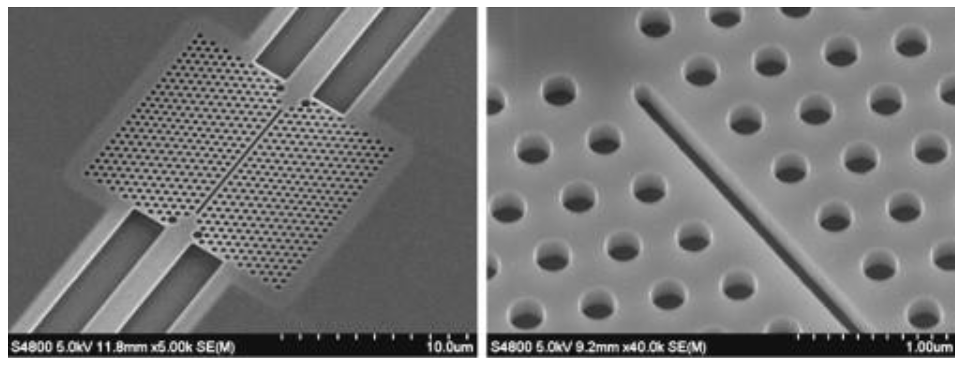
Figure 1. SEM pictures of SOI fabricated slotted PhC cavities [26].
Various parameters, including stability, sensitivity, selectivity, and limit of detection (LoD), are evaluated to assess the functioning of optical biosensors [27]. In the case of 2D PhC, sensitivity is determined by measuring the degree of contact between light and the immediate material. This parameter is usually stated as the slightest variation in resonance wavelength (λres) divided by the difference in medium RI in nanometers per refractive index unit (nm/RIU). Sensitivity is denoted as “S” and is expressed as
where Δλ and Δn are the changes in λres and RI of the ambient medium, respectively. Selectivity is important for the biosensor to identify specific analytes in a sample. The stability of the biosensor is influenced by the surrounding medium, and LoD is used to compare the performance of different optical biosensors. The LoD is generally defined as the minimum possible variation in the RI essential to producing a noticeable adjustment in the output signal.
Researchers worldwide are conducting extensive investigations into RI sensing devices that are based on PhCs. This technology enables researchers to create optical WGs with low bending losses and extreme-low group velocity, which can be used to elaborate compact optical devices that modify the optical phase of signals passing through the WGs. One such device, the Mach-Zehnder interferometer (MZI), is particularly important as it can serve as a building module for further complex optical devices, for example, filters, demultiplexers, interleaves, modulators, switches, and gates [28][29]. In [30], the authors analyze the operation of an MZI that consists of two coupled-cavity WGs with unique lengths, designed in a two-dimensional PhC. The authors provide simulation results using an FDTD code that proves the theoretical analysis and addresses the key limits of the structure’s performance. These sensors have quite a few advantages, such as requiring minimal sample preparation without the need for fluorescence labeling and providing high sensitivity. The sensing mechanism detects changes in the RI of a bulk solution caused by the presence of chemical analytes. These sensors can be used to differentiate the concentrations of biochemical samples in both gaseous and aqueous environments. Furthermore, these sensing devices can measure the surface or volumetric density of molecules and proteins.
The sensitivity of resonant wavelengths of PhC membrane nanocavities to ambient RI is a key factor in (bio)chemical sensing. By understanding how the resonant wavelengths vary with changes in RI, these nanocavities can be used as extremely sensitive sensing devices for detecting and measuring the concentration of various chemicals and biomolecules. The authors in [31] investigated the potential of using PhC membrane nanocavities with integrated InAs quantum dots for (bio)chemical sensing. They used photoluminescence measurements to identify the resonances of different modes in various point-defect-type cavities. Their results showed that there are systematic trends of sensitivity variation with the degree of intersection of modes with the PhC holes, both within a cavity type and for varying cavity types. The highest sensitivity observed was around 300 nm/RIU, which occurred when the mode overlap with the holes was about 25% and the solution was completely infiltrated [31].
Gas sensing devices established on PhCs for the mid-infrared range have attracted attention due to their ability to identify trace gases and their potential for integration with other technologies. In these sensing devices, the PhC structure is designed to interact with specific gas molecules, causing a change in the resonant frequency of the PhC, which can be sensed and analyzed. The mid-infrared range is particularly useful for gas sensing because many gases have strong absorption features in this range, allowing for highly selective detection. The point-defect nanocavities established on Si planar PhC have been enhanced for sensing the RI of gases in the MIR wavelength zone [32]. By improving the radius and position of the air holes, the Q/V ratio for the point-defect PhC nanocavities can be strengthened, resulting in a high sensitivity of 270 nm/RIU and an LoD of 10−4 RIU for sensing the RI of gases.
The near-infrared spectral region is examined numerically for a heat sensor based on a dielectric PhC [33]. The schematic of the PhC-based thermal sensor is shown in Figure 2a,b. A WG layer is placed on a silicon dioxide substrate, and air holes are drilled through it for easier fabrication. A functional layer of polydimethylsiloxane biguanide polymer is placed on top to sense ambient temperature; the optical characteristics of this layer change as the temperature does. Design and numerical simulation are performed using MEEP, an open-source finite-difference time-domain program. The device delivers a sensitivity value in the range of 0.109 nm/°C and a figure of merit (FOM) of 0.045 °C for an ambient temperature range of 10 to 90 °C, for which the sensor’s performance is examined. The device can be suggested for a variety of thermal sensing applications due to its high temperature tolerance, benign chemical qualities, inexpensive material cost, and ease of integration with optical fiber [33].

The fabrication of PhC structures can be complex and expensive. It often requires specialized equipment and techniques, such as electron-beam lithography (EBL) or nanoimprint lithography (NIL), which can limit their widespread adoption. PhC sensors are typically designed to operate within a specific wavelength range [34][35]. This limited range restricts their applicability to specific sensing applications and may require different designs or structures for different sensing targets. This WG configuration can be sensitive to shifts in the surrounding environment, for example, temperature, humidity, and strain. These variations can affect the RI of the materials used in the PhC structure, leading to fluctuations in the sensor’s performance and accuracy. When used for biological sensing applications, PhC sensors may face challenges due to the interaction between the sensing surface and the biological samples. Biofouling, non-specific binding, and other surface effects can affect the sensor’s performance and accuracy. Moreover, integrating PhC sensors into existing systems or devices can be challenging due to their specialized fabrication requirements and unique optical properties. This limitation may hinder their adoption in certain applications where seamless integration is crucial. Despite these disadvantages, PhC-based sensors offer unique advantages such as high sensitivity, label-free detection, and the potential for miniaturization. Ongoing research and technological advancements aim to overcome these limitations and expand the practical use of these sensors in various fields.
3. Surface Plasmon Resonance (SPR) Based Sensing Devices
Plasmonics is the study of the behavior of plasmons, which are collective oscillations of free electrons in a metal. In particular, the interaction of light with the free electrons on the surface of a metal can result in the excitation of SPs, which are waves of electron density that propagate along the metal surface [36]. SPs are collective oscillations of free electrons that can be excited on the surface of a metal [37]. These oscillations can couple with photons, resulting in strong light-matter interactions that can be exploited for various purposes. Localized surface plasmon resonances (LSPRs) are SP types that occur in small metallic nanoparticles or structures [38]. When the frequency of incident light matches the natural frequency of the LSPR, it can excite collective oscillations of free electrons within the nanoparticle, leading to strong absorption and scattering of light. LSPRs are highly dependent on the nanoparticle’s size, shape, and material, as well as the surrounding medium, making them a valuable tool for sensing and spectroscopy applications. Propagating surface plasmon polaritons (PSPPs) are hybrid waves that arise from the coupling between the EM waves in a dielectric medium and the SPs on a metal surface [39]. When the incident light’s frequency matches the SP’s natural frequency, a surface wave is generated that propagates along the metal-dielectric interface. This wave can be restrained to a sub-wavelength scale, allowing for highly efficient light-matter interactions [40]. PSPPs are used in various applications, such as nanophotonic devices, plasmonic WGs, and surface-enhanced Raman spectroscopy (SERS) [41].
SPR is a powerful tool for studying the interaction of light with matter, particularly in the field of biosensing. When the frequency of the incident light matches the natural frequency of the SP, a resonance occurs, leading to an alteration in the RI near the metal surface. This change in RI can be spotted and quantified, allowing for the detection of biomolecules and other analytes that bind to the metal surface. Plasmonic materials exhibit strong interactions between their electrons and EM radiation in the visible to near-infrared spectral range [42]. These materials typically consist of metals such as gold, silver, or copper, which have a high electron density and can support the collective oscillation of electrons known as SPs. Plasmonic materials are of great interest in the field of nanotechnology because they allow for the manipulation and control of light on a nanoscale [43].
Plasmonic sensors have significant potential for various environmental research applications due to their unique properties and capabilities. They offer the potential for real-time and continuous monitoring of environmental parameters. Their high sensitivity, fast response time, and compatibility with miniaturization enable the deployment of portable and autonomous sensor systems. Plasmonic sensors can be integrated into networks or distributed sensor arrays to provide spatially resolved and comprehensive environmental data. Plasmonic sensors can be utilized for the detection and analysis of biological entities in environmental samples. For example, they can detect and quantify specific bacteria, viruses, or biomarkers indicative of environmental contamination or ecosystem health. Plasmonic biosensors can be combined with microfluidic systems for automated sample handling and analysis, enabling rapid and sensitive environmental bioassays [44].
Plasmonic sensors can detect and analyze a wide range of environmental contaminants, including pesticides, toxins, and chemical warfare agents. The high sensitivity and selectivity of plasmonic sensors allow for the identification and quantification of these contaminants, even at trace levels. This capability is essential for environmental risk assessment and remediation efforts. They can contribute to the monitoring and analysis of atmospheric pollutants, including volatile organic compounds (VOCs) and greenhouse gases [45]. The ability of plasmonic sensors to detect low concentrations of these gases can aid in air quality assessment, climate change studies, and the development of mitigation strategies.
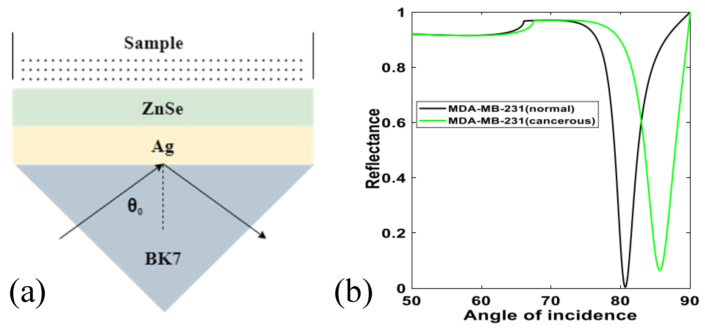
Prism-based SPR sensing devices are the most common type of SPR sensing device. These sensors use a thin metal film, typically made of gold or silver, coated onto a glass or prism surface. The metal film is often a few nanometers thick and is employed to excite SPs when light is directed onto it. When light is directed onto the prism, it is reflected off the metal film and interacts with the electron density at the metal surface. This interaction generates SPs, and the propagation of SPs is responsive to shifts in the RI of the medium near the metal surface. This makes SPR sensing devices useful for sensing changes in the concentration or binding of analytes near the metal surface. Prism-based SPR sensing devices are commonly used in different applications, including biomolecular interaction analysis, drug discovery, and environmental monitoring. They are extremely sensitive, label-free, and can be used to measure a broad range of analytes involving proteins, DNA, and small molecules. The detection of cancer and diabetes diseases is a crucial area of research in biosensing. To improve the accuracy of detection, researchers have introduced various methods, including the application of zinc selenide (ZnSe) semiconductor material to improve the sensitivity of a standard Ag-based SPR biosensor [46]. The suggested sensing device structure, as shown in Figure 3a is simple, economical, and simple to fabricate. In testing, the sensor detected various tumorous cells in human blood with an outstanding sensitivity of 359°/RIU and detected various glucose levels in human urine with high performance. The suggested biosensor can effectively sense distinct kinds of cancer cells and various concentrations of glucose in the urine, providing a promising avenue for disease detection. The reflection spectrum of the proposed sensor for normal MDA-MB-231 cells and cancerous cells is shown in Figure 3b. In [47], researchers proposed a sensitive prism-based SPR sensing device for sensing formalin via multilayer black phosphorous (BP). The study examines the impact of various materials on the sensor’s performance, including prism materials, metals, and 2D materials. The intended sensing device structure, consisting of BK7, silver, and nine layers of BP, achieves a sensitivity of 289.4565°/RIU and a detection accuracy (DA) of 0.3125/° for formalin detection.
Grating-coupled SPR sensors utilize a diffraction grating to couple incident light to the SP waves on a thin metal film. These sensors provide benefits over prism-based SPR sensors, including the ability to use lower-cost light sources, the ability to measure in a label-free and real-time manner, and the ability to perform multiplexed measurements. When the incident angle and wavelength match the plasmon resonance condition, a resonant coupling occurs between the incident light and the SPs, resulting in a dip in the reflected light intensity, which can be used to measure fluctuations in the RI of the metal film caused by the binding of molecules to its surface [48].
Highly efficient and compact SPR sensing devices are in high demand due to their versatility in various application scenarios when compared to traditional sensing devices. However, most compact SPR sensing devices require additional equipment like spectrometers or rotation stages to achieve high-precision spectral or angular analysis, leading to increased costs. A recent study demonstrates a low-cost and compact SPR sensor that utilizes a single grating as a coupler and a disperser [49]. The sensor utilizes a versatile digital disc-recordable disc grating to couple polychromatic light emitted from a light-emitting diode to SP modes. The same grating was used to disperse the light, which was then collected by a linear charge-coupled device. The sensor shows a high RI resolution of 5.52 × 10⁻⁵ RIU and can be employed in various fields, involving food safety, environmental examination, and medical diagnosis. A Si grating-enabled nanostructure for the sensing of RI using SPR phenomena in the NIR region is proposed [50]. The proposed structure exhibits sensitive behavior (1000 nm/RIU) for a specific range of analyte RI and accurate sensing behavior with an average quality factor value of 650 RIU−1.
Another type of SPR sensor is known as a WG-based SPR sensor, which uses a WG structure to excite SP waves on a thin metal film [51]. The sensing principle is established by the resonant coupling of the incident light with the SP waves. This dip can be used to measure the binding of molecules to the metal film surface, delivering knowledge about the concentration and affinity of the analyte molecules. WG-based SPR sensors offer several advantages, including the ability to achieve high sensitivity and selectivity, the ability to integrate with other on-chip components, and the potential for multiplexed measurements. A novel approach called a planar WG-based SPR sensing apparatus is suggested [52] using a silver-chloride material with a black phosphorus structure to sense formalin, a chemical used for food preservation that is linked to chronic cancer. The study examines the optimization of metal thickness and the chloride material’s optimal performance through transmittance power and resonance shift observations. The proposed sensing apparatus has a sensitivity of 344°/RIU, a quality factor of 166.99 RIU−1, a detection accuracy of 3.34, and a FOM of 164.74 [52]. The researchers proposed a novel WG-based SPR sensor consisting of graphene/Au/SiC layers that can work in the visible and NIR wavelength ranges [53]. The cross-sectional schematic of the sensor is explained in Figure 4. The sensitivity of the sensor was characterized, and the study showed that increasing the graphene layers improved the sensitivity. With 10 graphene layers, the sensor achieved a sensitivity of 2810 nm/RIU. The sensing apparatus has the potential for use in portable biosensors for various biological and chemical sensing applications [54].
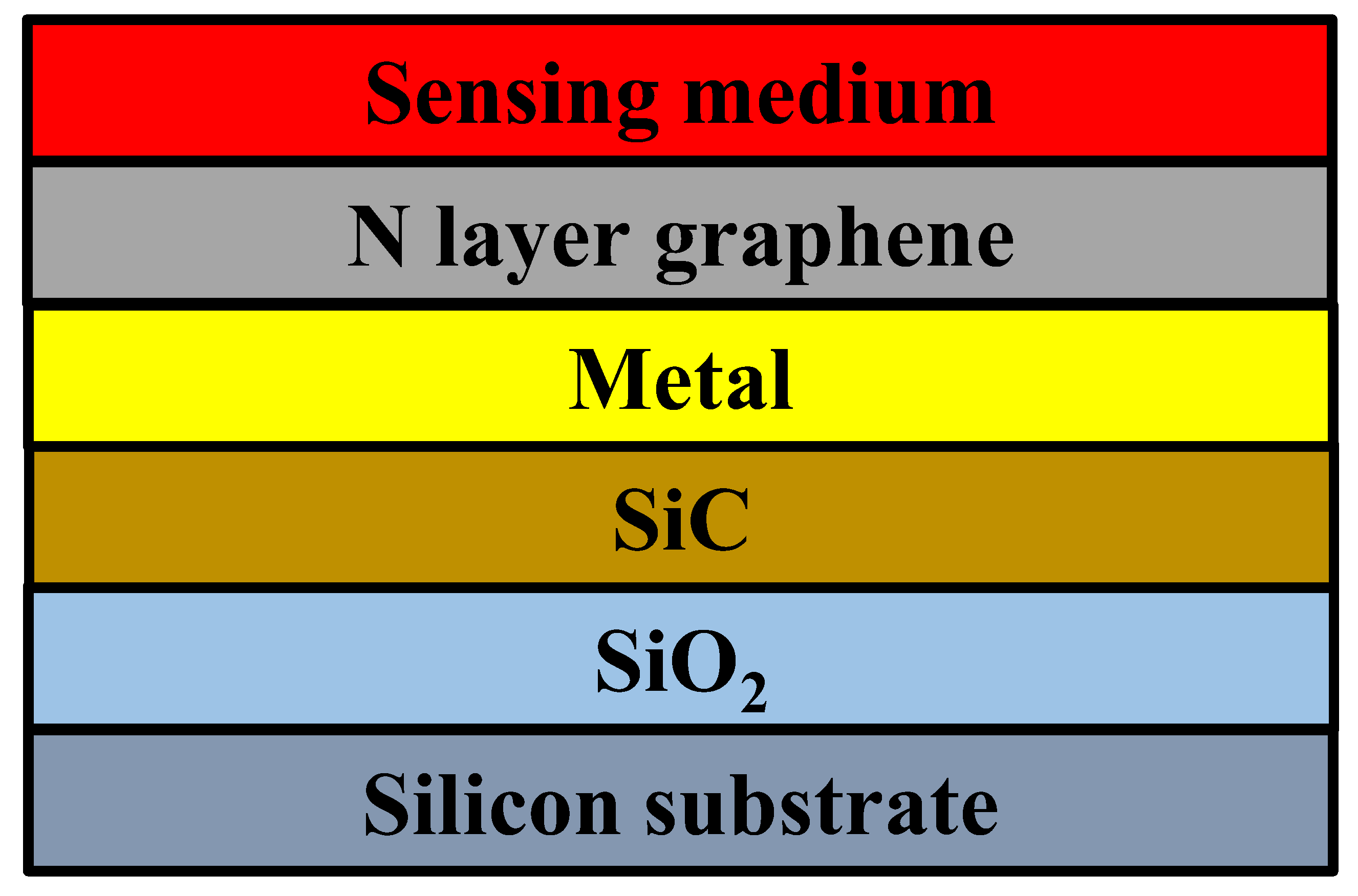
Figure 4. Cross-sectional schematic of the proposed graphene/Au/SiC WG SPR sensor structure. Inspired by [53].
Two-dimensional materials, such as graphene, transition metal dichalcogenides (TMDs), and black phosphorus, offer several advantages that can improve the sensitivity of sensors [55][56][57]. The ultrathin nature of 2D materials enables them to be placed near the sensing elements, resulting in improved sensitivity [58]. This proximity enhances the interaction between the analyte and the material, leading to a more sensitive detection or measurement. Two-dimensional materials possess an extremely high surface-to-volume ratio due to their atomic-thin structure. This large surface area allows for greater interaction with the surrounding environment, enhancing the chances of detecting and capturing analytes or signals [59]. Two-dimensional materials exhibit unique electrical properties that contribute to sensor sensitivity [60]. For instance, graphene is a highly conductive material, allowing for efficient charge transfer and electrical sensing. TMDs, on the other hand, possess a direct bandgap, enabling them to emit and absorb light efficiently, which is useful for optoelectronic sensing applications. Two-dimensional materials can be employed in a wide range of sensing modalities, including chemical, biological, and physical sensing. Their high sensitivity and diverse response to different stimuli make them suitable for detecting gases, biomolecules, strain, temperature, and much more [61].
Nanoparticle-enhanced SPR sensors are biosensors that incorporate nanoparticles into the SPR sensing process to improve the sensor’s sensitivity and selectivity. The nanoparticles function as signal amplifiers, providing a larger surface area for biomolecule immobilization and increasing the interface between the target analyte and the sensing surface. Different types of nanoparticles, such as gold, silver, silica, and magnetic particles, have been used in the development of nanoparticle-enhanced SPR sensors. A study was conducted to demonstrate the highly sensitive recognition of SARS-CoV-2 nucleocapsid protein (N protein) utilizing nanoparticle-enhanced SPR methods [62]. The research revealed that extremely sizeable gold nanoparticles (AuNPs) with diameters of hundreds of nm played a vital plasmonic role in extensively improving the limit of detection (LOD). The sensitivity of the SPR technique was improved by these large nanoparticles, resulting in the lowest LOD of SARS-CoV-2 N protein ever obtained, which was 85 fM [62].
Another study looked at the fundamental characteristics of the receptor-binding domain (RBD), a crucial part of the SARSCoV-2 spike protein that is essential for viral infection. Surface-enhanced Raman spectroscopy (SERS) using AuNPs was used to record the Raman modes of the SARS-CoV-2 RBD [63]. Because of the aggregation of AuNPs, the observed Raman increase is substantially wavelength-dependent. By using principal component analysis, it was possible to determine the function of secondary structures in the SERS process, which is supported by thermal stability during laser heating. The distinctive Raman spectra of RBDs from SARS-CoV-2 and MERS-CoV were examined. Using machine learning methods, the Raman spectra of two RBDs can be readily differentiated with accuracy, precision, recall, and F1 scores all over 95%. In-depth knowledge of the SARS-CoV-2 RBD is provided by this work, which also lays the path for quick analysis and differentiation of complex proteins of infectious viruses and other macromolecules [63].
Plasmonic sensors often require precise control over the size, shape, and arrangement of metallic nanostructures to achieve the desired plasmonic properties. Fabrication techniques such as EBL or FIB milling are commonly employed but can be time-consuming, expensive, and challenging to scale up for large-area sensing devices [34]. Plasmonic sensors typically rely on metallic nanoparticles or thin films, such as gold or silver, which exhibit strong plasmonic resonances in the visible or infrared range. However, these metals may not be compatible with certain environments or specific sensing applications. For example, they may corrode in harsh chemical environments or be unsuitable for biological sensing due to their cytotoxicity. Choosing the right substrate is crucial for plasmonic sensors [15]. The substrate should be optically transparent in the spectral range of interest to enable efficient coupling of light with the plasmonic structures [64]. Additionally, the substrate should have low autofluorescence and minimal interaction with the analyte being sensed. Identifying suitable substrates that meet these criteria can be challenging. Plasmonic sensors are often exposed to various environmental factors, such as temperature variations, humidity, and chemical interactions. These factors can degrade the performance and stability of the plasmonic structures over time. Ensuring the long-term stability and reliability of plasmonic sensors remains a significant challenge. Achieving high fabrication yield and reproducibility is crucial for commercializing plasmonic sensors. The nanoscale nature of these devices makes them sensitive to fabrication variations, leading to inconsistent performance across different devices. Developing reliable fabrication processes and quality control measures is essential to addressing this challenge. Plasmonic sensors often need to be integrated with other components, such as light sources, detectors, and microfluidic systems, to form complete sensing platforms [65][66]. Ensuring seamless integration while maintaining the sensor’s performance and scalability can be complex and require interdisciplinary expertise. Addressing these fabrication challenges is essential to harnessing the full potential of plasmonic sensors and enabling their widespread adoption in various fields, including biomedical diagnostics, environmental monitoring, and industrial applications [67]. Ongoing research efforts aim to develop innovative fabrication techniques, explore new materials, and enhance the stability and reliability of plasmonic sensors to overcome these challenges [68].
References
- Butt, M.; Voronkov, G.; Grakhova, E.; Kutluyarov, R.; Kazanskiy, N.; Khonina, S. Environmental Monitoring: A Compre-hensive Review on Optical Waveguide and Fiber-Based Sensors. Biosensors 2022, 12, 1038.
- Arano-Martinez, J.; Martinez-Gonzalez, C.; Salazar, M.; Torres-Torres, C. A framework for biosensors assisted by mul-tiphoton effects and machine learning. Biosensors 2022, 12, 710.
- Kazanskiy, N.L.; Khonina, S.N.; Butt, M.A. Recent Development in Metasurfaces: A Focus on Sensing Applications. Nanomaterials 2022, 13, 118.
- Irfan, M.; Khan, Y.; Rehman, A.U.; Butt, M.A.; Khonina, S.N.; Kazanskiy, N.L. Plasmonic Refractive Index and Temperature Sensor Based on Graphene and LiNbO3. Sensors 2022, 22, 7790.
- Daher, M.G.; Taya, S.A.; Colak, I.; Vigneswaran, D.; Olaimat, M.M.; Patel, S.K.; Ramahi, O.M.; Almawgani, A.H. Design of a nano-sensor for cancer cell detection based on a ternary photonic crystal with high sensitivity and low detection limit. Chin. J. Phys. 2022, 77, 1168–1181.
- Wu, R.; Biondi, A.; Cao, L.; Gandhi, H.; Abedin, S.; Cui, G.; Yu, T.; Wang, X. Composite Bridge Girders Structure Health Monitoring Based on the Distributed Fiber Sensing Textile. Sensors 2023, 23, 4856.
- Nowak, S.; Sherizadeh, T.; Esmaeelpour, M.; Guner, D.; Karadeniz, K.E. Hybrid Fiber Optic Cable for Strain Profiling and Crack Growth Measurement in Rock, Cement, and Brittle Installation Media. Sensors 2022, 22, 9685.
- Yuan, B.; Ying, Y.; Morgese, M.; Ansari, F. Theoretical and Experimental Studies of Micro-Surface Crack Detections Based on BOTDA. Sensors 2022, 22, 3529.
- Png, W.H.; Lin, H.S.; Pua, C.H.; Abd Rahman, F. Pipeline monitoring and leak detection using Loop integrated Mach Zehnder Inter-ferometer optical fiber sensor. Opt. Fiber Technol. 2018, 46, 221–225.
- Khonina, S.; Voronkov, G.; Grakhova, E.; Kazanskiy, N.; Kutluyarov, R.; Butt, M. Polymer Waveguide-Based Optical Sen-sors—Interest in Bio, Gas, Temperature, and Mechanical Sensing Applications. Coatings 2023, 13, 549.
- Zhirnov, A.A.; Chesnokov, G.Y.; Stepanov, K.V.; Gritsenko, T.V.; Khan, R.I.; Koshelev, K.I.; Chernutsky, A.O.; Svelto, C.; Pnev, A.B.; Valba, O.V. Fiber-Optic Telecommunication Network Wells Monitoring by Phase-Sensitive Optical Time-Domain Reflectometer with Disturbance Recognition. Sensors 2023, 23, 4978.
- Zahir, M.H.M.; Aziz, K.M.A.; Ghazali, A.R.; Latiff, A.H.A. Effectiveness of Fiber Optic Distributed Acoustic Sensing (DAS) in Vertical Seismic Profiling (VSP) Field Survey. Appl. Sci. 2023, 13, 5002.
- Weiss, M.; Srivastava, R.; Groger, H.; Lo, P.; Luo, S.-F. A theoretical investigation of environmental monitoring using sur-face plasmon resonance waveguide sensors. Sens. Actuators A Phys. 1996, 51, 211–217.
- Kazanskiy, N.; Khonina, S.; Butt, M. Polarization-insensitive hybrid plasmonic waveguide design for evanescent field ab-sorption gas sensor. Photonic Sens. 2021, 11, 279–290.
- Butt, M.A. Numerical Assessment of a Metal-Insulator-Metal Waveguide-Based Plasmonic Sensor System for the Recognition of Tuberculosis in Blood Plasma. Micromachines 2023, 14, 729.
- Butt, M.; Khonina, S.; Kazanskiy, N. 2D-Photonic crystal heterostructures for the realization of compact photonic devices. Photonics Nanostruct.-Fundam. Appl. 2021, 44, 100903.
- Butt, M.; Khonina, S.; Kazanskiy, N. Recent advances in photonic crystal optical devices: A review. Opt. Laser Technol. 2021, 142, 107265.
- Yang, D.; Wang, X.; Tian, H.; Ji, Y. Electro-optic modulation property of slow light in coupled photonic crystal resonator arrays. Opt. Appl. 2011, 41, 753–763.
- Chen, Y.; Dong, J.; Liu, T.; Zhu, Q.; Chen, W. Refractive index sensing performance analysis of photonic crystal containing graphene based on optical Tamm state. Mod. Phys. Lett. B 2016, 30, 1650030.
- Poonguzhali, S.; Sivasangari, A.; Ajitha, P.; Lalithakumari, S.; Sridevi, A.; Danasegaran, S.K. Design and performance analysis of smart photonic sensors for industrial applications. Curr. Appl. Phys. 2022, 39, 183–189.
- Rodriguez, G.A.; Markov, P.; Cartwright, A.P.; Choudhury, M.H.; Afzal, F.O.; Cao, T.; Halimi, S.I.; Retterer, S.T.; Kravchenko, I.I.; Weiss, S.M. Photonic crystal nanobeam biosensors based on porous silicon. Opt. Express 2019, 27, 9536–9549.
- Fan, S.; Joannopoulos, J.D. Analysis of guided resonances in photonic crystal slabs. Phys. Rev. B 2002, 65, 235112.
- Khani, S.; Hayati, M. Optical biosensors using plasmonic and photonic crystal band-gap structures for the detection of basal cell cancer. Sci. Rep. 2022, 12, 5246.
- Chen, W.; Long, K.; Lu, M.; Chaudhery, V.; Yu, H.; Choi, J. Photonic crystal enhanced microscopy for imaging of live cell adhesion. Analyst 2013, 138, 5886–5894.
- Zhou, Y.; Hu, H.; Chen, W.; Lu, M.; Tian, L.; Yu, H. Single nanoparticle detection using photonic crystal enhanced micros-copy. Analyst 2014, 139, 1007–1015.
- Scullion, M.; Falco, D.; Krauss, T. Slotted photonic crystal cavities with integrated microfludics for biosensing applications. Biosens. Bioelectron. 2011, 27, 101–105.
- Kazanskiy, N.; Khonina, S.; Butt, M. Plasmonic sensors based on Metal-insulator-metal waveguides for refractive index sensing applications: A brief review. Phys. E Low-Dimens. Syst. Nanostruct. 2019, 117, 113798.
- Kamada, S.; Okamoto, T.; El-Zohary, S.E.; Haraguchi, M. Design optimization and fabrication of Mach-Zehnder interfer-ometer based on MIM plasmonic waveguides. Optics Express 2016, 24, 16224–16231.
- Guan, X.; Wang, X.; Frandsen, L.H. Optical temperature sensor with enhanced sensitivity by employing hybrid waveguides in a silicon Mach-Zehnder interferometer. Opt. Express 2016, 24, 16349–16356.
- Martínez, A.; Sanchis, P.; Marti, J. Mach–Zehnder interferometers in photonic crystals. Opt. Quantum Electron. 2005, 37, 77–93.
- Dündar, M.A.; Ryckebosch, E.C.; Nötzel, R.; Karouta, F.; Van Ijzendoorn, L.J.; Van Der Heijden, R.W. Sensitivities of InGaAsP photonic crystal membrane nanocavities to hole refractive index. Opt. Express 2010, 18, 4049–4056.
- Kassa-Baghdouche, L.; Cassan, E. Mid-infrared gas sensor based on high-Q/V point-defect photonic crystal nanocavities. Opt. Quantum Electron. 2020, 52, 260.
- Khan, Y.; Butt, M.A.; Khonina, S.N.; Kazanskiy, N.L. Thermal Sensor Based on Polydimethylsiloxane Polymer Deposited on Low-Index-Contrast Dielectric Photonic Crystal Structure. Photonics 2022, 9, 770.
- Broers, A.N. Resolution limits for electron-beam lithography. IBM J. Res. Dev. 1988, 32, 502–513.
- Manfrinato, V.R.; Zhang, L.; Su, D.; Duan, H.; Hobbs, R.G.; Stach, E.A.; Berggren, K.K. Resolution Limits of Electron-Beam Lithography toward the Atomic Scale. Nano Lett. 2013, 13, 1555–1558.
- Lai, R.; Shi, P.; Yi, Z.; Li, H.; Yi, Y. Triple-Band Surface Plasmon Resonance Metamaterial Absorber Based on Open-Ended Prohibited Sign Type Monolayer Graphene. Micromachines 2023, 14, 953.
- Butt, M. Numerical investigation of a small footprint plasmonic Bragg grating structure with a high extinction ratio. Photon. Lett. Pol. 2020, 12, 82–84.
- Butt, M.; Khonina, S.; Kazanskiy, N. A plasmonic colour filter and refractive index sensor applications based on metal–insulator–metal square µ-ring cavities. Laser Phys. 2020, 30, 016205.
- Zhang, Z.; Fang, Y.; Wang, W.; Chen, L.; Sun, M. Propagating Surface Plasmon Polaritons: Towards Applications for Re-mote-Excitation Surface Catalytic Reactions. Adv. Sci. 2016, 3, 1500215.
- Butt, M.; Kazanskiy, N.; Khonina, S. Tapered waveguide mode converters for metal-insulator-metal waveguide plasmonic sensors. Measurement 2023, 211, 112601.
- Moretti, L.; Mazzanti, A.; Rossetti, A.; Schirato, A.; Polito, L.; Pizzetti, F.; Sacchetti, A.; Cerullo, G.; Della Valle, G.; Rossi, F.; et al. Plasmonic control of drug release efficiency in agarose gel loaded with gold nanoparticle assemblies. Nanophotonics 2021, 10, 247–257.
- Bellassai, N.; D’Agata, R.; Jungbluth, V.; Spoto, G. Surface plasmon resonance for biomarker detection: Advances in non-invasive cancer diagnosis. Front. Chem. 2019, 7, 570.
- Anwar, R.S.; Ning, H.; Mao, L. Recent advancements in surface plasmon polaritons-plasmonics in subwavelength structures in microwave and terahertz regimes. Digit. Commun. Netw. 2018, 4, 244–257.
- Mauriz, E. Recent progress in plasmonic biosensing schemes for virus detection. Sensors 2020, 20, 4745.
- Pathak, A.; Viphavakit, C. VOC Biomarker Monitoring for Diabetes Through Exhaled Breath Using Ag/P-TiO2 Composite Plasmonic Sensor. IEEE Sens. J. 2021, 21, 22631–22637.
- El-assar, M.; Taha, T.; El-Samie, F.; Fayed, H.; Aly, M. ZnSe-based highly-sensitive SPR biosensor for detection of different cancer cells and urine glucose levels. Opt. Quantum Electron. 2022, 55, 76.
- Kumari, A.; Vyas, V.; Kaur, B.; Kaushik, B.K.; Kumar, S. Black phosphorous-based highly sensitive surface plasmonic sensor for detection of formalin. IEEE Trans. Plasma Sci. 2023, 51, 140–147.
- Long, S.; Cao, J.; Wang, Y.; Gao, S.; Xu, N.; Gao, J.; Wan, W. Grating coupled SPR sensors using off the shelf compact discs and sensitivity dependence on grating period. Sens. Actuators Rep. 2020, 2, 100016.
- Wang, E.; Cao, J.; Cao, K.; Xu, N.; Zhu, H. Compact surface plasmon resonance sensor using the digital versatile disc grat-ing as a coupler and a disperser. Opt. Eng. 2023, 62, 017105.
- Pandey, A.K.; Kumar, H. Quality factor enhanced plasmonic grating sensor in the near infrared region of application. Opt. Quantum Electron. 2022, 55, 57.
- Feiler, M.; Ziman, M.; Kovac, J.; Kuzma, A.; Uherek, F. Design of Optimal SPR-Based Multimode Waveguide Sensor for a Wide Range of Liquid Analytes. Photonics 2023, 10, 618.
- Vasimalla, Y.; Singh, L. Design and analysis of planar waveguide-based spr sensor for formalin detection using Ag-Chloride-Bp structure. IEEE Trans. NanoBiosci. 2023, 22, 365–374.
- Du, W.; Miller, L.; Zhao, F. Numerical Study of Graphene/Au/SiC Waveguide-Based Surface Plasmon Resonance Sensor. Biosensors 2021, 11, 455.
- Chen, S.; Wang, J.; Zhang, C.; Li, M.; Li, N.; Wu, H.; Liu, Y.; Peng, W.; Song, Y. Marine Structural Health Monitoring with Optical Fiber Sensors: A Review. Sensors 2023, 23, 1877.
- Ye, Z.; Wu, P.; Wang, H.; Jiang, S.; Huang, M.; Lei, D.; Wu, F. Multimode tunable terahertz absorber based on a quarter gra-phene disk structure. Results Phys. 2023, 48, 106420.
- Shangguan, Q.; Chen, Z.; Yang, H.; Cheng, S.; Yang, W.; Yi, Z.; Wu, X.; Wang, S.; Yi, Y.; Wu, P. Design of ultra-narrow band graphene refractive index sensor. Sensors 2022, 22, 6483.
- Jia, Z.; Huang, L.; Su, J.; Tang, B. Tunable Electromagnetically Induced Transparency-Like in Graphene metasurfaces and its Application as a Refractive Index Sensor. J. Light. Technol. 2020, 39, 1544–1549.
- Xia, G.; Zhou, C.; Jin, S.; Huang, C.; Xing, J.; Liu, Z. Sensitivity enhancement of two-dimensional materials based on genetic optimization in surface plasmon resonance. Sensors 2019, 19, 1198.
- Sulleiro, M.; Dominguez-Alfaro, A.; Alegret, N.; Silvestri, A.; Gomez, I. 2D materials towards sensing technology: From fun-damentals to applications. Sens. Bio-Sens. Res. 2022, 38, 100540.
- Shi, S.; Hu, R.; Wu, E.; Li, Q.; Chen, X.; Guo, W.; Sun, C.; Hu, X.; Zhang, D.; Liu, J. Highly-sensitive gas sensor based on two-dimensional material field effect transistor. Nanotechnology 2018, 29, 435502.
- Tyagi, D.; Wang, H. Recent advances in two-dimensional-material-based sensing technology toward health and environ-mental monitoring applications. Nanoscale 2020, 12, 3535–3559.
- Yano, T.-A.; Kajisa, T.; Ono, M.; Miyasaka, Y.; Hasegawa, Y.; Saito, A. Ultrasensitive detection of SARS-CoV-2 nucleocapsid protein using large gold nanoparticle-enhances surface plasmon resonance. Sci. Rep. 2022, 12, 1060.
- Zhang, K.; Wang, Z.; Liu, H.; Perea-López, N.; Ranasinghe, J.C.; Bepete, G.; Minns, A.M.; Rossi, R.M.; Lindner, S.E.; Huang, S.X.; et al. Thermal stability of the SARS-CoV-2 receptor-binding domain using surface-enhanced raman scattering and machine learning. ACS Photon. 2022, 9, 2963–2972.
- Kazanskiy, N.L.; Khonina, S.N.; Butt, M.A. A Review of Photonic Sensors Based on Ring Resonator Structures: Three Widely Used Platforms and Implications of Sensing Applications. Micromachines 2023, 14, 1080.
- Butt, M.; Kazanskiy, N.; Khonina, S. On-chip symmetrically and asymmetrically transformed plasmonic Bragg grating formation loaded with a functional polymer for filtering and CO2 gas sensing applications. Measurement 2022, 201, 111694.
- Butt, M.A.; Kazanskiy, N.L.; Khonina, S.N. Miniaturized Design of a 1 × 2 Plasmonic Demultiplexer Based on Metal–Insulator-Metal Waveguide for Telecommunication Wavelengths. Plasmonics 2023, 18, 635–641.
- Dahlin, A.; Wittenberg, N.; Hook, F.; Oh, S.-H. Promises and challenges of nanoplasmonic devices for refractometric bio-sensing. Nanophotonics 2023, 2, 83–101.
- Duan, H.; Wang, T.; Su, Z.; Pang, H.; Chen, C. Recent progress and challenges in plasmonic nanomaterials. Nanotechnol. Rev. 2022, 11, 846–873.
More
Information
Subjects:
Others
Contributors
MDPI registered users' name will be linked to their SciProfiles pages. To register with us, please refer to https://encyclopedia.pub/register
:
View Times:
1.2K
Revisions:
2 times
(View History)
Update Date:
28 Jun 2023
Table of Contents


Notice
You are not a member of the advisory board for this topic. If you want to update advisory board member profile, please contact office@encyclopedia.pub.
OK
Confirm
Only members of the Encyclopedia advisory board for this topic are allowed to note entries. Would you like to become an advisory board member of the Encyclopedia?
Yes
No
${ textCharacter }/${ maxCharacter }
Submit
Cancel
Back
Comments
${ item }
|
${ item.createdUser.fullName }
${ item.createdAt }
${ item.vote }
${ item.reply }
Delete
${ reply.createdUser.fullName }
${ reply.createdAt }
${ reply.vote }
Delete
There is no reply to this comment~
${ item.replyTextCharacter }/${ item.replyMaxCharacter }
Submit
Cancel
More
No more~
There is no comment~
${ textCharacter }/${ maxCharacter }
Submit
Cancel
${ selectedItem.replyTextCharacter }/${ selectedItem.replyMaxCharacter }
Submit
Cancel
Confirm
Are you sure to Delete?
Yes
No