Your browser does not fully support modern features. Please upgrade for a smoother experience.
Submitted Successfully!
 +1 credit
Thank you for your contribution! You can also upload a video entry or images related to this topic.
For video creation, please contact our Academic Video Service.
| Version | Summary | Created by | Modification | Content Size | Created at | Operation |
|---|---|---|---|---|---|---|
| 1 | Dieter Bimberg | -- | 2876 | 2023-04-12 07:36:57 | | | |
| 2 | Jason Zhu | -1 word(s) | 2875 | 2023-04-13 04:56:13 | | |
Video Upload Options
We provide professional Academic Video Service to translate complex research into visually appealing presentations. Would you like to try it?
Cite
If you have any further questions, please contact Encyclopedia Editorial Office.
Tian, S.; Ahamed, M.; Bimberg, D. Short Wavelength Energy-Efficient High-Speed Vertical-Cavity Surface-Emitting Lasers. Encyclopedia. Available online: https://encyclopedia.pub/entry/42968 (accessed on 11 June 2026).
Tian S, Ahamed M, Bimberg D. Short Wavelength Energy-Efficient High-Speed Vertical-Cavity Surface-Emitting Lasers. Encyclopedia. Available at: https://encyclopedia.pub/entry/42968. Accessed June 11, 2026.
Tian, Si-Cong, Mansoor Ahamed, Dieter Bimberg. "Short Wavelength Energy-Efficient High-Speed Vertical-Cavity Surface-Emitting Lasers" Encyclopedia, https://encyclopedia.pub/entry/42968 (accessed June 11, 2026).
Tian, S., Ahamed, M., & Bimberg, D. (2023, April 12). Short Wavelength Energy-Efficient High-Speed Vertical-Cavity Surface-Emitting Lasers. In Encyclopedia. https://encyclopedia.pub/entry/42968
Tian, Si-Cong, et al. "Short Wavelength Energy-Efficient High-Speed Vertical-Cavity Surface-Emitting Lasers." Encyclopedia. Web. 12 April, 2023.
Copy Citation
Vertical-cavity surface-emitting lasers (VCSELs) were becoming the dominating optical sources for data communication in such centers for all distances and wavelengths. VCSELs are of low production cost, can be tested on-wafer, and enable low energy consumption. 850 nm multi-mode VCSELs are widely used for the optical links inside data centers and supercomputers, together with multi-mode fibers. Long-wavelength single-mode VCSELs (1310 nm or 1550 nm) based on InP extend the transmission distance and enable wavelength division multiplexing (WDM) technologies.
vertical-cavity surface-emitting lasers (VCSELs)
high speed
energy efficiency
1. Introduction
Internet traffic increases by approximately 60% per year, much more than predicted from 2017 to 2022, 6 years ago [1]. Novel or more rapidly than expected expanding consumer and social media applications, such as Netflix and Block Chain, are responsible for this growth. The electrical power and cooling demands inside data centers are thus exploding. The introduction of 5G and the transition to 6G and the use of artificial intelligence (AI) and automotive applications will lead to further significant increases in the number, size, and power consumption of data centers.
Vertical-cavity surface-emitting lasers (VCSELs) were becoming the dominating optical sources for data communication in such centers for all distances and wavelengths. VCSELs are of low production cost, can be tested on-wafer, and enable low energy consumption [2]. Presently, 850 nm multi-mode VCSELs are widely used for the optical links inside data centers and supercomputers, together with multi-mode fibers [3][4][5]. Long-wavelength single-mode VCSELs (1310 nm or 1550 nm) based on InP extend the transmission distance and enable wavelength division multiplexing (WDM) technologies.
GaAs-based VCSELs exhibit low threshold currents, large quantum efficiency, modulation frequencies up to 30 GHz, and a bit rate dependent on energy consumption [6]. An increase of line rates under non-return-to-zero on-off keying (NRZ-OOK) modulation and 4-level pulse amplitude modulation (PAM 4), including pre-emphasis, were demonstrated [7][8][9]. Using WDM, the optical link capacity can be greatly increased [10]. Low threshold currents and a large slope efficiency due to the small cavity volume, enables data transmission with a dissipated heat energy per bit of 56 fJ at a bit rate of 25 Gb/s [11]. The present challenge is to achieve data transmission rates of 400 Gb/s and beyond at an energy per bit still less than 100 fJ/bit, for both short and long distances [12].
2. Energy-Efficient High-Speed Short-Wavelength VCSELs
2.1. 850 nm VCSELs
Presently, 850 nm MM VCSELs are the main light source for short distance optical interconnects (less than 300 m) because of their low cost. In early work, unstrained GaAs QWs with AlGaAs barrier layers were used for 850 nm high-speed VCSELs. In more recent work, strained InGaAs QWs were adopted because of their larger differential gain, compared to unstrained GaAs QWs. Many groups have realized up to an approximate 30 GHz modulation bandwidth of 850 nm VCSELs, by using strained InGaAs QWs, in combination with graded interfaces and modulation doped DBRs, multiple oxide apertures, a short cavity, and photon lifetime tuning [13][14][15]. Under both NRZ-OOK (PAM 2) and PAM 4 modulation, the bit rates for short distances have been increased beyond 50 Gb/s or 100 Gb/s, respectively. Larger link capacities are achieved using feed-forward equalization (FFE) [8][16].
Bimberg’s group realized the largest bit rates for error-free data transmission combined with the lowest energy consumption for 850 nm VCSELs [11][17]. The VCSEL was formed by 21 pairs of p-doped Al0.12Ga0.88As/Al0.90Ga0.10As top DBR, 33.5 pairs of n-doped Al0.12Ga0.88As/Al0.90Ga0.10As bottom DBR and an active region of five 12-monolayers-thick strained In38Ga62As QWs, surrounded by Al0.45Ga0.55As barrier layers. Multiple oxide layers were employed to reduce the capacitance of the VCSEL. Compared to the design in Refs. [18][19], this design has a larger mole fraction of indium, thinner QWs, and a thinner overall active area. This approach is beneficial to reduce the transit time, suppress vertical carrier leakage, increase the confinement of photons in the cavity, and thus improve the modulation response. Modulation doping was adopted throughout both DBRs to minimize the absorption losses and increase the efficiency. A highly p-doped GaAs phase-offset layer was added on the topmost DBR to act as a low contact resistance layer in addition to a photon lifetime tuning layer.
For VCSELs with oxide-aperture diameters of 3.5 μm, error-free data transmission at 25 Gb/s with the record low EDR of 77 fJ/bit and HBR of 56 fJ/bit was realized [11][17]. The current density for achieving a 25-Gb/s operation was below 10 kA/cm2, demonstrating the suitability of such devices for applications in highly reliable commercial OI systems. Larger bit rates were achieved based on the same design. For 40 Gb/s, an HBR of 108 fJ/bit was demonstrated [20]. Error-free data transmission at 30 Gb/s across 500 m of MMF was realized with an HBR of 85 fJ/bit. Additionally, at 25 Gb/s across 1000 m of MMF, an HBR of 100 fJ/bit was demonstrated [13]. It was demonstrated that the smaller oxide-aperture-diameters VCSELs are more energy efficient than the ones with larger aperture diameters, due to the large D-factor of the small oxide aperture.
Alternatively to oxide apertures, Zn-diffusion and oxide-relief techniques were reported to be successful in Ref. [21].
2.2. 980 nm and 1060 nm VCSELs
High-speed VCSELs with wavelengths from 980 to 1100 nm have attracted a lot of attention recently, although they are not yet included in the standards of IEEE [22]. Compared with 850 nm high-speed VCSELs, devices emitting at longer wavelengths benefit from lower chromatic dispersion and lower transmission loss in MMF, and a larger temperature insensitivity of the quantum efficiency, due to reduced carrier spill-out of the well. Again, strained InGaAs QWs (or QDs) can be used to create emissions from 980 to 1100 nm. These QWs show a larger differential gain and lower transparency carrier density, allowing a larger D factor, and in turn, a larger modulation bandwidth. Work on high bit rate NRZ-OOK data transmission in MMF links was carried out for 980 to 1100 nm VCSELs [23][24][25][26][27][28][29]. At 980 nm, the TU Berlin group demonstrated a 46 Gb/s NRZ-OOK data transmission at 85 °C [25]. By optimizing the photon lifetime of 980 nm VCSELs, Larisch et al. increased the data rate to 50 + Gb/s at 85 °C [23], a number limited then by the measurement set-up.
Li et al., from Bimberg’s group, realized error-free data transmission at 38 Gb/s at 85 °C, with a record low HBR of 177 fJ/bit by using 980 nm VCSELs [24]. The active region of the VCSEL was formed by five 4.2 nm-thick compressively strained In0.21Ga0.79As QWs surrounded by 6 nm GaAs0.12P0.88 partially strained compensating barrier layers. The optical cavity thickness is 1.5λ. A 15 nm QW gain-to-etalon wavelength offset was used to improve the VCSEL temperature stability, as well as to enable energy-efficient operation at high temperatures. Across the entire temperature range, the modulation peak-to-peak voltage was kept unchanged. In addition, temperature-stable energy dissipation was realized.
This design was improved later and a larger bit rate of 46 Gb/s was achieved at 85 °C. Compared with the previous design, the optical cavity thickness was reduced to λ/2 to increase the photon density at the QWs. Five compressively strained 4 nm-thick In0.22Ga0.78As QWs with 5.1 nm-thick tensile-strained GaAs0.9P0.1 barrier layers partially compensating the QW layer strain formed the active region. A total of 21.5 pairs of p-doped GaAs/Al0.90Ga0.10As top DBR and 35 pairs of n-doped bottom DBR mirrors, both including modulation-doped current spreading layers, were designed. Two 20 nm-thin oxide apertures, which were formed by the selective wet oxidation of Al0.98Ga0.02As layers, were used for optical and current confinement. Additional GaAs layers were added to the topmost DBR for the purpose of the photon lifetime tuning. Error-free operation at 50 Gb/s at 25 °C was achieved for the 5 μm oxide-aperture diameter VCSELs. At this bit rate, the HBR was 302 fJ/bit, which was lower than the value of 340 fJ/bit for 850 nm VCSELs. Error-free operation at 46 Gb/s at 85 °C was also achieved, due to a 16 nm QW gain-to-etalon wavelength offset [25].
Simpanen et al. realized energy-efficient high-speed 1060 nm VCSEL using a design derived from their previous 850 nm VCSEL [26]. Five strained InGaAs QWs were used as the active region to achieve high differential gain. A half-wavelength-thick short cavity was used for large longitudinal optical confinement. Twenty Al0.9Ga0.1As/GaAs top p-doped DBRs with modulation-doped and parabolically graded compositional intermediate layers were adopted to have a low resistance and optical loss. Five pairs of Al0.9Ga0.1As/GaAs and 24 pairs of AlAs/GaAs bottom n-DBRs with modulation-doped and step-graded compositional intermediate were shown to have a low thermal impedance. Multiple oxide apertures were in the top DBR. The two primary oxide apertures provided transverse optical and current confinement, and the other four secondary oxide apertures reduced the capacitance. By using 4 μm oxide apertures, HDRs of 100 fJ/bit at 50 Gb/s NRZ-OOK modulation was reported for 1060 nm VCSELs.
Excellent energy efficiency for high-speed 1060 nm VCSELs was also achieved by Furukawa [27]. Oxide-confined double intra-cavity structures are used here. Compressively strained InGaAs QWs provided high differential gain. Undoped semiconductor bottom-DBR and dielectric top-DBR were used, leading to low internal optical loss. For 5 μm aperture VCSELs, a power dissipation of 76 fJ/bit at 25 Gb/s and 2 mA bias current was demonstrated.
3. Adapt Photon Lifetime of VCSELs to Data Rate
In previous work, the impact of photon lifetime tuning on the performance of high-speed VCSELs was investigated. By etching the GaAs layer of the topmost DBR, the mirror loss was increased, thus the photon lifetime and the damping became smaller. Therefore, at a given electrical power, Pel, the VCSEL with an etched DBR achieved a larger f3dB, compared with VCSELs without etched DBR. These results indicated that photon lifetime tuning does not only improve the static performance, such as the maximum output power, but can also improve the energy efficiency of the VCSEL [23], where SiN was deposited on top of the surface, instead of etching.
The tuning of the photon lifetime and damping of any VCSEL can be realized with large precision by the homogeneous deposition of SiN on the top layer, which can be better controlled than etching. The output power and the cut-off frequency of the VCSEL can be increased [30], and the energy consumption can be decreased by adapting the photon lifetime. The modulation current efficiency factor has been determined experimentally based on large signal measurement results marked with (a) and (c) for both photon lifetimes [23][25]. At 50 Gb/s, by using the VCSEL with long photon lifetime (large damping), the EDR is 530 fJ/bit, while by using the VCSEL with a short photon lifetime (small damping), the EDR is only 400 fJ/bit. Therefore, a 25% reduction of EDR is achieved for a 50 Gb/s data transmission by choosing the optimum photon lifetimes of the VCSELs. In addition, a crossover between the two curves is observed. The grey dashed line passing through the crossing divides the two curves into two sections. From an energy-consumption point or view, it is preferable to fabricate VCSELs with a short photon lifetime at larger bit rates (>44 Gb/s), whereas it is advantageous to use long photon lifetimes at medium or lower bit rates. These results are important for the optimization of energy consumption, which is shown below.
It was demonstrated that drivers with forward error correction (FEC) and equalization, as well as higher order modulation formats like PAM 4, can increase the bit rates of optical links. However, the energy cost per bit for data transmission at larger bit rates needs to be compared with that of data transmission at lower bit rates using wavelength multiplexing at the smaller rates, still achieving the same transmission capacity. Coarse wavelength division multiplexing (coarse WDM), which is standardized in Ethernet 802.3 bs and CEI-56G, is useful for putting energy consumption EDR optimization ideas into practice. The number of VCSELs used in a WDM system impacts more than only increasing the capacity of the optical link. Choosing the number of VCSELs provides a new degree of freedom for the optimization of the energy consumption for a target bit rate. Using VCSELs with wavelengths of 850 nm, 880 nm, 910 nm, and 940 nm, WDM for more than 200 Gb/s data transmission was demonstrated [10]. It is also possible to achieve a 200 Gb/s data transmission by switching to eight VCSELs, having a 15 nm wavelength difference and each operating at 25 Gb/s. By employing VCSELs with a short photon lifetime, the EDR at 50 Gb/s is 400 fJ/bit, whereas the EDR at 25 Gb/s is less than 100 fJ/bit by employing VCSELs with a long photon lifetime. Therefore, adaptive photon lifetime tuning, combined with WDM, can reduce energy consumption by more than 50% for the same 200 Gb/s optical link. Additionally, the decreased current density, up to 25 Gb/s operating conditions, results in less heat and lowers the possibility of device failure.
The noise of the VCSELs dominates the noise of the whole link and determines the spectral efficiency. Increasing the photon lifetime will result in an increase in the K-factor, and thus the damping, and reduces the noise. VCSELs with long photon lifetimes are therefore advantageous for increasing spectral efficiency and are better suited for higher order modulation formats to increase the data rate.
4. Novel Processing Approach for Aperture Formation Improving Heat Conduction and Reducing Series Resistance: The MuHA and MAV Designs
Therefore, for a larger temperature, such as 85 °C, the initial slope of the resonance frequency curves is largest. However, it shows a lower maximum frequency and bends over at lower currents more so than the curves at lower temperatures. All resonance frequency curves for different temperatures show thermal roll-over at a different current. The largest resonance frequency at roll-over is achieved at RT. This systematic is easily understood: a slope quantum efficiency below 100% causes the temperature inside the active area to rise to values larger than the “test temperature” with rising current. The actual active area temperature depends on the heat dissipation of the structure.
Researchers developed a novel processing approach to oxidize the apertures of VCSELs [31][32] leading to much better heat dissipation from the active area. A number of holes in a symmetric square, hexagonal, or an asymmetric arrangement, are etched into the epitaxial structure to a depth slightly below the layer to be oxidized, but still above the active area. Then the aperture(s) is/are oxidized from these holes. Therefore, practically any geometry for a single oxide aperture or several oxide apertures is feasible. After the oxidation, the bottom of the holes is covered with an insulator and then the holes are filled with metal.
Heat dissipation is predicted to be significantly improved, because the transport of phonons through the top mirror, with its p-doping and many phonon reflecting interfaces, is circumvented. In addition, the series resistance will be lowered because the current is injected via the metal-filled holes to the aperture(s) and the p-doped mirrors are at least partly circumvented. To achieve single mode emission, the aperture size of the classical VCSELs needs to be small, resulting in a large series resistance of several hundred Ohms. Typical drivers with low impedance are now suddenly matched to the VCSELs, presenting a break-through for the complete system. A significant step towards green photonics for a sustainable future can be presented by novel high-speed CMOS driver circuits, significantly reducing the energy consumption of the module.
SM VCSELs with high power are preconditioned for long-distance data transmission, enabling dense wavelength multiplexing based on existing fiber designs. The only way to obtain single mode emission and large cut-off frequencies is by using small oxide apertures. In comparison to large oxide-aperture VCSELs, which are multi-mode, small oxide-aperture VCSELs have a low power output and a larger series resistance. A revolutionary design concept called MuHA (multi-hole apertures) for novel types of single-mode high power VCSELs was presented above. A multi-aperture concept is based on the MuHA concept [33][34][35]. Figure 1 shows the schematic of MuHA VCSELs. Figure 2a–c depicts microscope photos of the top mesa of the MuHA VCSELs and multi-aperture VCSELs (MAVs). Researchers fabricated the VCSELs in such way, that all the emissions can be easily coupled to MMFs with a 50-μm diameter. Figure 2d shows hexagon-shape MAVs with seven apertures, the diameter of each aperture being 2.0 μm, enabling a single-mode emission from each aperture. The current goes through all apertures, and the output light from all apertures is collected and measured as one device. The pitch size of aperture-to-aperture is presently around 15 μm. Therefore, there is no optical leakage-induced interaction between the apertures allowing incoherent lasing. The processing of closer lying apertures is under way. Figure 3 shows NRZ-OOK data transmission at 40, 45, and 50 Gbit/s crossing 100 m-length MMF. The largest open-eye diagram is 60 Gbit/s, with the S/N better than 4 for a MAV testing one aperture. By improving some of processing parameters, larger data transmission rates using MAV with multi-apertures are expected. Figure 4 shows a side mode suppression ratio of more than 40 dBm at all currents for one of the apertures of a four aperture MAV based on a hexagonal arrangement of holes.
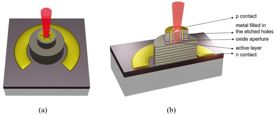
Figure 1. (a) Schematic of MuHA VCSELs. (b) Schematic cross-section of MuHA VCSELs.
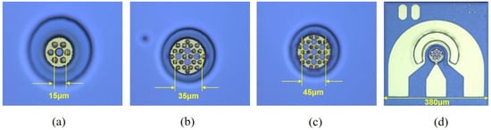
Figure 2. The microscope picture of the top mesa with (a) one aperture, (b) four apertures, and (c) seven apertures. (d) The microscope picture of the MAV with seven apertures. A number of holes are arranged in a symmetric hexagonal.
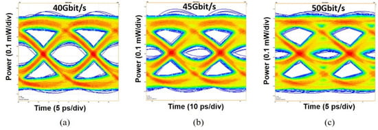
Figure 3. The eye diagram of hexagon-shape MAVs with seven 2.0-μm apertures across a 100 m-length MMF, (a) 40 Gbit/s, (b) 45 Gbit/s, (c) 50 Gbit/s.
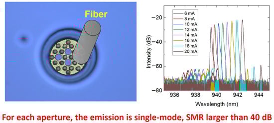
Figure 4. Optical spectrum of one of the apertures of a four aperture MAV based on a hexagonal arrangement of holes.
References
- Global Internet Growth and Trends (Source: Cisco VNI Global IP Traffic Forecast, 2017–2022). Available online: https://www.cisco.com/c/en/us/solutions/collateral/executive-perspectives/annual-internet-report/white-paper-c11-741490.pdf (accessed on 9 March 2020).
- Tian, S.-C.; Ahamed, M.; Larisch, G.; Bimberg, D. Novel energy-efficient designs of vertical-cavity surface emitting lasers for the next generations of photonic systems. Jpn. J. Appl. Phys. 2022, 61, SK0801.
- Iga, K. Surface-emitting laser-its birth and generation of new optoelectronics field. IEEE J. Sel. Top. Quantum Electron. 2000, 6, 1201–1215.
- Tatum, J.A.; Gazula, D.; Graham, L.A.; Guenter, J.K.; Johnson, R.H.; King, J.; Kocot, C.; Landry, G.D.; Lyubomirsky, I.; MacInnes, A.N.; et al. VCSEL-Based Interconnects for Current and Future Data Centers. J. Light. Technol. 2015, 33, 727–732.
- Mahgerefteh, D.; Thompson, C.; Cole, C.; Denoyer, G.; Nguyen, T.; Lyubomirsky, I.; Kocot, C.; Tatum, J. Techno-Economic Comparison of Silicon Photonics and Multimode VCSELs. J. Light. Technol. 2016, 34, 233–242.
- Moser, P.; Lott, J.A.; Larisch, G.; Bimberg, D. Impact of the Oxide-Aperture Diameter on the Energy Efficiency, Bandwidth, and Temperature Stability of 980-nm VCSELs. J. Light. Technol. 2015, 33, 825–831.
- Eiselt, N.; Griesser, H.; Wei, J.; Hohenleitner, R.; Dochhan, A.; Ortsiefer, M.; Eiselt, M.H.; Neumeyr, C.; Olmos, J.J.V.; Monroy, I.T. Experimental Demonstration of 84 Gb/s PAM-4 Over up to 1.6 km SSMF Using a 20-GHz VCSEL at 1525 nm. J. Light. Technol. 2017, 35, 1342–1349.
- Kuchta, D.M.; Rylyakov, A.V.; Doany, F.E.; Schow, C.L.; Proesel, J.E.; Baks, C.W.; Westbergh, P.; Gustavsson, J.S.; Larsson, A. A 71-Gb/s NRZ Modulated 850-nm VCSEL-Based Optical Link. IEEE Photonics Technol. Lett. 2015, 27, 577–580.
- Szczerba, K.; Westbergh, P.; Karlsson, M.; Andrekson, P.A.; Larsson, A. 70 Gbps 4-PAM and 56 Gbps 8-PAM Using an 850 nm VCSEL. J. Light. Technol. 2015, 33, 1395–1401.
- Larisch, G.; Rosales, R.; Bimberg, D. Energy-Efficient 50+ Gb/s VCSELs for 200+ Gb/s Optical Interconnects. IEEE J. Sel. Top. Quantum Electron. 2019, 25, 1701105.
- Moser, P.; Lott, J.A.; Wolf, P.; Larisch, G.; Li, H.; Ledentsov, N.N.; Bimberg, D. 56 fJ dissipated energy per bit of oxide-confined 850 nm VCSELs operating at 25 Gbit/s. Electron. Lett. 2012, 48, 1292–1294.
- Bimberg, D. Novel VCSEL Designs for the next generation of photonic systems. In Proceedings of the 2021 26th Microoptics Conference (MOC), Shizuoka, Japan, 26–29 September 2021; pp. 1–2.
- Haglund, E.; Westbergh, P.; Gustavsson, J.S.; Haglund, E.P.; Larsson, A.; Geen, M.; Joel, A. 30 GHz bandwidth 850 nm VCSEL with sub-100 fJ/bit energy dissipation at 25–50 Gbit/s. Electron. Lett. 2015, 51, 1096–1098.
- Tatum, J.A.; Landry, G.D.; Gazula, D.; Wade, J.K.; Westbergh, P. VCSEL-Based Optical Transceivers for Future Data Center Applications. In Proceedings of the Optical Fiber Communication Conference, San Diego, CA, USA, 11 March 2018; p. M3F.6.
- Feng, M.; Wu, C.; Holonyak, N. Oxide-Confined VCSELs for High-Speed Optical Interconnects. IEEE J. Quantum Electron. 2018, 54, 2400115.
- Chorchos, L.; Ledentsov, N.; Kropp, J.R.; Shchukin, V.A.; Kalosha, V.P.; Lewandowski, A.; Turkiewicz, J.P.; Ledentsov, N.N. Energy Efficient 850 nm VCSEL Based Optical Transmitter and Receiver Link Capable of 80 Gbit/s NRZ Multi-Mode Fiber Data Transmission. J. Light. Technol. 2020, 38, 1747–1752.
- Moser, P.; Lott, J.A.; Bimberg, D. Energy Efficiency of Directly Modulated Oxide-Confined High Bit Rate 850-nm VCSELs for Optical Interconnects. IEEE J. Sel. Top. Quantum Electron. 2013, 19, 1702212.
- Moser, P.; Hofmann, W.; Wolf, P.; Lott, J.A.; Larisch, G.; Payusov, A.; Ledentsov, N.N.; Bimberg, D. 81 fJ/bit energy-to-data ratio of 850 nm vertical-cavity surface-emitting lasers for optical interconnects. Appl. Phys. Lett. 2011, 98, 231106.
- Moser, P.; Lott, J.A.; Wolf, P.; Larisch, G.; Payusov, A.; Ledentsov, N.N.; Hofmann, W.; Bimberg, D. 99 fJ/(bit ·km) Energy to Data-Distance Ratio at 17 Gb/s Across 1 km of Multimode Optical Fiber With 850-nm Single-Mode VCSELs. IEEE Photonics Technol. Lett. 2012, 24, 19–21.
- Wolf, P.; Moser, P.; Larisch, G.; Li, H.; Lott, J.A.; Bimberg, D. Energy efficient 40 Gbit/s transmission with 850 nm VCSELs at 108 fJ/bit dissipated heat. Electron. Lett. 2013, 49, 666–667.
- Matsuo, S.; Sato, T.; Takeda, K.; Shinya, A.; Nozaki, K.; Taniyama, H.; Notomi, M.; Hasebe, K.; Kakitsuka, T. Ultralow Operating Energy Electrically Driven Photonic Crystal Lasers. IEEE J. Sel. Top. Quantum Electron. 2013, 19, 4900311.
- Nasu, H. Short-Reach Optical Interconnects Employing High-Density Parallel-Optical Modules. IEEE J. Sel. Top. Quantum Electron. 2010, 16, 1337–1346.
- Larisch, G.; Moser, P.; Lott, J.A.; Bimberg, D. Impact of Photon Lifetime on the Temperature Stability of 50 Gb/s 980 nm VCSELs. IEEE Photonics Technol. Lett. 2016, 28, 2327–2330.
- Li, H.; Wolf, P.; Moser, P.; Larisch, G.; Mutig, A.; Lott, J.A.; Bimberg, D. Energy-efficient and temperature-stable oxide-confined 980 nm VCSELs operating error-free at 38 Gbit/s at 85 degrees C. Electron. Lett. 2014, 50, 103–104.
- Moser, P.; Lott, J.A.; Wolf, P.; Larisch, G.; Li, H.; Bimberg, D. Error-free 46 Gbit/s operation of oxide-confined 980 nm VCSELs at 85 °C. Electron. Lett. 2014, 50, 1369–1371.
- Simpanen, E.; Gustavsson, J.S.; Haglund, E.; Haglund, E.P.; Larsson, A.; Sorin, W.V.; Mathai, S.; Tan, M.R. 1060 nm single-mode vertical-cavity surface-emitting laser operating at 50 Gbit/s data rate. Electron. Lett. 2017, 53, 869–871.
- Imai, S.; Takaki, K.; Kamiya, S.; Shimizu, H.; Yoshida, J.; Kawakita, Y.; Takagi, T.; Hiraiwa, K.; Shimizu, H.; Suzuki, T.; et al. Recorded Low Power Dissipation in Highly Reliable 1060-nm VCSELs for “Green” Optical Interconnection. IEEE J. Sel. Top. Quantum Electron. 2011, 17, 1614–1620.
- Chang, Y.-C.; Wang, C.S.; Coldren, L.A. High-efficiency, high-speed VCSELs with 35 Gbit/s error-free operation. Electron. Lett. 2007, 43, 1022–1023.
- Hatakeyama, H.; Akagawa, T.; Fukatsu, K.; Suzuki, N.; Tokutome, K.; Yashiki, K.; Anan, T.; Tsuji, M. 25 Gbit/s 100 °C operation of highly reliable InGaAs/GaAsP-VCSELs. Electron. Lett. 2009, 45, 45–46.
- Larisch, G.; Tian, S.; Bimberg, D. Optimization of VCSEL photon lifetime for minimum energy consumption at varying bit rates. Opt. Express 2020, 28, 18931–18937.
- Larisch, G.; Tian, S.C.; Bimberg, D. "Radiation Emitter". US 17 327 328, 14 April 2021.
- Larisch, G.; Tian, S.C.; Bimberg, D. "Radiation Emitter". EP 21 168 265.3, 14 April 2020.
- Larisch, G.; Tian, S.C.; Bimberg, D. "Radiation Emitter". US 17 170 834, 8 February 2021.
- Larisch, G.; Tian, S.C.; Bimberg, D. "Radiation Emitter". EP 20 192 355.4, 24 August 2020.
- Mansoor, A.; Tian, S.C.; Lindner, J.; Larisch, G.; Bimberg, D. Multi-aperture VCSELs: High power, low resistance, single mode. In Proceedings of the 2021 27th International Semiconductor Laser Conference (ISLC), Potsdam, Germany, 10–14 October 2021; pp. 1–2.
More
Information
Subjects:
Physics, Applied
Contributors
MDPI registered users' name will be linked to their SciProfiles pages. To register with us, please refer to https://encyclopedia.pub/register
:
View Times:
1.1K
Revisions:
2 times
(View History)
Update Date:
13 Apr 2023
Table of Contents


Notice
You are not a member of the advisory board for this topic. If you want to update advisory board member profile, please contact office@encyclopedia.pub.
OK
Confirm
Only members of the Encyclopedia advisory board for this topic are allowed to note entries. Would you like to become an advisory board member of the Encyclopedia?
Yes
No
${ textCharacter }/${ maxCharacter }
Submit
Cancel
Back
Comments
${ item }
|
${ item.createdUser.fullName }
${ item.createdAt }
${ item.vote }
${ item.reply }
Delete
${ reply.createdUser.fullName }
${ reply.createdAt }
${ reply.vote }
Delete
There is no reply to this comment~
${ item.replyTextCharacter }/${ item.replyMaxCharacter }
Submit
Cancel
More
No more~
There is no comment~
${ textCharacter }/${ maxCharacter }
Submit
Cancel
${ selectedItem.replyTextCharacter }/${ selectedItem.replyMaxCharacter }
Submit
Cancel
Confirm
Are you sure to Delete?
Yes
No