Submitted Successfully!
To reward your contribution, here is a gift for you: A free trial for our video production service.
Thank you for your contribution! You can also upload a video entry or images related to this topic.
Version Summary Created by Modification Content Size Created at Operation
1 -- 2343 2022-12-15 09:51:01 |
2 update references and layout + 9 word(s) 2352 2022-12-16 02:00:27 | |
3 update layout + 3 word(s) 2355 2022-12-23 03:25:40 |

Video Upload Options

Do you have a full video?

Confirm

Are you sure to Delete?
Cite
If you have any further questions, please contact Encyclopedia Editorial Office.
Kumar, A.;  Moradpour, M.;  Losito, M.;  Franke, W.;  Ramasamy, S.;  Baccoli, R.;  Gatto, G. Wide Band Gap Devices. Encyclopedia. Available online: https://encyclopedia.pub/entry/38808 (accessed on 29 April 2024).
Kumar A,  Moradpour M,  Losito M,  Franke W,  Ramasamy S,  Baccoli R, et al. Wide Band Gap Devices. Encyclopedia. Available at: https://encyclopedia.pub/entry/38808. Accessed April 29, 2024.
Kumar, Amit, Milad Moradpour, Michele Losito, Wulf-Toke Franke, Suganthi Ramasamy, Roberto Baccoli, Gianluca Gatto. "Wide Band Gap Devices" Encyclopedia, https://encyclopedia.pub/entry/38808 (accessed April 29, 2024).
Kumar, A.,  Moradpour, M.,  Losito, M.,  Franke, W.,  Ramasamy, S.,  Baccoli, R., & Gatto, G. (2022, December 15). Wide Band Gap Devices. In Encyclopedia. https://encyclopedia.pub/entry/38808
Kumar, Amit, et al. "Wide Band Gap Devices." Encyclopedia. Web. 15 December, 2022.
Wide Band Gap Devices
Edit

A decisive property that regulates semiconductor’s electrical and optical properties is the band gap, which is an important physical parameter for designating a wide band gap (WBG) semiconductor, and is defined as the energy needed for electrons to transition to the conduction band from the valence band. The magnetic property of the semiconducting materials also plays an important role for choosing of power devices in terms of energy efficiency with hysteresis and eddy current losses. The WBG semiconductor materials exhibit larger band gaps (2–4 eV) than their silicon (1–1.5 eV) counterparts and offer greater power efficiency, lower overall cost, smaller size, lighter weight, and lower energy consumption. WBG-based components in semiconductor devices permit its operation at high temperatures, which can be problematic when using conventional silicon semiconductors with smaller band gaps. The wider the bandgap, the higher the temperature at which the semiconductor power devices can function.

wide bandgap silicon carbide gallium nitride power electronics

1. Why Wide Band Gap (WBG) Semiconductor Power Devices?

By the virtue of several decades of improvement in fabrication and optimisation, a great amount of material supply, an immense manufacturing facility, and an exceptionally low cost, Si remains the most exploited element for production of power semiconductor devices due to the technology availability and materials accessibility [1]. Where there is a requirement for high power density, or high-voltage devices working at high frequencies and temperatures greater than 150 °C, Si-based devices are not able to meet the demand for advanced power electronics [2]. According to the current scenario, WBG-based power devices are used mostly because of their performances and efficiency [3]. In recent years several semiconductor devices, along with Gallium nitride (GaN) and  silicon carbide (SiC)  power devices have been advanced and investigated. At present, SiC and GaN are seen as more promising semiconductors materials because of their efficiency, the market availability of basic materials, and the maturity of their technologies. Thus, WBG materials such as SiC and GaN have attracted huge attention as they represent a good alternative to silicon owing to their superior physical and electrical properties. Overall, amongst WBC semiconductor materials, SiC and GaN are the leading ones and are also attractive for high-power electronics, from the device maker perspective [4]. It is valuable to note that WBG power devices show better productivity for power applications and likewise have a capacity of high-temperature resilience [5]. WBG power semiconductor devices show an ordinary expansion in impeding the voltage and transmission current appraisals and works likewise on higher frequencies, power levels, and higher voltages. In the power conversion industry, GaN-based power devices play a key role within smart phones, computers, battery chargers, automotive, lighting systems and photovoltaics [6][7].
In power electronics systems, the usage of WBG power devices can lead to optimized design solutions in terms of passive components, converter topologies, and thermal management. WBG-based power devices play an important role in different applications [8], and because of their properties, these materials have become suitable for reducing the volume, weight, and costs. In order to accommodate the high power and frequencies, several manufacturers are using WBG materials for electric vehicles, and other applications since it outperforms the limits of silicon and guarantees excellent performance in critical operating environments. SiC and GaN are ideal representatives of the WBG semiconductor materials, and are widely used as technology materials to make things simpler, faster, and smaller and have great efficiency in performance.
The first WBG power devices that reached the highest technology readiness levels [9] are n-type SiC power metal oxide semiconductor field effect transistors (MOSFET), SiC-based Schottky-barrier diodes and GaN high electron mobility transistors (HEMT). With the aim to target power electronics applications, these devices have been in high volume production for a few years. For commercial applications, the main advantage of SiC is seen in the applications requiring voltages above 650 V such as electrical vehicle chargers and solar power inverters. At the same time, GaN devices are a preferable choice for replacing Si devices in applications at voltages below 650 V. With the maturing of these new semiconductor technologies, the market for SiC and GaN will only grow further. Significant improvements in future renewable energy distribution can be supported from fabrication of SiC Insulated Gate Bipolar Transistor (IGBT) and super junction (SJ) MOSFET. On the other hand, the potential of GaN power devices can be mainly foreseen for high frequency power electronics [1].

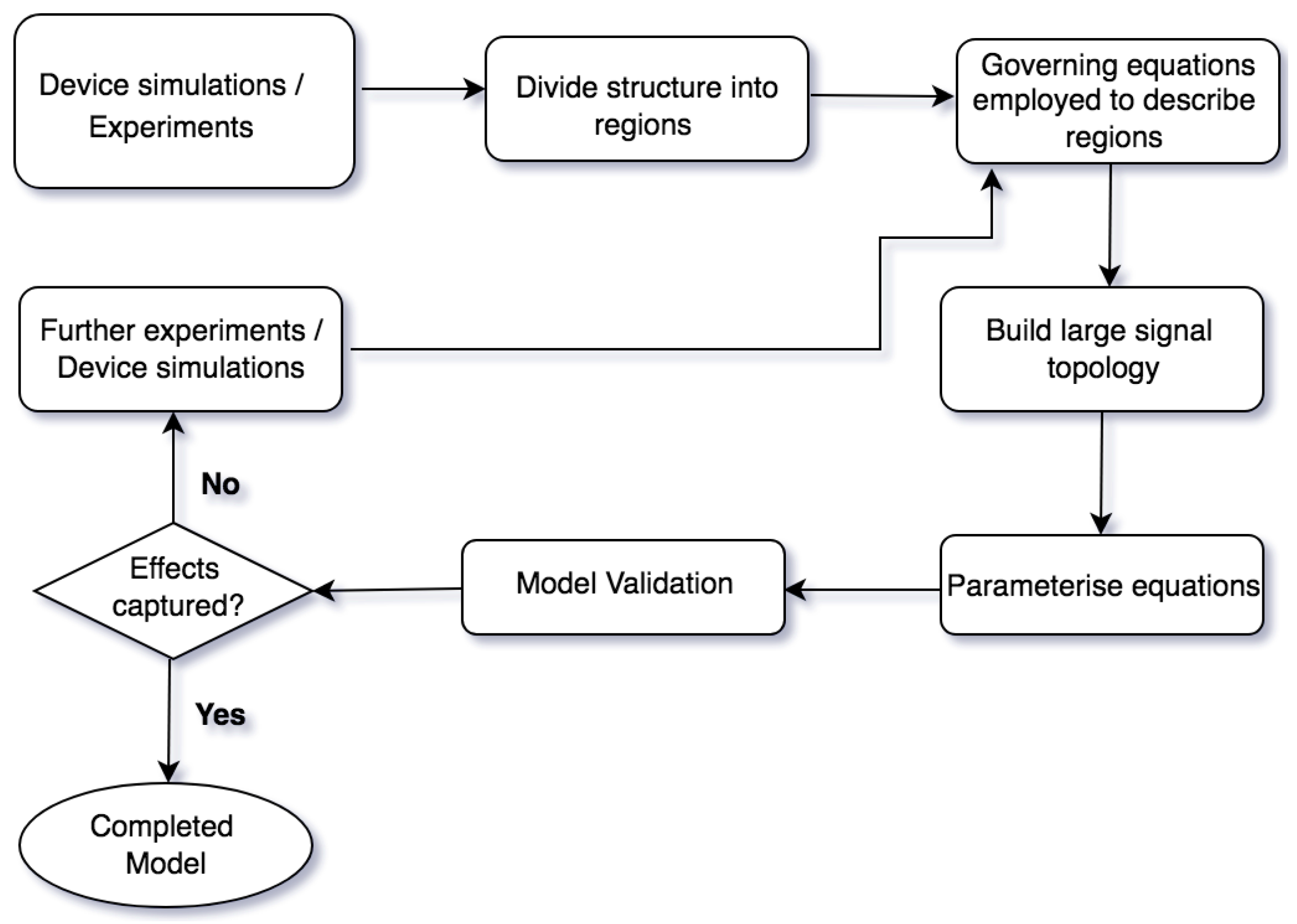
2. Models of Semiconductor Power Devices

Modeling of power semiconductor devices is essential to estimate their impact on cost, efficiency, weight, volume, and reliability, which are important performance indices of power electronic systems. These indices are mutually coupled to each other; for instance, high power densities imply high switching frequencies, which can lead to a reduction in efficiency. Prior to the fabrication of new device structures, they can be accurately investigated by modelling. It is essential to consider several physical effects with high priority for the development of power semiconductor device models, since they dominate the static and dynamic device characteristics [10][11]. In particular, the models for new devices must be able to mimic the device behavior in both static and dynamic conditions. However, if a new device shares certain related characteristics with a prevalent device, then it can be modelled by adjusting the approach of the known device [12].
A compact device modelling approach aims to predict details of the current flow across the device as a function of the applied currents and voltages, physical characteristics (geometry, doping levels), and environmental conditions (temperature and radiation) [13]. These models are based on an equivalent electrical circuit consisting of lumped circuit elements (resistors, inductors, capacitors and controlled current or voltage sources). The approach includes relations of current–voltage (I–V) and charge/capacitance–voltage (Q/C-V) for nonlinear lumped elements defined by closed-form expressions with parameter values that are based on underlying physics or extracted from experimental measurements [14]. It is paramount to achieve a good estimate to the existing association of the electrical variables. Moreover, to achieve fast simulation time, a compromise between computational speed and model accuracy is usually involved that can affect the prediction of dynamic performance of the device. Thus, the simulation time and accuracy become pivotal factors to be examined by device model engineers when considering this accord [13].
In the literature, modeling of power semiconductor devices has been reported to be performed using behavioral, semi-physics, physics-based, semi-numerical, and numerical/analytical models [13]. Behavioral models are used to represent the device behavior rather than the device physics based on functions, and are considered a good trade-off between accuracy and simulation time [15]. Using mathematical techniques and correspondent circuits, a relatively high simulation speed can be achieved by behavioral models, but physics-based understanding into the device behavior is lost [16][17]. Semi-physics models are somewhat based on device physics, wherein standard low voltage device models available from circuit simulation tools (SABER, SPICE) are remodeled to focus on the high-voltage power device design. As a consequence, the physical meaning of a few device model parameters can be lost. On the other hand, physics-based modeling tools are more accurate, but time-consuming and require many fabrication parameters.
The outline of the physics-based model approach is shown in Figure 1. In the first phase, device characterization is performed by experiments and numerical simulations on the model device structure. By analyzing the results, model equations are formulated using physics assumptions of depleted regions, field effects, charge transport, etc. The equations are parameterized using measured data as a basis and a large signal topology is built. The model is then validated by implementing for the target simulator and comparing the measured data with the simulated one. The model is considered completed only if it is able to capture the necessary effects; if not, the model should be improved and the process is repeated again [13].
Figure 1. Physics-based model approach.
Semi-numerical models can be seen as in-between physics and numerical models. In this approach, external electrical characteristics, internal physical and electrical information, carrier distribution and junction temperature in various regions of the device can be realized by applying numerical algorithms such as Laplace transformation, Fourier series, difference methods, and internal approximation to solve the ambipolar diffusion equation (ADE). Due to high level injection, the ADE is assumed to be one-dimensional, which is valid for the power semiconductor devices [18]. The numerical models provide very accurate results and can significantly contribute to the development of power devices, but are computationally intensive, complicated, and require exhaustive information on device geometry and material properties. Popular numerical simulation tools available for power devices and circuit simulation are TCAD [19][20], MEDICI [21], SILVACO [22], Sentaurus [23] and so on.
Analytical models, on the other hand, are relatively quick for data processing, but have issues with improvement in accuracy. This approach is dedicated primarily for a quick evaluation of switching losses, and is based on datasheet information [17] such as input capacitances, transconductance, switching delay times and rise/fall switching times [24], or empirical formulas derived from measurements [25][26]. Langmaack et al. [27] presented a low calculation time effort approach that incorporated the use of analytical description of loss terms with numerical circuit simulations. This method has been successfully adopted for comparison of different modulation schemes and device technologies of semiconductor devices such as Si IGBT, SiC MOSFET and GaN HEMT. However, developing analytical models for switching power losses that are valid for a wide range of operating points based on datasheets or measurements is not feasible, since these losses highly depend on the parasitics associated with the circuit and package layouts.

3. Merits and Challenges of Using WBG Semiconductor Devices

Along with the silicon-based semiconductor, WBG semiconductors have the capability for compact, robust, and efficient power conversion systems [28]. WBG semiconductor materials in electrical power switching devices enable a transformative influence on a wide range of energy conversion applications. WBG semiconductor-based devices are thinner and display lower on-resistances, which implies lower conduction losses and an overall superior converter efficiency. From a technological point of view, SiC is the most advanced form among the current WBG power device materials. SiC has a clear advantage on higher blocking voltage, better switching speeds, and low conduction loss compared to Si [29]. WBG semiconductors are also thermally stable and their use in power switching devices permit to reduce volume, weight, and life cycle costs [30].
WBG provides many advantages like handling higher voltages and power, faster switching, better efficiency, and higher operating temperatures [31]. Power devices with semiconductor material SiC have less effect on functionality, and continue to work even when the temperature rises up to 600 °C [32]. WBG semiconductor-based power devices are more reliable as with temperature and time only slight fluctuation is noted in its forward and reverse characteristics. WBG power devices are smaller, faster, and more reliable and operate on higher frequencies, power levels, and higher voltages [33]. WBG semiconductor devices have better efficiency and enable high-power density converters, exhibit superior power operating speeds, and an improved efficiency for power conversions [28][34][35].
For high-power applications, SiC MOSFETs display superior switching speed, and thus operate at higher switching frequencies than Si IGBTs [36]. GaN-based HEMTs function at switching frequencies higher than that of Si MOSFETs, considering low-power applications [37][38][39]. The extremely fast switching and the material properties of WBG devices have posed new challenges to their applications. The major challenges include switching frequencies in the hundreds of kHz to MHz range, rapid current and voltage slopes triggering the effects of capacitive couplings and parasitic inductive, and unusual electromagnetic interference (EMI) emission. By virtue of high switching frequency, WBG power devices are more susceptible to EMI, a phenomenon that occurs when an electronic device is exposed to an electromagnetic (EM) field [40][41]. Despite the fact that for applications requiring high-power, the switching frequencies are not as high compared to applications requiring low-power, EMI still remains notable since the amplitude of switching voltages and currents are high. On the contrary, for low-power applications, the magnitude of switching currents and voltages can be smaller than those in high-power, however, since the devices operate at a high frequency EMI’s presence is significant [42]. EMI propagation paths and EMI noise source characteristics are key to compare the EMI performance of Si devices and WBG devices. Tretin et al. [43] compared conductive EMI between matrix converters with Si IGBTs (switching speed 6.6 kV/μs) and SiC MOSFETs (11 kV/μs) at 10 KHz switching frequency. The EMI noise of SiC MOSFET was found to be 20 dB higher compared to Si IGBT from 10–30 MHz [43]. For a 1kW 400 V GaN HEMT device, the conducted EMI measured was found to be 20 dB higher at 500 KHz switching frequency compared to EMI at 50 kHz switching frequency. Thus, the conductive EMI is the most severe when WBG devices function at higher switching frequency and speed compared to Si-devices [44].
To reduce the noise-levels generated by the power converters, most devices contain an EMI passive filter whose use remains a challenge towards enabling high power density [45]. EMI shielding is a process that involves preventing the penetration of the harmful EM radiations into the electronic devices [46]. It is one of the best methods to protect the health of living beings as well as the environment from the negative impacts of EM waves [47]. The passive filter occupies nearly 30% of the power electronics converter system’s volume and its use is inevitable to guarantee compliance with conducted EMI standards. To reduce the submissive EMI filter volume is a big task for the power generator designers [48]. Active EMI filters (AEF) in this context display great promise in minimizing the volume of the passive component (with reductions higher than 50%) in power converters [49][50][51]. In [52], the authors provided an overview of several works in the area of AEFs and their implementations for different power converters in the past three decades. The topology of AEFs [53] are built on rating of sensing and cancellation components and kind of source and load impedances. Other techniques such as using small propagation paths and by using small passive components have also been suggested to reduce the system’s volume [54]. However, the most common EMI problems are power disturbances because of different filters [55], due to which units, circuits, and wires can never contain complete electricity, and EMI shielding currently has a bigger concern. Moreover, an EMI filter’s performance at high frequency is restricted by the filter’s parasitic parameters and the magnetic material, thus making it challenging to reduce high frequency EMI noise [56].

References

  1. Gachovska, T.K.; Hudgins, J.L. SiC and GaN Power Semiconductor Devices. In Power Electronics Handbook; Butterworth-Heinemann: Woburn, MA, USA, 2018; pp. 95–155.
  2. Raynaud, C.; Tournier, D.; Morel, H.; Planson, D. Comparison of high voltage and high temperature performances of wide bandgap semiconductors for vertical power devices. Diamond Relat. Mater. 2010, 19, 1–6.
  3. Roccaforte, F.; Fiorenza, P.; Greco, G.; Lo Nigro, R.; Giannazzo, F.; Iucolano, F.; Saggio, M. Emerging trends in wide band gap semiconductors (SiC and GaN) technology for power devices. Microelectron. Eng. 2018, 187–188, 66–77.
  4. Pu, T.; Younis, U.; Chiu, H.-C.; Xu, K.; Kuo, H.-C.; Liu, X. Review of Recent Progress on Vertical GaN-Based PN Diodes. Nanoscale Res. Lett. 2021, 16, 101.
  5. Shah, F.M.; Xiao, H.M.; Li, R.; Awais, M.; Zhou, G.; Bitew, G.T. Comparative performance evaluation of temperature dependent characteristics and power converter using GaN, SiC and Si power devices. In Proceedings of the 2018 IEEE 12th International Conference on Compatibility, Power Electronics and Power Engineering (CPE-POWERENG 2018), Doha, Qatar, 10–12 April 2018; pp. 1–7.
  6. Amano, H.; Baines, Y.; Beam, E.; Borga, M.; Bouchet, T.; Chalker, P.R.; Charles, M.; Chen, K.J.; Chowdhury, N.; Chu, R.; et al. The 2018 GaN power electronics roadmap. J. Phys. D Appl. Phys. 2018, 51, 163001.
  7. Kaminski, N.; Hilt, O. SiC and GaN devices—Wide bandgap is not all the same. IET Circuits Devices Syst. 2014, 8, 227–236.
  8. Chang, G.A.; Jin, H.; Qin, L.; Zhang, L.; Zeng, X.; Yang, R.; Ma, M.; Arumuga Perumal, S.; Chen, G. Review of wide band-gap semiconductors technology. MATEC Web Conf. 2016, 40, 1006.
  9. Brueniger, R.D.; Andersen, A.; Wulff, J.; Makoschitz, M.; Krischan, K.; Bergmann, P. Wide Band Gap Technology: Efficiency Potential and Application Readiness Map 4E Power Electronic Conversion Technology Annex (PECTA). Available online: https://www.iea-4e.org/wp-content/uploads/publications/2020/05/PECTA_Report_Total-V10final-May-2020.pdf (accessed on 8 August 2022).
  10. Santi, E.; Peng, K.; Mantooth, H.A.; Hudgins, J.L. Modeling of Wide-Bandgap Power Semiconductor Devices—Part II. IEEE Trans. Electron Devices 2015, 62, 434–442.
  11. Kraus, R.; Mattausch, H.J. Status and trends of power semiconductor device models for circuit simulation. IEEE Trans. Power Electron. 1998, 13, 452–465.
  12. Bottaro, E.; Rizzo, S.A.; Salerno, N. Circuit Models of Power MOSFETs Leading the Way of GaN HEMT Modelling—A Review. Energies 2022, 15, 3415.
  13. Mantooth, H.A.; Peng, K.; Santi, E.; Hudgins, J.L. Modeling of Wide Bandgap Power Semiconductor Devices—Part I. IEEE Trans. Electron Devices 2015, 62, 423–433.
  14. Root, D. Future Device Modeling Trends. IEEE Microw. Mag. 2012, 13, 45–59.
  15. Paula, W.J.; Tavares, G.H.M.; Soares, G.M.; Almeida, P.S.; Braga, H.A.C. Switching losses prediction methods oriented to power MOSFETs—A review. IET Power Electron. 2020, 13, 2960–2970.
  16. Ahmed, M.R.; Todd, R.; Forsyth, A.J. Predicting SiC MOSFET Behavior Under Hard-Switching, Soft-Switching, and False Turn-On Conditions. IEEE Trans. Ind. Electron. 2017, 64, 9001–9011.
  17. Xu, Y.; Ho, C.N.M.; Ghosh, A.; Muthumuni, D. A Datasheet-Based Behavioral Model of SiC MOSFET for Power Loss Prediction in Electromagnetic Transient Simulation. In Proceedings of the 2019 IEEE Applied Power Electronics Conference and Exposition (APEC), Anaheim, CA, USA, 17–21 March 2019; pp. 521–526.
  18. Santi, E.; Hudgins, J.L.; Mantooth, H.A. Variable Model Levels for Power Semiconductor Devices. In Proceedings of the SCSC07:2007 Summer Computer Simulation Conference, San Diego, CA, USA, 16–19 July 2007; pp. 276–283.
  19. Jun-Ha, L.; Hoong-Joo, L. Circuit model parameter generation with TCAD simulation. In Proceedings of the 7th International Conference on Solid-State and Integrated Circuits Technology, Beijing, China, 18–21 October 2004; pp. 1084–1087.
  20. Campian, I.; Profirescu, O.G.; Ungureanu, A.; Babarada, F.; Lakatos, E.; Amza, C. MOSFET simulation-TCAD tools/packages. In Proceedings of the 2003 International Semiconductor Conference, CAS 2003 Proceedings (IEEE Cat. No.03TH8676), Sinaia, Romania, 28 September–2 October 2003; pp. 235–238.
  21. Liou, J.J.; Ortiz-Conde, A.; Garcia-Sanchez, F. MOSFET simulation using device Simulators. In Analysis and Design of Mosfets; Springer: Boston, MA, USA, 1998; pp. 109–162.
  22. Ammi, S.; Aissat, A.; Wichmann, N.; Bollaert, S. III-V MOSFET Structure (InP/InAs/InGaAs) I-V Characteristics Using Silvaco TCAD Simulator. In Proceedings of the 1st International Conference on Electronic Engineering and Renewable Energy, Saidia, Morocco, 15–17 April 2018; pp. 207–215.
  23. Lophitis, N.; Arvanitopoulos, A.; Perkins, S.; Antoniou, M. TCAD Device Modelling and Simulation of Wide Bandgap Power Semiconductors. In Disruptive Wide Bandgap Semiconductors, Related Technologies, and Their Applications; IntechOpen: Rijeka, Croatia, 2018.
  24. Christen, D.; Biela, J. Analytical Switching Loss Modeling Based on Datasheet Parameters for MOSFETS in a Half-Bridge. IEEE Trans. Power Electron. 2019, 34, 3700–3710.
  25. Moradpour, M.; Lai, A.; Serpi, A.; Gatto, G. Multi-objective optimization of gate driver circuit for GaN HEMT in electric vehicles. In Proceedings of the IECON 2017—43rd Annual Conference of the IEEE Industrial Electronics Society, Beijing, China, 29 October–1 November 2017; pp. 1319–1324.
  26. Burkart, R.M.; Kolar, J.W. Comparative η– ρ– σ Pareto Optimization of Si and SiC Multilevel Dual-Active-Bridge Topologies with Wide Input Voltage Range. IEEE Trans. Power Electron. 2017, 32, 5258–5270.
  27. Langmaack, N.; Schobre, T.; Henke, M. Fast and Universal Semiconductor Loss Calculation Method. In Proceedings of the 2019 IEEE 13th International Conference on Power Electronics and Drive Systems (PEDS), Toulouse, France, 9–12 July 2019; pp. 1–4.
  28. Shenai, K. Future Prospects of Widebandgap (WBG) Semiconductor Power Switching Devices. IEEE Trans. Electron Devices 2015, 62, 248–257.
  29. Zhang, L.; Yuan, X.; Wu, X.; Shi, C.; Zhang, J.; Zhang, Y. Performance Evaluation of High-Power SiC MOSFET Modules in Comparison to Si IGBT Modules. IEEE Trans. Power Electron. 2019, 34, 1181–1196.
  30. Nguyen, N.-K.; Nguyen, T.; Nguyen, T.-K.; Yadav, S.; Dinh, T.; Masud, M.K.; Singha, P.; Do, T.N.; Barton, M.J.; Ta, H.T.; et al. Wide-Band-Gap Semiconductors for Biointegrated Electronics: Recent Advances and Future Directions. ACS Appl. Electron. Mater. 2021, 3, 1959–1981.
  31. Cha, K.-H.; Ju, C.-T.; Kim, R.-Y. Analysis and Evaluation of WBG Power Device in High Frequency Induction Heating Application. Energies 2020, 13, 5351.
  32. Li, Y.; Liang, T.; Lei, C.; Li, Q.; Li, Z.; Ghaffar, A.; Xiong, J. Study on the Stability of the Electrical Connection of High-Temperature Pressure Sensor Based on the Piezoresistive Effect of P-Type SiC. Micromachines 2021, 12, 216.
  33. Sullivan, C.R.; Yao, D.; Gamache, G.; Latham, A.; Qiu, J. (Invited) Passive Component Technologies for Advanced Power Conversion Enabled by Wide-Band-Gap Power Devices. ECS Trans. 2019, 41, 315–330.
  34. Shenai, K. Wide bandgap (WBG) semiconductor power converters for DC microgrid applications. In Proceedings of the 2015 IEEE First International Conference on DC Microgrids (ICDCM), Atlanta, GA, USA, 7–10 June 2015; pp. 263–268.
  35. Huang, A.Q. Wide bandgap (WBG) power devices and their impacts on power delivery systems. In Proceedings of the 2016 IEEE International Electron Devices Meeting (IEDM), San Francisco, CA, USA, 3–7 December 2016; pp. 20.21.21–20.21.24.
  36. Fuentes, C.D.; Müller, M.; Bernet, S.; Kouro, S. SiC-MOSFET or Si-IGBT: Comparison of Design and Key Characteristics of a 690 V Grid-Tied Industrial Two-Level Voltage Source Converter. Energies 2021, 14, 3054.
  37. Wang, B.; Dong, S.; Jiang, S.; He, C.; Hu, J.; Ye, H.; Ding, X. A Comparative Study on the Switching Performance of GaN and Si Power Devices for Bipolar Complementary Modulated Converter Legs. Energies 2019, 12, 1146.
  38. Zhang, Y.; Wang, S.; Chu, Y. Comparison of Radiated Electromagnetic Interference (EMI) Generated by Power Converters with Silicon MOSFETs and GaN HEMTs. In Proceedings of the 2019 IEEE Applied Power Electronics Conference and Exposition (APEC), Anaheim, CA, USA, 17–21 March 2019; pp. 1375–1382.
  39. Han, D.; Morris, C.T.; Lee, W.; Sarlioglu, B. A Case Study on Common Mode Electromagnetic Interference Characteristics of GaN HEMT and Si MOSFET Power Converters for EV/HEVs. IEEE Trans. Transp. Electrif. 2017, 3, 168–179.
  40. Pirino, P.; Losito, M.; Kumar, A.; Gatto, G.; Meo, S.; Frank, W.-T.; Moradpour, M. Multi-Objective Gate Driver Design for a GaN-Based Half-Bridge Converter to Optimize Efficiency and Near-Field EMI. Int. Rev. Electr. Eng. (IREE) 2021, 16, 95.
  41. Mathur, P.; Raman, S. Electromagnetic Interference (EMI): Measurement and Reduction Techniques. J. Electron. Mater. 2020, 49, 2975–2998.
  42. Mortazavizadeh, S.A.; Palazzo, S.; Amendola, A.; De Santis, E.; Di Ruzza, D.; Panariello, G.; Sanseverino, A.; Velardi, F.; Busatto, G. High Frequency, High Efficiency, and High Power Density GaN-Based LLC Resonant Converter: State-of-the-Art and Perspectives. Appl. Sci. 2021, 11, 11350.
  43. Trentin, A.; de Lillo, L.; Empringham, L.; Wheeler, P.; Clare, J. Experimental Comparison of a Direct Matrix Converter Using Si IGBT and SiC MOSFETs. IEEE J. Emerg. Sel. Top. Power Electron. 2015, 3, 542–554.
  44. Middelstaedt, L.; Lindemann, A. Methodology for analysing radiated EMI characteristics using transient time domain measurements. IET Power Electron. 2016, 9, 2013–2018.
  45. Schittler, A.C.; Pappis, D.; Zacharias, P. EMI filter design for high switching speed and frequency grid-connected inverters. In Proceedings of the 2016 18th European Conference on Power Electronics and Applications (EPE’16 ECCE Europe), Karlsruhe, Germany, 5–9 September 2016; pp. 1–8.
  46. Ouyang, X.; Huang, W.; Cabrera, E.; Castro, J.; Lee, L.J. Graphene-graphene oxide-graphene hybrid nanopapers with superior mechanical, gas barrier and electrical properties. AIP Adv. 2015, 5, 017135.
  47. Sankaran, S.; Deshmukh, K.; Ahamed, M.B.; Khadheer Pasha, S.K. Recent advances in electromagnetic interference shielding properties of metal and carbon filler reinforced flexible polymer composites: A review. Compos. Part A Appl. Sci. Manuf. 2018, 114, 49–71.
  48. Akagi, H.; Hasegawa, H.; Doumoto, T. Design and Performance of a Passive EMI Filter for Use With a Voltage-Source PWM Inverter Having Sinusoidal Output Voltage and Zero Common-Mode Voltage. IEEE Trans. Power Electron. 2004, 19, 1069–1076.
  49. Lee, K.-H.; Kang, B.-G.; Choi, Y.; Chung, S.-K.; Won, J.-S.; Kim, H.-S. Design and Implementation of an Active EMI Filter for Common-Mode Noise Reduction. J. Power Electron. 2016, 16, 1236–1243.
  50. Biela, J.; Wirthmueller, A.; Waespe, R.; Heldwein, M.L.; Raggl, K.; Kolar, J.W. Passive and Active Hybrid Integrated EMI Filters. IEEE Trans. Power Electron. 2009, 24, 1340–1349.
  51. Ali, M.; Laboure, E.; Costa, F. Integrated Active Filter for Differential-Mode Noise Suppression. IEEE Trans. Power Electron. 2014, 29, 1053–1057.
  52. Narayanasamy, B.; Luo, F. A Survey of Active EMI Filters for Conducted EMI Noise Reduction in Power Electronic Converters. IEEE Trans. Electromagn. Compat. 2019, 61, 2040–2049.
  53. Zhou, Y.; Wang, H.; Chen, W.; Yan, R.; Liu, J.; Zhang, R. The effectiveness comparison of AEF with different sensing method in High Power Converters. In Proceedings of the 2020 IEEE 9th International Power Electronics and Motion Control Conference (IPEMC2020-ECCE Asia), Nanjing, China, 29 November–2 December 2020; pp. 1649–1652.
  54. Luo, F.; Dong, D.; Boroyevich, D.; Mattavelli, P.; Wang, S. Improving High-Frequency Performance of an Input Common Mode EMI Filter Using an Impedance-Mismatching Filter. IEEE Trans. Power Electron. 2014, 29, 5111–5115.
  55. Bernacki, K.; Wybrańczyk, D.; Zygmanowski, M.; Latko, A.; Michalak, J.; Rymarski, Z. Disturbance and Signal Filter for Power Line Communication. Electronics 2019, 8, 378.
  56. Wang, S. EMI Modeling and Reduction in Modern Power Electronics Systems. In Proceedings of the 2018 IEEE Symposium on Electromagnetic Compatibility, Signal Integrity and Power Integrity (EMC, SI & PI), Long Beach, CA, USA, July 30–August 3 2018; pp. 1–44.
More
Information
Contributors MDPI registered users' name will be linked to their SciProfiles pages. To register with us, please refer to https://encyclopedia.pub/register : , , , , , ,
View Times: 768
Revisions: 3 times (View History)
Update Date: 23 Dec 2022
1000/1000