Submitted Successfully!
To reward your contribution, here is a gift for you: A free trial for our video production service.
Thank you for your contribution! You can also upload a video entry or images related to this topic.
Version Summary Created by Modification Content Size Created at Operation
1 -- 1266 2022-08-05 20:00:00 |
2 format Meta information modification 1266 2022-08-08 04:19:45 |

Video Upload Options

Do you have a full video?

Confirm

Are you sure to Delete?
Cite
If you have any further questions, please contact Encyclopedia Editorial Office.
Ramadan, R.;  Martín-Palma, R.J. Impact of Nanostructured Silicon on Thermoelectric Performance. Encyclopedia. Available online: https://encyclopedia.pub/entry/25909 (accessed on 25 April 2024).
Ramadan R,  Martín-Palma RJ. Impact of Nanostructured Silicon on Thermoelectric Performance. Encyclopedia. Available at: https://encyclopedia.pub/entry/25909. Accessed April 25, 2024.
Ramadan, Rehab, Raúl J. Martín-Palma. "Impact of Nanostructured Silicon on Thermoelectric Performance" Encyclopedia, https://encyclopedia.pub/entry/25909 (accessed April 25, 2024).
Ramadan, R., & Martín-Palma, R.J. (2022, August 05). Impact of Nanostructured Silicon on Thermoelectric Performance. In Encyclopedia. https://encyclopedia.pub/entry/25909
Ramadan, Rehab and Raúl J. Martín-Palma. "Impact of Nanostructured Silicon on Thermoelectric Performance." Encyclopedia. Web. 05 August, 2022.
Impact of Nanostructured Silicon on Thermoelectric Performance
Edit

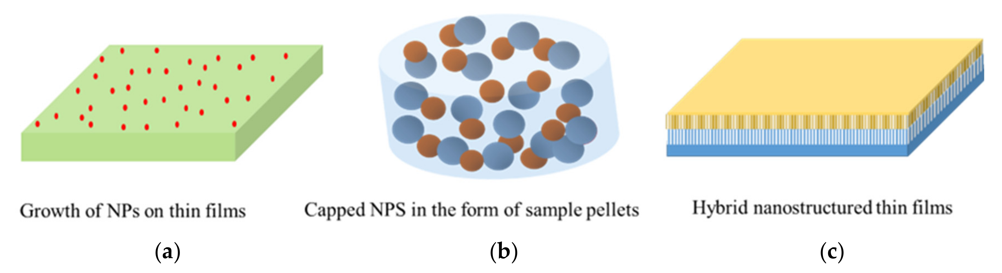
Nanostructured materials remarkably improve the overall properties of thermoelectric devices, mainly due to the increase in the surface-to-volume ratio. This behavior is attributed to an increased number of scattered phonons at the interfaces and boundaries of the nanostructures. Among many other materials, nanostructured Si was used to expand the power generation compared to bulk crystalline Si, which leads to a reduction in thermal conductivity. However, the use of nanostructured Si leads to a reduction in the electrical conductivity due to the formation of low dimensional features in the heavily doped Si regions. Accordingly, the fabrication of hybrid nanostructures based on nanostructured Si and other different nanostructured materials constitutes another strategy to combine a reduction in the thermal conductivity while keeping the good electrical conduction properties. 

thermoelectric devices phonon scattering nanostructured Si

1. Introduction

Thermoelectric devices allow power generation from waste heat. The thermoelectric effect is the direct conversion of a temperature difference to electricity or vice versa [1]. Among many other materials, bismuth telluride alloys are considered the most efficient thermoelectric materials [2]. However, these alloys are costly due to the enormous amount of expensive telluride material the alloys have, in addition to their toxicity. Crystalline Si was used to expand the power generation via the thermoelectric effect. Si is a non-toxic, inexpensive, and earth-abundant material. Various thermoelectric alloys based on Si were designed, including Si-Ge and Mg2Si alloys [3][4][5][6]. Although bulk Si has high electrical conductivity, it has a high thermal conductivity, which yields a low figure of merit (ZT) for thermoelectric devices [7].
Therefore, researchers focused on modifying methods to improve the performance of Si-based thermoelectric devices by reducing their thermal conductivity. The growth of nanostructured Si is one of the sufficient approaches to minimizing the thermal conductivity of bulk Si. Porous silicon (PSi), Si nanoparticles (SiNPs) or Si nanowires (SiNWs) are nanostructured instances suitable for enhancing the Seebeck coefficient of Si-based thermoelectric devices by reducing the thermal conductivity [8][9][10]. However, texturing the surface of Si wafers leads to a reduction in the electrical conductivity [11][12]. This behavior is attributed to the performance of the texturing in the heavily doped regions of Si substrates.

2. Si-Based Thermoelectric Materials

Non-toxicity, high industrial compatibility, low price compared with other materials, and the chemical and mechanical stability of silicon make this material a good candidate for thermoelectric applications. In addition, it shows good electrical conductivity which depends on the doping level. However, monocrystalline silicon has a high thermal conductivity of ~150 W m−1 K−1 at 300 K, which hinders the high conversion efficiency of thermoelectric devices. Thermoelectric properties of silicon were previously reported by researchers. For instance, Bux et al. measured the thermoelectric properties of bulk silicon with a Seebeck coefficient of 0.008 at 300 K [9]. This reduction in the Seebeck coefficient for silicon-based thermoelectric devices is attributed to the increase in the thermal conductivity of silicon [9][13]. Many strategies were developed to improve the thermoelectric properties of silicon material. One way is by texturing or etching the surface of the silicon substrate to increase phonon scattering in the interfaces and on the boundaries of the walls of nanostructured silicon [7][9][13]. Another perspective is by combining silicon nanostructures with another effective thermoelectric material, such as Ge and Mg [3][4][5][6][14].

3. Thermoelectric Devices Modified by Nanostructured Silicon

Nanostructured silicon can take many different forms, including porous silicon (PSi), silicon nanoparticles (SiNPs) or silicon nanowires (SiNWs). The morphology of nanostructured Si depends on the fabrication method and the fabrication parameters [15]. The increase in the surface-to-volume ratio of nanostructured Si greatly improves the thermoelectric performance due to an increased number of scattered phonons at the interfaces and boundaries of the nanowires or nanoparticles of Si. The number of surface defects is also increased. Furthermore, the reduction in the dimensions of Si nanostructures leads to increased surface roughness, resulting in a reduction in thermal conductivity.
From another perspective, nanostructured silicon in different forms has been studied as an effective thermoelectric material by many researchers in a wide range of different porosities [7][10][13]. For instance, Ting Zhang et al. presented a remarkable enhancement in the ZT values due to texturing the front and back sides of Si substrate performing Si nanowire arrays (SiNWAs). The structure of the modified device is SiNWAs/Si/SNWAs sandwich structured composites (SSC) [13]. ZT values were remarkably increased from 0.006 for bulk Si devices to 0.493 for the modified SSC at room temperature. 

4. Thermoelectric Materials Modified by Hybrid Nanocomposites

Nanostructured Si remarkably contributes to reducing the thermal conductivity of thermoelectric devices. However, etching the surface of Si substrate occurs in the heavily doped Si regions. As a result, the electrical conductivity of nanostructured Si remarkably decreases with the increase in porosity; likewise, fast oxidation of the porous silicon layer in ambient air. Accordingly, hybrid silicon nanostructures with another effective thermoelectric material dramatically reduced the thermal conductivity of nanostructured Si and maintained adequate electrical conductivity due to the other thermoelectric material, in addition to preventing nanostructured Si from oxidation due to the growth of the other thermoelectric material into the nanostructured Si layer.
Figure 1 shows a schematic representation of some of the possible hybrid nanostructures suitable for enhancing the thermoelectric properties of thermoelectric devices. Each material has a valuable effect in improving the thermoelectric properties of the implemented thermoelectric devices. For instance, Nitin Saxena et al. reported the combination of the organic PEDOT:PSS material with SiNPs. This combination leads to improving the ZT value of the fabricated thermoelectric device from 5.3 ×
10−3 without SiNPs to 8.0 × 10⁻³ at 0.5 wt% SiNPs at 300 K [14]. Furthermore, Gitanjali Kolhatkar et al. observed the stability and reduction in the thermal conductivity due to the combination of graphene and nanostructured mesoporous Si to 13 WmK1
[16]. From another perspective, the Seebeck coefficient of the atomic layer-deposited PbTe/PbSe nanolaminate structures deposited inside PSi templates significantly increased in both vertical and horizontal directions compared with the growth of the same nanolaminate on planar Si (143 μV/K), 370.556 μV/K in horizontal directions and 78,670 μV/K in vertical directions at 300 K [17].
Figure 1. Schematic representation of different hybrid nanostructures. (a) Compose of NPs/thin films, (b) Hybrid NPs in the form of pellets and (c) Hybrid nanostructured thin films for the development of efficient thermoelectric devices.
From the recorded data, the Seebeck coefficient of PbTe/PbSe (10/10 nm) nanolaminates deposited on PSi substrate is about four times higher than that of the planar sample. This enhancement is attributed to the presence of the regular arrays of nanopores. These pores lead to the increase in the surface-to-volume ratio for Si and for the grown nanolaminates, which results in a reduction in thermal conductivity. Moreover, the increase in porosity leads to an increase in the number of defects and surface roughness. So, the Seebeck coefficient increases, particularly at low temperatures.
Additionally, SiNPs show a remarkable enhancement in the thermoelectric properties compared with the bulk material. This enhancement is attributed to the increase in the number of surface defects, which leads to increasing phonon scattering between the interfaces. However, the increase in the density of SiNPs leads to a reduction in the electrical conductivity due to the formation of an oxide layer on the outer surface. 
Silicon-germanium (SiGe) alloy has been one of the thermoelectric materials most widely used for Radioisotope Thermoelectric Generators (RTGs) at high temperatures since 1976 [18]. The thermoelectric properties of SiGe alloys can be enhanced by nanostructuring the composite. For instance, the ZT values of p-type SiGe nanostructured alloy were improved by 50% due to the nanostructuring of the composite [19]. Subsequent work shows the effect of fabrication parameters on the thermoelectric properties of SiGe nanocomposites [20]. The thermal and electrical conduction change is a function of the average crystallite size, porosity, and doping concentration, in addition to the precise control of the milling and sintering conditions. 

References

  1. Price, S. The Peltier Effect and Thermoelectric Cooling, WWW-Dokumentti. Available online: http://ffden-2.phys.uaf.edu/212_spring2007.web.dir/sedona_price/phys_212_webproj_peltier.html (accessed on 20 May 2017).
  2. Goldsmid, H.J. Bismuth Telluride and Its Alloys as Materials for Thermoelectric Generation. Materials 2014, 7, 2577–2592.
  3. Wongprakarn, S.; Pinitsoontorn, S.; Tanusilp, S.-A.; Kurosaki, K. Enhancing thermoelectric properties of p-type SiGe alloy through optimization of carrier concentration and processing parameters. Mater. Sci. Semicond. Process. 2018, 88, 239–249.
  4. Zhu, G.H.; Lee, H.; Lan, Y.C.; Wang, X.W.; Joshi, G.; Wang, D.Z.; Yang, J.; Vashaee, D.; Guilbert, H.; Pillitteri, A.; et al. Increased Phonon Scattering by Nanograins and Point Defects in Nanostructured Silicon with a Low Concentration of Germanium. Phys. Rev. Lett. 2009, 102, 196803.
  5. Yi, T.; Chen, S.; Li, S.; Yang, H.; Bux, S.; Bian, Z.; Katcho, N.A.; Shakouri, A.; Mingo, N.; Fleurial, J.-P. Synthesis and characterization of Mg 2 Si/Si nanocomposites prepared from MgH2 and silicon, and their thermoelectric properties. J. Mater. Chem. 2012, 22, 24805–24813.
  6. Cojocaru, A.; Carstensen, J.; De Boor, J.; Kim, D.S.; Schmidt, V.; Föll, H. Production and Investigation of Porous Si-Ge Structures for Thermoelectric Application. ECS Trans. 2011, 33, 193–202.
  7. de Boor, J.; Kim, D.S.; Ao, X.; Becker, M.; Hinsche, N.F.; Mertig, I.; Zahn, P.; Schmidt, V. Thermoelectric properties of porous silicon. Appl. Phys. A 2012, 107, 789–794.
  8. Domínguez-Adame, F.; Martín-González, M.; Sánchez, D.; Cantarero, A. Nanowires: A route to efficient thermoelectric devices. Phys. E Low Dimens. Syst. Nanostructures 2019, 113, 213–225.
  9. Bux, S.K.; Blair, R.G.; Gogna, P.K.; Lee, H.; Chen, G.; Dresselhaus, M.S.; Kaner, R.B.; Fleurial, J.-P. Nanostructured Bulk Silicon as an Effective Thermoelectric Material. Adv. Funct. Mater. 2009, 19, 2445–2452.
  10. Martín-Palma, R.; Cabrera, H.; Martín-Adrados, B.; Korte, D.; Pérez-Cappe, E.; Mosqueda, Y.; Frutis, M.; Danguillecourt, E. Thermoelectric properties of nanostructured porous silicon. Mater. Res. Express 2018, 5, 015004.
  11. Ramadan, R.; Martín-Palma, R.J. Electrical Characterization of MIS Schottky Barrier Diodes Based on Nanostructured Porous Silicon and Silver Nanoparticles with Applications in Solar Cells. Energies 2020, 13, 2165.
  12. Ramadan, R.; Martín-Palma, R.J. The Infiltration of Silver Nanoparticles into Porous Silicon for Improving the Performance of Photonic Devices. Nanomaterials 2022, 12, 271.
  13. Zhang, T.; Wu, S.; Xu, J.; Zheng, R.; Cheng, G. High thermoelectric figure-of-merits from large-area porous silicon nanowire arrays. Nano Energy 2015, 13, 433–441.
  14. Saxena, N.; Čorić, M.; Greppmair, A.; Wernecke, J.; Pflüger, M.; Krumrey, M.; Brandt, M.S.; Herzig, E.M.; Müller-Buschbaum, P. Morphology-Function Relationship of Thermoelectric Nanocomposite Films from PEDOT:PSS with Silicon Nanoparticles. Adv. Electron. Mater. 2017, 3, 1700181.
  15. Martín-Palma, R.J.; McAtee, P.D.; Ramadan, R.; Lakhtakia, A. Hybrid Nanostructured Porous Silicon-Silver Layers for Wideband Optical Absorption. Sci. Rep. 2019, 9, 7291.
  16. Kolhatkar, G.; Boucherif, A.; Boucherif, A.R.; Dupuy, A.; Fréchette, L.G.; Arès, R.; Ruediger, A. Extreme temperature stability of thermally insulating graphene-mesoporous-silicon nanocomposite. Nanotechnology 2018, 29, 145701.
  17. Chen, X.; Lin, P.; Zhang, K.; Baumgart, H.; Geist, B.; Kochergin, V. Seebeck Coefficient Enhancement of ALD PbTe/PbSe Nanolaminate Structures Deposited inside Porous Silicon Templates. ECS J. Solid State Sci. Technol. 2016, 5, P503–P508.
  18. Rowe, D. CRC Handbook of Thermoelectrics; CRC Press: Boca Raton, FL, USA, 1995.
  19. Joshi, G.; Lee, H.; Lan, Y.; Wang, X.; Zhu, G.; Wang, D.; Gould, R.W.; Cuff, D.C.; Tang, M.Y.; Dresselhaus, M.S.; et al. Enhanced Thermoelectric Figure-of-Merit in Nanostructured p-type Silicon Germanium Bulk Alloys. Nano Lett. 2008, 8, 4670–4674.
  20. Zamanipour, Z.; Shi, X.; Dehkordi, A.M.; Krasinski, J.S.; Vashaee, D. The effect of synthesis parameters on transport properties of nanostructured bulk thermoelectric p-type silicon germanium alloy. Phys. Status Solidi a 2012, 209, 2049–2058.
More
Information
Subjects: Physics, Applied
Contributors MDPI registered users' name will be linked to their SciProfiles pages. To register with us, please refer to https://encyclopedia.pub/register : ,
View Times: 422
Revisions: 2 times (View History)
Update Date: 08 Aug 2022
1000/1000