Your browser does not fully support modern features. Please upgrade for a smoother experience.
Submitted Successfully!
 +1 credit
Thank you for your contribution! You can also upload a video entry or images related to this topic.
For video creation, please contact our Academic Video Service.
| Version | Summary | Created by | Modification | Content Size | Created at | Operation |
|---|---|---|---|---|---|---|
| 1 | Giorgio Speranza | -- | 1826 | 2022-07-02 05:56:38 |
Video Upload Options
We provide professional Academic Video Service to translate complex research into visually appealing presentations. Would you like to try it?
Cite
If you have any further questions, please contact Encyclopedia Editorial Office.
Speranza, G. X-ray Photoelectron Spectroscopy. Encyclopedia. Available online: https://encyclopedia.pub/entry/24758 (accessed on 17 June 2026).
Speranza G. X-ray Photoelectron Spectroscopy. Encyclopedia. Available at: https://encyclopedia.pub/entry/24758. Accessed June 17, 2026.
Speranza, Giorgio. "X-ray Photoelectron Spectroscopy" Encyclopedia, https://encyclopedia.pub/entry/24758 (accessed June 17, 2026).
Speranza, G. (2022, July 02). X-ray Photoelectron Spectroscopy. In Encyclopedia. https://encyclopedia.pub/entry/24758
Speranza, Giorgio. "X-ray Photoelectron Spectroscopy." Encyclopedia. Web. 02 July, 2022.
Copy Citation
X-ray photoelectron spectroscopy (XPS) is a qualitative and quantitative chemical analysis technique. It is surface-sensitive due to its limited sampling depth, which confines the analysis only to the outer few top-layers of the material surface. This enables researchers to understand the surface composition of the sample and how the chemistry influences its interaction with the environment.
XPS
UPS
surface characterization
electronic properties
1. Introduction
The characteristics of a material refer to a list of properties that depend on the electronic structure of the solid. This, in turn, is intimately bound to the structure and chemical properties of the material. Crystalline or amorphous phases, size confinement and the material chemical composition strongly influence the charge distribution around atoms. Thus, an accurate description of the material properties requires a precise characterization of these parameters. Generally, this is done using a list of complementary techniques which may be roughly classified in two groups: those using photons as probes and those relying on electrons.
The term X-ray is used to indicate a radiation with wavelengths in the range 10 nm–0.01 nm, corresponding to soft and hard rays. Different kinds of light/matter interactions occur at different frequencies of X-ray photons. This led to the development of a number of techniques to probe materials at different length scales, from the macroscopic to the atomic level. In the first case, bulk structural and chemical information are provided, while in the second, a description of the local environment of the atoms is obtained.
Among the techniques based on X-radiation, we can mention X-ray diffraction, X-ray based tomography, Extended X-ray Absorption Fine Structure and X-ray Absorption Near-Edge Spectroscopy, X-ray Fluorescence and, finally, X-ray Photoemission Spectroscopy (XPS).
In the first class of these techniques, both probing and detection are based on X-rays (diffraction, wide- and small-angle scattering, absorption, fluorescence). In the second class, X-ray photons are used as probes while photoelectrons are detected. X-rays are used to analyze the electronic structure of the material, and this reflects the structural and chemical properties of the sample.
This is very useful when the dimensions of the sample are reduced on the nanoscale. In nanosized systems, quantum effects come into play, inducing radical changes in the material’s properties. Understanding the different behaviors of the nanostructures with respect to their parent bulk materials requires the use of different techniques providing complementary information. XPS can probe the changes of the electronic structure reducing the system dimensions, thus shedding light on the development of the traits induced by the quantum confinement.
2. X-ray Photoelectron Spectroscopy
Photoelectron spectroscopy is performed by measuring the number of electrons emitted from the surface of a sample as a function of their kinetic energy (Ek). The photoemission process results from the absorption of a monochromatic photon of energy hν0 and a complete transfer of its energy to the core level electron. To perform photoelectron spectroscopy, the sample is then irradiated with the light of selected wavelengths to generate photoelectrons, whose energy is measured using a hemispherical energy analyzer. The phenomenon is described by Einstein’s formula for the photoelectric effect [1][2][3][4][5].

where Φ represents the sample work function, the energy difference between the Vacuum level Evac and the Fermi level EF. In metals, this corresponds to the minimum energy required to remove an electron and can be obtained by measuring its kinetic energy Ek when hν0 is known. Equation (1) describes the emission of electrons from the highest occupied molecular orbital (HOMO) orbitals. Photoemission also occurs from inner core levels and is described by the relation

where BE corresponds to the energy required to excite the electron to EF. Depending on the type of the probing radiation utilized, the researchers are dealing with X-ray photoelectron spectroscopy, where the photon energy is commonly between 1–6 keV [5][6][7], or ultraviolet photoelectron spectroscopy (UPS), where photon energy ranges from 5 to 48 eV [8][9]. Generally, in photoelectron spectroscopy, the Koopmans Theorem is applied—namely, the first ionization energy of a system equals the negative of the energy of the HOMO energy −ε0. In this approximation, the rearrangement of the charge distribution occurring after photoemission and the effects deriving from the electron correlation are neglected. According to Equation (1), XPS provides the Φ values (i.e., −ε0) of the HOMO. This relation is extended also to the core orbitals of the atoms present at the sample surface.
Since each atom possesses its own electronic structure, the values of ε0 are element-specific such that XPS can be used for the elemental speciation. In addition, since the integrated intensity of the XPS peaks is proportional to the number of emitting atoms, XPS can provide the element concentration of the analyzed sample [10][11]. However, different electronic structures result in different element cross sections. For a homogeneous solid composed of atoms A with density NA and illuminated by X-ray photons of energy hν and intensity Ihν(α, z) (α = X-ray incidence angle) at z depth, it is possible to describe the intensity IA,i of the photoelectron current generating ionization of a core-level i (i = 1s, 2p, 3d, etc.) of element A considering the integral of the spatial distribution of excitation and emission [12][13]:

ΔΩ is the acceptance solid angle of the XPS analyzer, σA,I is the ionization cross section of the orbital i of element A, WA,i(βA,i Ψ) is the angular asymmetry factor [14] and the remaining term describes the attenuation of the photoelectron signal generated at depth z (see next section). The cross section σA,i was calculated by Scofield [15], treating electrons relativistically in a Hartree–Slater central potential for all elements. The Scofield cross sections do not consider screening effects leading to intrinsic plasmon losses. More precise evaluation of the elemental sensitivity factors (RSFs) were obtained experimentally by Wagner [16] and, more recently, by other authors [17] using uniform standards and standardized background subtraction. The direct use of the RSF is possible only if the user possesses the same XPS instrument as those of the works listed [16][17]. In other cases, the different analyzer transmission function and the detector efficiency at various BEs may introduce consistent errors. Generally, the instrument manufacturer provides RFSs calibrated for the instrument analyzer/detector.
By comparing the spectra of the same element in different environments, it is possible to realize the presence of peculiar differences. In particular, it was observed that the different chemical bonds formed by an element with other chemical species strongly affect its core line spectrum. Then, XPS offers the possibility to describe the surface chemistry of the material. For this reason, XPS was originally called electron spectroscopy for chemical analysis (ESCA).
3. Surface Sensitivity of the Photoelectron Spectroscopies
As these spectroscopies are based on the detection of electrons photoemitted in the sample matrix, they are surface-sensitive since they probe the first few monolayers of the sample. This is the result of the energy loss scattering processes occurring along the travel of the electron towards the surface. The electron kinetic energy Ek is completely dissipated if electrons are generated deep in the material, thus preventing their ejection. A consequence of this fact is the possibility of varying the sampling depth, changing the energy of the excitation source. This can be done in synchrotron radiation facilities where it is possible to select the photon energy in a wide range (from ~10 eV to tens of KeV). Selecting photons with increasing energy increases Ek and the probability that deep photoelectrons arrive to leave the surface. Conversely, by lowering the excitation energy by using UV photos, the analysis is confined to the very top material layers. For an electron created at a depth z below the surface, the probability to be ejected is linked to the inelastic scattering. This leads to electron attenuation, which follows the Beer–Lambert law, similarly to what happens to photons in an absorbing medium:

where Iz is the intensity of the electron current created by atoms at depth z, I0 is the maximum intensity from the surface atoms and θ is the take-off angle, defined by the electron trajectory and the sample surface. Here, λ represents the inelastic mean free path, representing the average distance covered by an electron between two successive elastic and inelastic collisions [18]. The attenuation length depends not only on the material but also on the kinetic energy of the photoelectrons. The sources of the attenuation length were studied in the past by Seah and Dench [19], collecting experimental attenuation length values obtained from overlayers deposited on substrates. If a sample is formed by an overlayer A of thickness d and a bulk B, then the contributions to the photoelectron intensities of A and B can be described as
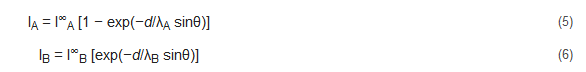
IA and IB are the detected intensities deriving from A and B, I∞A and I∞B are the signal intensities that would be generated by a sample formed just by A and B and λA and λB are their attenuation lengths. θ is the take-off angle defined by the sample surface and the analyzer axis. By applying Equations (5) and (6), the authors obtained λ values expressed in monolayers. Using a “universal curve”, the authors fitted the values of the attenuation length separately for elements and organic and inorganic compounds. The general form of the universal curve is

For energies between 1 and 10,000 eV above the Fermi level, a = 538, b = 0.41 and d is the thickness of the monolayer, expressed as

Here, A is the atomic or molecular weight, n is the number of atoms in the molecule, N is Avogadro’s number and ρ is the bulk density in kg m−3. Fitting Equation (9) for inorganic compounds gives a = 2170 and b = 0.72, while for organic molecules, a = 49 and b = 0.11.
The trend of the attenuation length as a function of the energy can be utilized to vary the sampling depth, which is commonly taken as 3λ. The photon energy varies from few eV when using ultraviolet sources (generally, He sources emitting HeI at 21.2 eV and HeII at 40.8 eV photons) to 1253.6 eV or 1486.6 eV for Mg and Al Kα anodes, which are generally utilized in the X-ray sources of XPS instruments. Using synchrotrons to perform photoelectron spectroscopy, the radiation energy is varied in a broad range from 10 to 104 eV. Then, the sampling depth varies from fractions of nanometers when using UV to some nanometers in the case of X-ray photons or up to ~20 nm using hard X-ray photons (depending on the material).
4. Angle-Resolved XPS
The attenuation of the photocurrent described by the Lambert–Beer law (4) enables the non-destructive depth profiling of the sample surface. Equations (5) and (6) describe the variation of the electron photocurrent as a function of the attenuation length and the take-off angle. In a simple case, it is possible to analyze the changes of different “bond-components” of a core line by varying the take-off angle. A well-known example is the estimate of the thickness of silicon native oxide. Equations (5) and (6) are reduced to

To make the effect of the tilt clearer, the spectra are normalized to a common intensity. As can clearly be seen, increasing the tilt angle increases the intensity of the silicon oxide at ~103 eV. Applying Equation (9) it is possible to estimate the thickness of the native oxide, which is ~0.4 nm.
References
- Egelhoff, W.F. Core-level binding-energy shifts at surfaces and in solids. Surf. Sci. Rep. 1987, 6, 253–451.
- Schattke, W.; van Hove, M.A. Solid-State Photoemission and Related Methods: Theory and Experiment; Wiley: Weinheim, Germany, 2003.
- Miron, C.; Morin, P. Handbook of High-Resolution Spectroscopy; John Wiley & Sons, Ltd.: New York, NY, USA, 2011.
- Susi, T.; Pichler, T.; Ayala, P. X-ray photoelectron spectroscopy of graphitic carbon nanomaterials doped with heteroatoms. Beilstein J. Nanotechnol. 2015, 6, 177–192.
- Weiland, C.; Rumaniz, A.K.; Pianetta, P.; Woicik, J.C. Recent applications of hard X-ray photoelectron spectroscopy. J. Vac. Sci. Technol. A 2016, 34, 030801.
- Nordling, C.; Sokolowski, E.; Siegbahn, K. Precision Method for Obtaining Absolute Values of Atomic Binding Energies. Phys. Rev. 1957, 105, 1676.
- Fadley, C.S. X-ray photoelectron spectroscopy: From origins to future directions. Nucl. Instrum. Methods Phys. Res. A 2009, 601, 8–39.
- Hill, J.P. Ultraviolet Photoelectron Spectroscopy. In Characterization of Materials; Kaufmann, E.N., Ed.; John Wiley & Sons, Inc.: Hoboken, NJ, USA, 2003.
- Rabalais, J.W. Principles of Ultraviolet Photoelectron Spectroscopy; Wiley-Interscience: New York, NY, USA, 1977.
- Powell, C.J.; Seah, M.P. Precision, accuracy, and uncertainty in quantitative surface analyses by Auger-electron spectroscopy and X-ray photoelectron spectroscopy. J. Vac. Sci. Technol. A 1990, 8, 735.
- Tilinin, I.S.; Jablonski, A.; Werner, W.S.M. Quantitative surface analysis by Auger and X-ray photoelectron spectroscopy. Prog. Surf. Sci. 1996, 52, 193–335.
- Seah, M.P. Quantification of AES and XPS. In Practical Surface Analysis Vol. 1 Auger and X-ray Photoelectron Spectroscopy; Briggs, D., Seah, M.P., Eds.; J. Wiley & Sons: Chichester, UK, 1990; pp. 206–251.
- Fadley, C.S. X-ray photoelectron spectroscopy: Progress and perspectives. J. Electron Spectrosc. Relat. Phenom. 2010, 178–179, 2–32.
- Reilman, R.F.; Msezane, A.; Manson, S.T. Relative intensities in photoelectron spectroscopy of atoms and molecules. J. Electron Spectrosc. Relat. Phenom. 1976, 8, 389–394.
- Scofield, J.H. Hartree-Slater subshell photoionization cross-sections at 1254 and 1487 eV. J. Electron Spectrosc. Relat. Phenom. 1976, 8, 129–137.
- Wagner, C.D.; Davis, L.E.; Zeller, M.V.; Taylor, J.A.; Raymond, R.H.; Gale, L.H. Empirical atomic sensitivity factors for quantitative analysis by electron spectroscopy for chemical analysis. Surf. Interface Anal. 1981, 3, 211–225.
- Brundle, C.R.; Crist, B.V. X-ray photoelectron spectroscopy: A perspective on quantitation accuracy for composition analysis of homogeneous materials. J. Vac. Sci. Technol. A 2020, 38, 041001.
- Briggs, D. Surface Analysis of Polymers by XPS and Static SIMS; Cambridge University Press: Cambridge, UK, 1998.
- Seah, M.P.; Dench, W.A. Quantitative electron spectroscopy of surfaces: A standard data base for electron inelastic mean free paths in solids. Surf. Interface Anal. 1979, 1, 2–11.
More
Information
Subjects:
Spectroscopy
Contributor
MDPI registered users' name will be linked to their SciProfiles pages. To register with us, please refer to https://encyclopedia.pub/register
:
View Times:
1.4K
Revision:
1 time
(View History)
Update Date:
02 Jul 2022
Table of Contents


Notice
You are not a member of the advisory board for this topic. If you want to update advisory board member profile, please contact office@encyclopedia.pub.
OK
Confirm
Only members of the Encyclopedia advisory board for this topic are allowed to note entries. Would you like to become an advisory board member of the Encyclopedia?
Yes
No
${ textCharacter }/${ maxCharacter }
Submit
Cancel
Back
Comments
${ item }
|
${ item.createdUser.fullName }
${ item.createdAt }
${ item.vote }
${ item.reply }
Delete
${ reply.createdUser.fullName }
${ reply.createdAt }
${ reply.vote }
Delete
There is no reply to this comment~
${ item.replyTextCharacter }/${ item.replyMaxCharacter }
Submit
Cancel
More
No more~
There is no comment~
${ textCharacter }/${ maxCharacter }
Submit
Cancel
${ selectedItem.replyTextCharacter }/${ selectedItem.replyMaxCharacter }
Submit
Cancel
Confirm
Are you sure to Delete?
Yes
No