Your browser does not fully support modern features. Please upgrade for a smoother experience.
Submitted Successfully!
 +1 credit
Thank you for your contribution! You can also upload a video entry or images related to this topic.
For video creation, please contact our Academic Video Service.
| Version | Summary | Created by | Modification | Content Size | Created at | Operation |
|---|---|---|---|---|---|---|
| 1 | Björn Gojdka | -- | 3023 | 2022-04-15 08:37:25 | | | |
| 2 | Conner Chen | Meta information modification | 3023 | 2022-04-15 08:56:35 | | |
Video Upload Options
We provide professional Academic Video Service to translate complex research into visually appealing presentations. Would you like to try it?
Cite
If you have any further questions, please contact Encyclopedia Editorial Office.
Gojdka, B. Applications of the PowderMEMS Microstructures. Encyclopedia. Available online: https://encyclopedia.pub/entry/21811 (accessed on 24 June 2026).
Gojdka B. Applications of the PowderMEMS Microstructures. Encyclopedia. Available at: https://encyclopedia.pub/entry/21811. Accessed June 24, 2026.
Gojdka, Björn. "Applications of the PowderMEMS Microstructures" Encyclopedia, https://encyclopedia.pub/entry/21811 (accessed June 24, 2026).
Gojdka, B. (2022, April 15). Applications of the PowderMEMS Microstructures. In Encyclopedia. https://encyclopedia.pub/entry/21811
Gojdka, Björn. "Applications of the PowderMEMS Microstructures." Encyclopedia. Web. 15 April, 2022.
Copy Citation
PowderMEMS is a powder-based microfabrication technology for substrate-level integration of three-dimensional functional microstructures into MEMS devices. The wide choice of materials and customizable properties opens a multitude of applications for the PowderMEMS technology. Next to the shape and volume of the 3D structure itself, additional application-specific physical and chemical characteristics can be controlled by choice of the particles and the ALD layer
Applications
PowderMEMS
1. Magnetic Applications
By choosing magnetic particles, PowderMEMS can be used to create integrated microstructures with magnetic properties without the harsh temperatures required for sintering, while also providing the magnetic particles with a passivating ALD layer. These precisely defined structures can therefore be directly integrated into MEMS at the wafer level, replacing cumbersome and expensive hybrid integration of magnetic materials at the chip level. More information on the general usage of micromagnets in MEMS applications can be found in [1].
1.1. Integrated Permanent Magnets
High-power permanent micromagnets are of interest for MEMS actuators as well as for sensors. However, until now, a suitable fabrication method at the wafer level that is BEOL-compatible was not available. Figure 1 presents photographs of integrated NdFeB micromagnets created using PowderMEMS. Figure 1a shows an 8-inch Si substrate with micromagnets of various designs. Figure 1b shows triangular silicon frames with micromagnets in the corners, sticking magnetically together and to a metal plate. Magnetization of the micromagnets was performed out of plane at the wafer level with a magnetic field of 3.5 T on a custom 8” wafer magnetization tool.
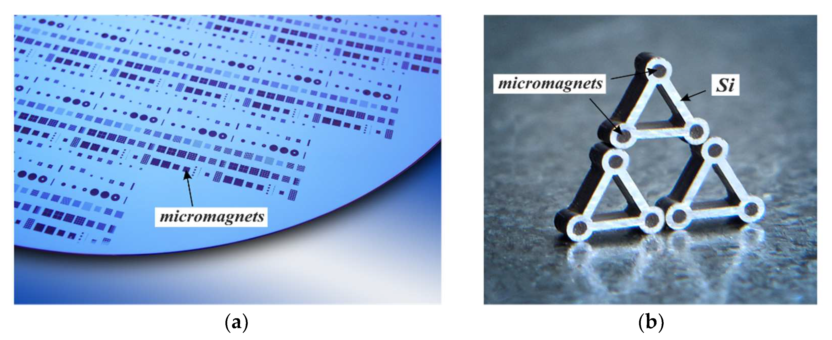
Figure 1. (a) PowderMEMS micromagnets fabricated from NdFeB powder inside an 8” wafer. (b) Triangular Si frames with magnetized NdFeB micromagnets in the corners, magnetically sticking together and to the underlying metal plate. The Si is ~700 µm thick; the micromagnets are 300 µm in diameter and extend ~600 µm into the Si.
1.2. Energy Harvesting
Figure 2 depicts piezoelectric vibrational energy harvesters with an integrated micromagnet array as a movable tip mass. With such a device, electrical energy can be generated by mechanical excitations—e.g., vibrations and shocks—as well as from time-varying external magnetic fields using magnetic force coupling [2][3]. Two major advantages can be identified compared to devices with conventional silicon-based tip mass: Firstly, increased seismic masses lead to lower resonance frequencies, which better match to the sources of mechanical vibrations available in the environment. Secondly, with a magnet as the seismic mass, energy can be harvested contactlessly from rotational and translational motions. The available magnetic forces are often equivalent to an acceleration of several tens of g’s, if compared to mechanical excitation. Thus, frequency upconversion from both strong mechanical as well as magnetic-pulse-like excitations can be utilized, making it possible to harvest energy at low excitation frequencies of <50 Hz with power outputs of >70 µW [4]. Notably, it was further demonstrated that the generated power is sufficient to switch an NMOS and to initiate near-zero-power wake-up [5]. Apart from that, magnetic field detection with an ultralow limit of detection of 7.2 pT/Hz0.5–8.5 pT/Hz0.5 in resonance has been demonstrated [6].

Figure 2. (a) Wafer with piezoelectric vibrational harvesters with integrated micromagnet arrays. (b) Detailed views of a single energy harvester from the top (lower left) and the bottom (upper left), as well as a packaged device.
1.3. Inductors
MEMS inductors with a soft magnetic 3D core are without doubt indispensable for future power electronics. Cores based on PowderMEMS 3D microstructures, as exemplarily shown in Figure 3, were described for the first time in [7]. The impact of different soft magnetic powders was evaluated, and a boost converter with a GaN FET was developed to prove the functionality of the PowderMEMS inductors using a demonstrator with manually wound wire. At 20 MHz, an input voltage of 15 V could be boosted to 25 V on the output at a load current of 481 mA with an efficiency of 87%. It is expected that cores based on porous 3D microstructures will exhibit an outstandingly high thermal stability since, in contrast to other powder-based techniques, no organic materials are involved in the fabrication process and, consequently, in the core.
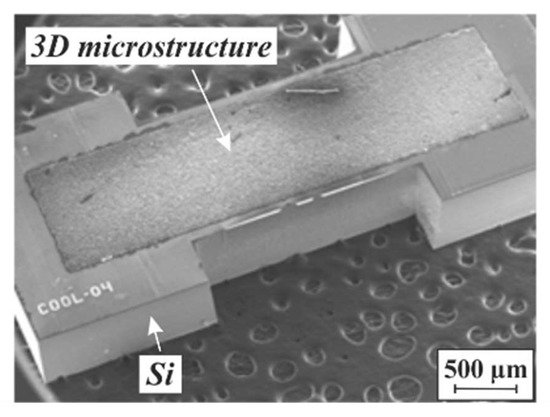
Figure 3. SEM micrograph of a soft magnetic PowderMEMS core for MEMS inductors, agglomerated from Fe particles by 75 nm ALD-Al2O3 at 75 °C.
2. Optical Applications
Since the very thin ALD layers used for PowderMEMS are typically optically transparent, incident light can easily penetrate deep into a 3D microstructure made from transparent particles. By using optically active particles, this feature can be exploited to develop innovative optical MEMSs.
A first evaluation of pixelated MEMS luminescence converter arrays for laser-based lighting applications, agglomerated from phosphor particles, has been previously described (Figure 4) [8]. For a general description of this lighting principle, the reader is referred to [9]. The quantum efficiency was found to be ~95% in the investigated blue spectral range, which is a value comparable to commercial phosphor converters. A unique feature is the high optical contrast between illuminated and non-illuminated adjacent pixels, differing by around two orders of magnitude. Since all pixels are separated from one another by the substrate material, the light scattering from illuminated pixels into the neighboring ones (optical crosstalk) is strongly suppressed.
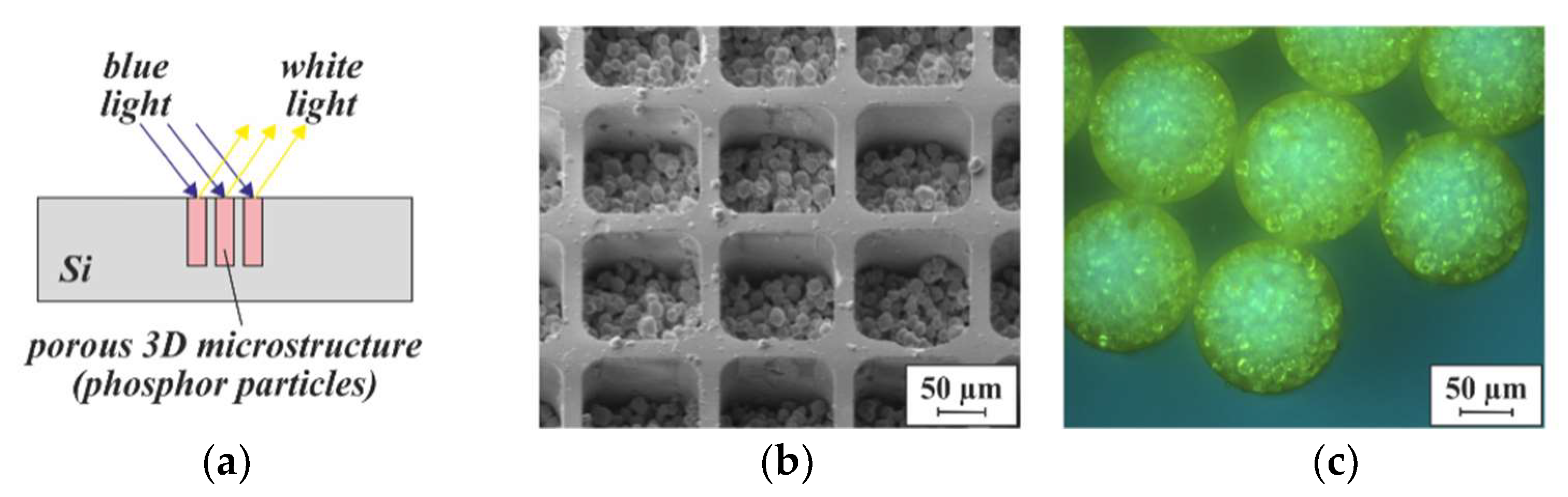
Figure 4. (a) Schematic illustration of a PowderMEMS luminescence converter based on agglomerated phosphor particles [8]. (b) SEM micrograph of the top side of a converter array, consisting of square-shaped pixels. (c) Optical image of the bottom side of another converter array, consisting of circular pixels, after removal of the Si substrate by etching in XeF2 vapor.
3. Thermal Applications
The tunable intrinsic porosity of PowderMEMS structures can be exploited for both cooling and thermal insulation of MEMSs. Cooling can be typically achieved by flowing a coolant through a 3D microstructure made from particles with high thermal conductivity. On the other hand, if particles with low thermal conductivity are chosen, thermally insulating structures can be realized in MEMSs.
3.1. Cooling of MEMSs
Porous 3D microstructures, whose particles generate heat during operation, can be actively cooled by a fluid flowing through the structure. In Figure 5a, this concept is illustrated for the case of a luminescence converter. As already demonstrated, even a slow air flow causes a considerable decrease in the phosphor temperature [8]. With optimized converter geometry and a suitable cooling fluid, the light density of luminescence converters, commonly limited by thermal quenching of the phosphor, could be increased significantly.

Figure 5. Concepts for actively cooled MEMSs: A coolant is forced through (a) a porous luminescence converter, manufactured from phosphor particles, and (b) a porous 3D microstructure, manufactured from particles with high thermal conductivity, which is embedded in a Si chip with a heat-generating electronic device.
Apart from luminescence converters, porous 3D microstructures agglomerated from particles with high thermal conductivity—such as Si or diamond—could be of interest for active cooling of electronic devices (see Figure 5b). In [10] it is shown that the cooling of a heat source by a fluid, flowing through a channel close to the heat source, is improved by a porous medium within this channel. In [11], the thermal conductivity of the underfill between stacked chips is improved by loading the gap with particles with high thermal conductivity prior to the application of the underfill material. Similar features can be achieved with PowderMEMS, in a manner well compatible with most other MEMS processes.
3.2. Thermal Insulation
The cumulative thermal conductivity of a porous structure is the sum of the thermal conductivities of the solid structure and the fluid contained within the pores. In a dry system of solid particles and gas, the gaseous phase controls the overall effective thermal conductivity [12]. The heat transfer from particle to particle is strongly hindered, since the area of the point-type contacts between neighboring particles is very small compared to the particle surface, which is in contact with the gas. The effective thermal conductivity can be further decreased by one order of magnitude if the pressure of the gas within the pores is reduced below 1 mbar [12]. Similar pressure values are common working points for plasma-enhanced chemical vapor deposition (PECVD) processes. Accordingly, with optimized geometry and optimal particles, porous 3D microstructures with outstandingly low effective thermal conductivity can be generated using standard MEMS fabrication processes.
Figure 6 illustrates two possible concepts schematically. A finished conventional device, comprising a thin membrane with a heater, electrically connected to bond pads, can be equipped with a porous 3D microstructure from its backside. Subsequent deposition of a sealing layer on the backside—for example, by PECVD—ensures reduced pressure (vacuum) inside it (Figure 6a). Alternatively, the porous 3D microstructure can be realized first; after its planarization and sealing under vacuum, the MEMS device is post-processed on top of the substrate (Figure 6b). This second approach completely replaces the need for a membrane, and would provide a thermally insulating, mechanically robust support that is expected to have a lower failure rate during substrate processing than stress-compensated thin-film membranes, as well as much higher resistivity to overpressure and shocks of the fabricated MEMS device during operation. Moreover, post-processing of through-silicon vias could be used to separate the electrical contacts (bond pads) from the sensing environment by relocating them to the backside of the substrate.
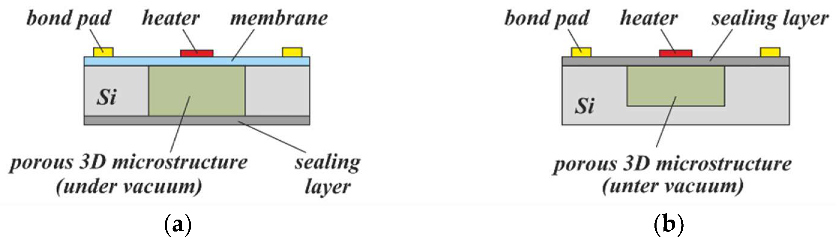
Figure 6. Concepts for the thermal insulation of calorimetric MEMS devices using porous 3D microstructures under vacuum: In (a) the 3D microstructure is post-processed within the backside cavity of a finished, membrane-based device and, finally, sealed under vacuum. In (b), the 3D microstructure is pre-processed including planarization and sealing under vacuum. Subsequently, the MEMS device is processed on top. Please note that in both cross-sections the electrical wiring from the heater to the bond pads is not shown.
4. Porous Solid Phases for Microfluidic Applications
A multitude of microfluidic applications can take advantage of the large inner surface area and irregular channel network of PowderMEMS microstructures. The two most basic use cases are as integrated filters for particle retention in fluidic streams, and to enhance the mixing of two or more fluids. Mixing has been shown to greatly benefit from porous microstructures for turbulence induction in low-Reynolds-number flow, thereby shortening the mixing length and reducing mixing time [13][14].
The very large inner surface area of PowderMEMS structures can be used as a solid phase for the adsorption or immobilization of molecules. Typical examples include their use in microfluidic devices for nucleic acid purification via solid-phase extraction, or in devices for miniaturized chromatography [15]. Figure 7 shows a photo of a Si substrate with 20 mm long, meandrous porous structures for on-chip liquid chromatography agglomerated from oxidized SiO2 beads with ALD-Al2O3. Following the structural agglomeration, SiO2 was deposited by ALD in the same way to achieve an inner surface suitable for hydrophilic interaction liquid chromatography (HILIC). On-chip separation of a mixture of acetaminophen and gentisic acid was successfully demonstrated [2]. Furthermore, the BEOL compatibility of the PowderMEMS process makes it possible to integrate electrochemical or optical detectors for the direct measurement of the eluted target substances with the microscale chromatography column, forming a complete analysis chip.

Figure 7. Silicon substrate with 20 mm long, meander-type porous 3D microstructures, agglomerated from monodisperse oxidized Si beads with a mean size of 10 µm using 75 nm ALD-Al2O3.
Porous solid phases also have important applications in chemical synthesis as a support for immobilized molecules and catalytic surfaces. An example for the immobilization of molecules is the synthesis of nucleic acids in microfluidic devices, where the growing DNA or RNA strand is immobilized on a porous solid support [16].
Very large catalytic surfaces can be achieved by coating the inner surface of a porous 3D microstructure with catalytically active ALD layers such as TiO2 or Pt. Here, a key advantage of PowderMEMS is that further properties of the support material can be chosen freely. For example, by selecting an optically transparent powder that is embedded in an optically transparent microchannel, photocatalytic microreactors can be developed that offer even larger catalytic surfaces than those that are achievable by deposition of the catalytic surface on the channel walls alone [17]. To achieve even more complex (organic) catalysts, the surface may then be further modified by the use of molecular layer deposition (MLD) techniques [18]. As MLD can be performed using the same equipment as ALD, PowderMEMS has the unique advantage that both the formation of the porous support framework and the deposition of highly complex catalytic surfaces can be performed as sequential processes in the same reactor.
5. Sensors
5.1. Flow Sensors
Calorimetric flow sensors and pyroelectric sensors commonly use thin-film membranes to achieve thermal insulation of the sensing elements from the bulk substrate [19][20]. For a general description of this type of sensor, the reader is referred to [21]. These membranes are very fragile, which leads to difficulties during sensor fabrication, as well as a high risk of catastrophic failure due to overpressure or physical shock. As already described in Section 4.3.2, PowderMEMS can be used to improve upon existing sensor designs via the formation of a porous 3D microstructure with very low thermal conductivity within the cavity below the membrane (see Figure 6a). Apart from a better mechanical stability in such a way, parasitic effects such as air convection within the backside volume—causing a distortion of the sensor signal—can be suppressed. Enhanced sensing performance is expected in fluids with high thermal conductivity.
A first proof of the thermal insulation properties of porous 3D microstructures, fabricated from particles of different materials using flow sensor designs, is exemplarily shown in Figure 8. Please note that in contrast to Figure 6a, the porous 3D microstructure remained unsealed from the backside in order to allow a variation in the gas pressure within the pores.
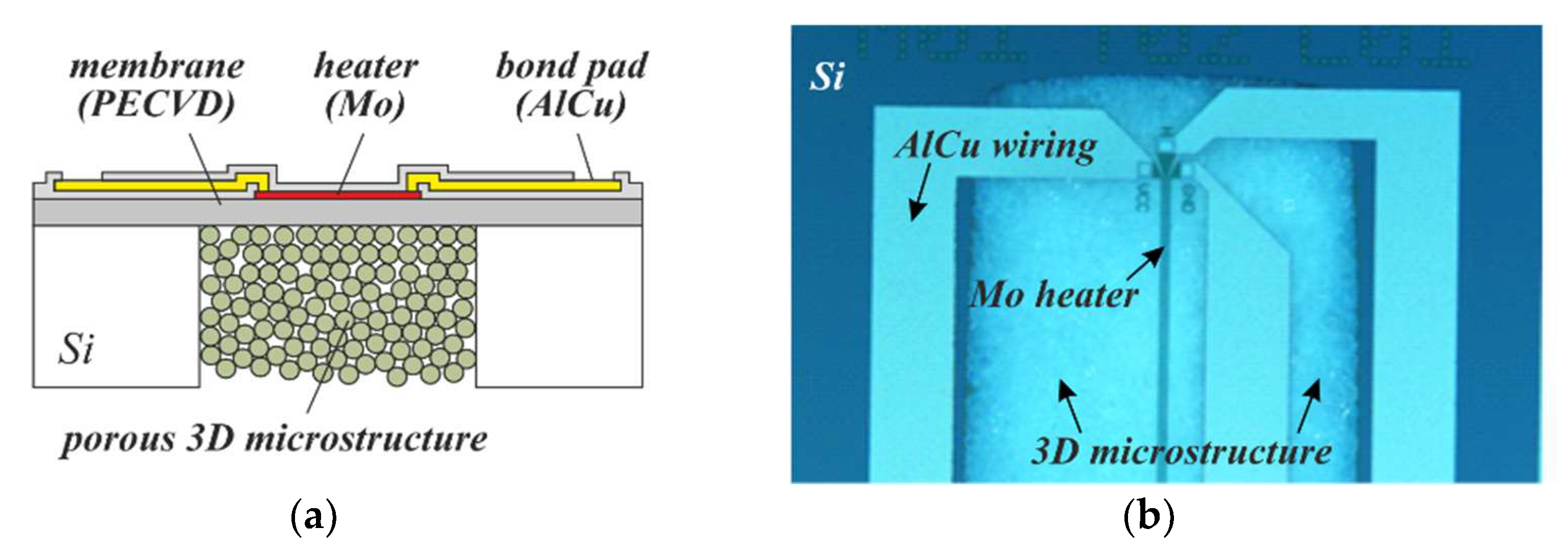
Figure 8. (a) Cross-section of a thin-film-membrane-based calorimetric flow sensor, whose backside cavity has been equipped with a 3D microstructure at the wafer level. (b) Optical image of the top side of a particular sensor design. The 3D microstructure can be seen through the transparent membrane.
5.2. Gas Sensors
Since wafers with embedded porous 3D microstructures can be post-processed using common MEMS and semiconductor processes, there are different ways to integrate heaters and electrodes on top, nearby, or even within them. A porous 3D microstructure modified by ALD with a semiconductive gas-sensitive layer such as TiO2 can thus be both contacted electrically as well as heated to form a catalytic gas sensor (Figure 9a). For a general description of this type of sensor, the reader is referred to [22]. As is known, the activation energy for the gas-sensitive layer can also be delivered via optical excitation. PowderMEMS offers the unique advantage of using optically transparent particles to obtain the 3D microstructure supporting the catalytic layer [23]. In this way, deep penetration of light into the gas-sensitive structure can be achieved, which is expected to improve the sensitivity (Figure 9b).
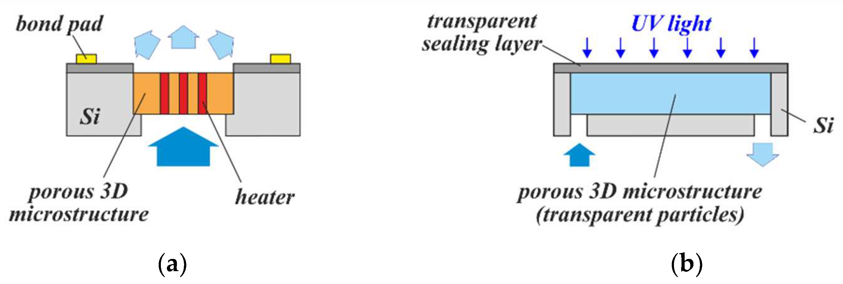
Figure 9. Concepts for PowderMEMS gas sensors: (a) Resistive heating of the catalyst. (b) Optical activation of the catalyst.
Other types of gas sensors could also benefit from the PowderMEMS process. For example, existing paramagnetic oxygen sensors, which rely on macroscale hybrid integration of rare-earth magnets, could be modified to include micromagnets that are integrated at the wafer level, making the post-processing of single chips and hybrid mounting of conventional magnets unnecessary [24].
Another promising application that is relevant for gas sensors is their protection from dust or moisture. Several groups have shown this principle at the chip- or package level, demonstrating that very thin structures that are still mechanically robust are needed in order to prevent unacceptable delays in sensor response [25][26]. With PowderMEMS, thin, microporous, protective caps can be fabricated at the wafer level and integrated with the MEMS devices using common wafer-level bonding techniques (Figure 10). If necessary, the cap wafer can be provided with moisture protection by depositing a corresponding material on its top side before or after bonding.

Figure 10. (a) Concept of an environmental protection cap for gas sensors, which must communicate with the environment, but degrades if contaminated with particles or moisture; (b) illustration of their integration with sensors by wafer-level packaging.
5.3. Electrochemistry and Biosensors
Electrodes for electrochemical applications benefit from large surface areas. For a general description of this type of sensor and its applications, the reader is referred to [27]. With PowderMEMS, there are two possible ways to manufacture high-surface-area electrodes: The first way is ALD of a catalytic material such as Pt onto the inner surface of the porous structure (Figure 11a); however, ALD processes for the deposition of precious metals often use expensive precursors, and are difficult to control [28]. The second strategy is the formation of a powder-based electrode via physical retention of a conductive, catalytic powder inside an etched microcavity on top of a thin-film electrode [29][30]. The retention can be achieved via partial agglomeration of the powder inside the cavity, essentially forming a porous plug on top of the loose powder (Figure 11b), as has already been demonstrated in [31]. A further advantage of this type of electrode is its self-wicking behavior, which enables passive filling of the electrode cavity.

Figure 11. Concepts for large-surface-area electrodes manufactured via the PowderMEMS process: (a) Electrode formed by coating of the porous structure with a conductive ALD layer. (b) Electrode formed by confining a loose conductive powder inside a cavity.
A porous microstructure can also be used as a solid support for the immobilization of biomolecules such as enzymes or antibodies. Hereby, the sensitivity of biosensors can be improved by providing a much larger surface for interaction between the sample containing the target molecules and the immobilized, captured molecules [32][33][34].
Another concept is the utilization of thin-film electrodes, deposited onto a 3D microstructure, for electrochemical sensing. The irregular, rough surface of the 3D microstructure not only causes an effective increase in the electrode area—open “undercut” pores remain within the metal layer due to the limited step coverage of deposition processes such as sputtering or evaporation, so that a fluid can be passed through both the porous 3D microstructure as well as the thin-film electrode on top. In this way, in contrast to common planar arrangements, the entire fluid volume contacts the electrode. Figure 12 illustrates this novel type of flow-through 3D sensor schematically, and presents an SEM micrograph of such a structure from the top side.

Figure 12. (a) Schematic concept of a flow-through 3D sensor with a thin-film electrode deposited on top of a porous 3D microstructure, and (b) SEM micrograph of the top side of such a structure. The electrode consists of sputtered Au. The porous 3D microstructure, 500 µm in diameter and ~500 µm deep, was agglomerated from 5 µm NdFeB particles by 75 nm ALD-Al2O3.
References
- Jackson, N.; Pedrosa, F.J.; Bollero, A.; Mathewson, A.; Olszewski, O.Z. Integration of Thick-Film Permanent Magnets for MEMS Applications. J. Microelectromechanical Syst. 2016, 25, 716–724.
- Behrmann, O.; Lisec, T.; Piechotta, G.; Gojdka, B. A microfluidic porous solid phase suitable for mass production. MikroSystemTechnik Kongr. 2021, 2021, 446–449.
- Cook-Chennault, K.A.; Thambi, N.; Sastry, A.M. Powering MEMS portable devices—a review of non-regenerative and regenerative power supply systems with special emphasis on piezoelectric energy harvesting systems. Smart Mater. Struct. 2008, 17, 43001.
- Lofink, F.; Tolstrup, V.; Lisec, T.; Reimer, T.; Piorra, A.; Meyners, D.; Quandt, E.; Wagner, B. Magnetically driven energy-harvester with monolithically integrated high-energy-density magnets. In Proceedings of the 2017 19th International Conference on Solid-State Sensors, Actuators and Microsystems, Kaohsiung, Taiwan, 18–22 June 2017.
- Gojdka, B.; Dankwort, T.; Nowak, M.A.; Bodduluri, M.T.; Ahmed, M.; Grunzig, S.; Lofink, F. Magnetically Excited Piezoelectric Energy Harvester for Micropower Supply and Wakeup Applications. In Proceedings of the 2021 21st International Conference on Solid-State Sensors, Actuators and Microsystems (Transducers), Orlando, FL, USA, 20–25 June 2021; pp. 455–458.
- Niekiel, F.; Su, J.; Bodduluri, M.T.; Lisec, T.; Blohm, L.; Pieper, I.; Wagner, B.; Lofink, F. Highly sensitive MEMS magnetic field sensors with integrated powder-based permanent magnets. Sens. Actuators A: Phys. 2019, 297, 111560.
- Paesler, M.; Lisec, T.; Kapels, H. Novel Integrated BEOL Compatible Inductances for Power Converter Applications. In Proceedings of the 2020 IEEE Applied Power Electronics Conference and Exposition (APEC), New Orleans, LA, USA, 15–19 March 2020; pp. 2647–2652.
- Steudel, F.; Lisec, T.; Nolte, P.W.; Hofmann, U.; Wantoch, T.; Lofink, F.; Schweizer, S. Pixelated phosphors for high-resolution and high-contrast white light sources. Opt. Express 2018, 26, 26134–26144.
- Peng, Y.; Mou, Y.; Wang, H.; Zhuo, Y.; Li, H.; Chen, M.; Luo, X. Stable and efficient all-inorganic color converter based on phosphor in tellurite glass for next-generation laser-excited white lighting. J. Eur. Ceram. Soc. 2018, 38, 5525–5532.
- Chen, C.-C.; Huang, P.-C.; Hwang, H.-Y. Enhanced forced convective cooling of heat sources by metal-foam porous layers. Int. J. Heat Mass Transf. 2013, 58, 356–373.
- Zimmermann, S.; Brunschwiler, T.; Burg, B.R.; Zuercher, J.; Hong, G.; Poulikakos, D.; Baum, M.; Hofmann, C. Characterization of particle beds in percolating thermal underfills based on centrifugation. 2014 Int. 3d Syst. Integr. Conf. (3dic) 2014, 122014, 1–7.
- Huetter, E.S.; Koemle, N.I.; Kargl, G.; Kaufmann, E. Determination of the effective thermal conductivity of granular materials under varying pressure conditions. J. Geophys. Res. Earth Surf. 2008, 113, 113.
- Rohr, T.; Yu, C.; Davey, M.H.; Svec, F.; Fréchet, J.M.J. Porous polymer monoliths: Simple and efficient mixers prepared by direct polymerization in the channels of microfluidic chips. Electrophor. 2001, 22, 3959–3967.
- Xiao, Z.; Wang, A.; Perumal, J.; Kim, N.-P. Facile Fabrication of Monolithic 3D Porous Silica Microstructures and a Microfluidic System Embedded with the Microstructure. Adv. Funct. Mater. 2010, 20, 1473–1479.
- Boom, R.; Sol, C.J.; Salimans, M.M.; Jansen, C.L.; Dillen, P.M.W.-V.; van der Noordaa, J. Rapid and simple method for purification of nucleic acids. J. Clin. Microbiol. 1990, 28, 495–503.
- Huang, Y.; Castrataro, P.; Lee, C.-C.; Quake, S.R. Solvent resistant microfluidic DNA synthesizer. Lab Chip 2007, 7, 24–26.
- Krivec, M.; Žagar, K.; Suhadolnik, L.; Čeh, M.; Dražić, G. Highly Efficient TiO2-Based Microreactor for Photocatalytic Applications. ACS Appl. Mater. Interfaces 2013, 5, 9088–9094.
- Meng, X. An overview of molecular layer deposition for organic and organic–inorganic hybrid materials: Mechanisms, growth characteristics, and promising applications. J. Mater. Chem. A 2017, 5, 18326–18378.
- Gardner, E.L.W.; Vincent, T.A.; Jones, R.G.; Gardner, J.W.; Coull, J.; De Luca, A.; Udrea, F. MEMS Thermal Flow Sensors— An Accuracy Investigation. IEEE Sens. J. 2019, 19, 2991–2998.
- Dao, T.D.; Ishii, S.; Doan, A.T.; Wada, Y.; Ohi, A.; Nabatame, T.; Nagao, T. An On-Chip Quad-Wavelength Pyroelectric Sensor for Spectroscopic Infrared Sensing. Adv. Sci. 2019, 6, 1900579.
- Ejeian, F.; Azadi, S.; Razmjou, A.; Orooji, Y.; Kottapalli, A.; Warkiani, M.E.; Asadnia, M. Design and applications of MEMS flow sensors: A review. Sens. Actuators A: Phys. 2019, 295, 483–502.
- Asri, M.I.A.; Hasan, N.; Fuaad, M.R.A.; Yunos, Y.M.; Ali, M.S.M. MEMS Gas Sensors: A Review. IEEE Sens. J. 2021, 21, 18381–18397.
- Xu, F.; Ho, H.-P. Light-Activated Metal Oxide Gas Sensors: A Review. Micromachines 2017, 8, 333.
- Vonderschmidt, S.; Müller, J. A fluidic bridge based MEMS paramagnetic oxygen sensor. Sens. Actuators B: Chem. 2013, 188, 22–30.
- Dean, R.N.; Surgnier, S.; Pack, J.; Sanders, N.; Reiner, P.; Long, C.W.; Fenner, R.; Fenner, W.P. Porous Ceramic Packaging for a MEMS Humidity Sensor Requiring Environmental Access. IEEE Trans. Compon. Packag. Manuf. Technol. 2011, 1, 428–435.
- Ma, Y.; Kaczynski, J.; Ranacher, C.; Roshanghias, A.; Zauner, M.; Abasahl, B. Nano-porous aluminum oxide membrane as filtration interface for optical gas sensor packaging. Microelectron. Eng. 2018, 198, 29–34.
- Tabata, M.; Miyahara, Y. From new materials to advanced biomedical applications of solid-state biosensor: A review. Sens. Actuators B: Chem. 2021, 352, 131033.
- Mäkelä, M.; Hatanpää, T.; Mizohata, K.; Räisänen, J.; Ritala, M.; Leskelä, M. Thermal Atomic Layer Deposition of Continuous and Highly Conducting Gold Thin Films. Chem. Mater. 2017, 29, 6130–6136.
- Cha, C.; Li, C.M.; Yang, H.; Liu, P. Powder microelectrodes. J. Electroanal. Chem. 1994, 368, 47–54.
- Cachet-Vivier, C.; Vivier, V.; Cha, C.; Nedelec, J.-Y.; Yu, L. Electrochemistry of powder material studied by means of the cavity microelectrode (CME). Electrochim. Acta 2001, 47, 181–189.
- Chemnitz, S.; Reimer, T.; Lisec, T. Herstellung neuartiger Mikrostrukturen für MEMS-Anwendungen durch Pulververfestigung mittels ALD. In Proceedings of the MikroSystemTechnik Kongress, München, Germany, 23–25 October 2017.
- Armbrecht, L.; Dincer, C.; Kling, A.; Horak, J.; Kieninger, J.; Urban, G. Self-assembled magnetic bead chains for sensitivity enhancement of microfluidic electrochemical biosensor platforms. Lab Chip 2015, 15, 4314–4321.
- Shin, K.-S.; Lee, S.W.; Han, K.-C.; Kim, S.K.; Yang, E.K.; Park, J.H.; Ju, B.-K.; Kang, J.Y.; Kim, T.S. Amplification of fluorescence with packed beads to enhance the sensitivity of miniaturized detection in microfluidic chip. Biosens. Bioelectron. 2007, 22, 2261–2267.
- Yang, Y.-N.; Lin, H.-I.; Wang, J.-H.; Shiesh, S.-C.; Lee, G.-B. An integrated microfluidic system for C-reactive protein measurement. Biosens. Bioelectron. 2009, 24, 3091–3096.
More
Information
Subjects:
Materials Science, Composites
Contributor
MDPI registered users' name will be linked to their SciProfiles pages. To register with us, please refer to https://encyclopedia.pub/register
:
View Times:
1.0K
Revisions:
2 times
(View History)
Update Date:
15 Apr 2022
Table of Contents


Notice
You are not a member of the advisory board for this topic. If you want to update advisory board member profile, please contact office@encyclopedia.pub.
OK
Confirm
Only members of the Encyclopedia advisory board for this topic are allowed to note entries. Would you like to become an advisory board member of the Encyclopedia?
Yes
No
${ textCharacter }/${ maxCharacter }
Submit
Cancel
Back
Comments
${ item }
|
${ item.createdUser.fullName }
${ item.createdAt }
${ item.vote }
${ item.reply }
Delete
${ reply.createdUser.fullName }
${ reply.createdAt }
${ reply.vote }
Delete
There is no reply to this comment~
${ item.replyTextCharacter }/${ item.replyMaxCharacter }
Submit
Cancel
More
No more~
There is no comment~
${ textCharacter }/${ maxCharacter }
Submit
Cancel
${ selectedItem.replyTextCharacter }/${ selectedItem.replyMaxCharacter }
Submit
Cancel
Confirm
Are you sure to Delete?
Yes
No