Your browser does not fully support modern features. Please upgrade for a smoother experience.
Submitted Successfully!
 +1 credit
Thank you for your contribution! You can also upload a video entry or images related to this topic.
For video creation, please contact our Academic Video Service.
| Version | Summary | Created by | Modification | Content Size | Created at | Operation |
|---|---|---|---|---|---|---|
| 1 | Gookbin CHO | + 4968 word(s) | 4968 | 2022-01-05 09:30:37 | | | |
| 2 | Dean Liu | -9 word(s) | 4959 | 2022-02-10 07:31:25 | | |
Video Upload Options
We provide professional Academic Video Service to translate complex research into visually appealing presentations. Would you like to try it?
Cite
If you have any further questions, please contact Encyclopedia Editorial Office.
Cho, G. CNT-Based Chemical Sensors. Encyclopedia. Available online: https://encyclopedia.pub/entry/19301 (accessed on 25 June 2026).
Cho G. CNT-Based Chemical Sensors. Encyclopedia. Available at: https://encyclopedia.pub/entry/19301. Accessed June 25, 2026.
Cho, Gookbin. "CNT-Based Chemical Sensors" Encyclopedia, https://encyclopedia.pub/entry/19301 (accessed June 25, 2026).
Cho, G. (2022, February 10). CNT-Based Chemical Sensors. In Encyclopedia. https://encyclopedia.pub/entry/19301
Cho, Gookbin. "CNT-Based Chemical Sensors." Encyclopedia. Web. 10 February, 2022.
Copy Citation
Carbon nanotubes (CNTs) combine high electrical conductivity with high surface area and chemical stability, which makes them very promising for chemical sensing.
carbon nanotubes
nanomaterials
water quality
electrochemical sensors
1. Introduction
While fresh water represents 3% of the total water on Earth, only 0.01% is available for human consumption [1]. Rapid population growth, unsustainable water use in agriculture and industry and climate changes are bringing about hydric stress worldwide. While drink water availability decreases, its quality also degrades: World Health Organization (WHO) reports that, in developing countries, 80% of human diseases, are water borne [2]. Drinking water quality in numerous countries does not meet WHO standards [3][4]. The presence of water contaminants critically impacts human beings and ecosystem. It is thus of vital importance to be able to analyze fresh water, whether it is groundwater, irrigation water or tap water.
2. Operating Principles of CNT-Based Chemical Sensors
2.1. Chemical Nanosensors
In general, a chemical sensor transforms chemical information (typically the presence or concentration of a target analyte in water) into an exploitable electrical signal. It consists of a chemical recognition layer (receptor) and a physicochemical transducer. The receptor interacts with target analytes, which affects the transducer then turns it into an exploitable signal [5]. When either the transducer or the recognition layer contains a nanomaterial or is nanostructured, the device is said to be a nanosensor.
The performance of a chemical sensor is notably characterized by its response curve, namely the relationship linking the sensor signal to the analyte concentration. The response is more often modeled as linear, though exponential and logarithmic responses are also reported. The sensitivity of a sensor is defined as the slope of the response curve in its linear range. A chemical sensor is said to be selective if it can discriminate between a selected analyte and other species (said to be “interfering”) within a sample. Increasing sensitivity and selectivity is the main goal driving the use of nanomaterials in chemical sensors. Because of their high surface over volume ratio, nanomaterials are expected to have higher sensitivity. The capability to engineer their composition and crystalline structure at the atomic scale opens up the possibility to design more selective recognition layers.
2.2. Carbon Nanotubes (CNTs) Sensors
2.2.1. Carbon Nanotubes Structure
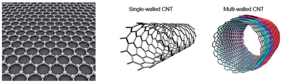
Carbon nanotubes composition, crystalline structure, fabrication and properties have been extensively reviewed over the years [6][7][8][9]. Briefly, carbon nanotubes are more easily described starting from graphene (Figure 1). Graphene consists of a single sheet of carbon atoms arranged in hexagonal cells with an in-plane structure. This form of coordination for carbon atoms is called the sp2 hybridization of carbon: the 2s orbital and two of the 2p orbitals (the px and py) hybridize to form 3 covalent (σ) bonds per carbon atom spread at 120 °C from each other (trigonal structure), while one electron in the pz orbital remains free to contribute to conduction. Carbon nanotubes (CNTs) can then be described as a rolled sheet of graphene with axial symmetry. They are sorted into two main categories, Single-Walled Carbon Nanotubes (SWCNTs) and Multi-Walled Carbon Nanotubes (MWCNTs) depending on the number of graphene layers rolled into a coaxial array (Figure 1). SWCNTs have typical diameters in the range 0.4 to 20 nm and typical lengths from 100 nm to 10 μm depending on the method used to synthesize them. In MWCNTs, each tube is separated from the next by 0.34 to 0.36 nm. MWCNTs may have diameter between 1 nm (double-walled carbon nanotubes (DWCNTs)) to 300 nm (about 100 coaxial tubes) and typical length from 1 μm to 150 μm. In both cases, the length-to-diameter ratio is very high, so they are regarded as 1D nanostructures. SWCNTs can be either semi-conducting or metallic depending on their chirality (the orientation of the lattice with respect to the tube axis) while MWCNT is metallic (except in rare DWCNTs cases).
2.2.2. Functionalization of CNTs
CNTs are very attractive as active materials in chemical sensors as they have high adsorption capability to a wide range of species. However, various results show the limited selectivity of pristine CNT-based chemical sensors (for both gas-phase and liquid-phase sensing): they are often sensitive to different analytes with the same range of magnitude of sensitivity and response time [12][13].
Functionalizing CNT consists in hybridizing them with other molecules either by covalent [14][15] or non-covalent bonds [16][17]. Functionalization is advantageous for selective sensing because the functionalizing molecules can be selected for their affinity to the target analyte. It has become the most popular approach to enhance the selectivity of CNT-based chemical sensors, though some studies report on modulating electrode material instead of functionalizing CNT as a mean to achieve selectivity [18].
One of the main challenges in using functionalization for selective sensing lies in ensuring that the changes occurring at the functionalizing molecules in the presence of the target analyte can be detected through the CNTs in the selected electronic device configuration. At the same time, the functionalization itself should not degrade dramatically the properties of the electronic device itself.
For instance, covalent functionalization is usually expected to allow for stronger charge transfer between CNT and functionalizing molecules, thus providing stronger sensitivity to the target analytes. However, covalent bonds degrade the crystalline structure of the CNTs, thus degrading their conduction properties and subsequently the transduction quality. As a consequence, the density of covalent functionalization that can be achieved in practice remains limited, which in turn may limit the gain in sensitivity and selectivity [19].
By contrast, using non-covalent functionalization, full coverage of the CNT surface may be achieved without degrading the intrinsic electronic properties of the CNTs; however, selecting functionalizing molecules that strongly impact the electronic properties of CNTs is challenging [20]. Usually, molecules that can functionalize CNTs by strong π-stacking are selected among aromatic molecules such as derivatives of benzene, fluorene, carbazole, or porphyrin, or conjugated polymers [21][22].
CNTs often carry some carboxyl groups (-COOH functions) on their sidewalls as a result of the synthesis process or of the post-synthesis purification (see Section 2.3.3). The density of these groups may for instance be evaluated by Raman spectroscopy [23][24], but is not systematically studied in the literature on CNT sensors. Hence CNTs reported on as non-functionalized CNTs may carry COOH groups. The COOH density may also be increased on purpose to enhance sensitivity to certain analytes, for instance by strong oxidative acidic treatments [25]. CNTs oxidized on purpose are labeled CNT-COOH. Articles reporting on those are classified jointly with the articles on pristine CNTs.
2.2.3. CNT-Based Electronic Devices
Using CNT in electrical sensors requires their integration into electronic devices. This topic has been extensively discussed in the literature (see reference [26] for instance). Briefly, one differentiates between devices based on as-grown CNTs or on prefabricated CNTs. Devices can be either based on a single CNT [27] or a CNT network [28]. In turn, this network may be either random or organized (for instance aligned).
In devices based on as-grown CNTs, CNTs are usually synthesized via chemical vapor deposition (CVD) directly onto pre-patterned electrodes within a temperature range from 550 °C to 1000 °C [29][30]. CVD CNT growth leads to robust electrode/CNT contacts and high CNT crystalline quality while avoiding bundling. However, the high-temperature CVD growth conditions usually prevent the use of flexible substrates. The need for metallic growth catalysts is often incompatible with the architecture of electronic devices (as they require well-defined insulating surfaces). For those reasons, as-grown CNT films are often transferred as a whole from the synthesis substrate onto more appropriate substrates via lift-off [29]. In addition, in-place synthesis does not allow for perfect control of CNT alignment, nor of their diameter, chirality or crystallinity, while these parameters have key impacts on device features. There are several purification and sorting techniques available to tune these parameters for CNTs on solid substrates. The most frequently reported post-growth processes are removal of the metallic CNTs by electrical breakdown [31] (application of a high current to a CNT network while the semiconducting CNTs are polarized in their OFF-state, which burns out metallic CNTs only) or degradation of the CNT crystalline quality by plasma etching [32], irradiation [33], or thermal oxidation [34].
By contrast, in devices relying on pre-fabricated CNTs, CNTs available in powder form are dispersed in a solvent and deposited onto the appropriate substrate via wet process. It is the most frequently reported approach to fabricate CNT-based sensors. It is advantageous because it features little constraints regarding substrates and because it allows the use of a large panel of solution-based CNT pre-treatment protocols, such as purification, acidification, functionalization, sorting by chirality or by diameter [35]. A large variety of techniques is available to deposit CNTs from a dispersion onto a substrate: drop-casting [36], spin coating [37], dip-coating [38], inkjet printing [39], spray-coating [40], aerosol jet printing [41] or vacumm filtering [42]. After substrate deposition of a CNT dispersion, particularly following drop casting, dielectrophoresis may then be used to improve on the deposition quality, notably to control accurately CNT positioning or to achieve CNT alignment [43]. After vaccum filtering, the filter may be removed, forming a freestanding film often called buckypaper [44]. Let us note that, despite the advantages of using prefabricated CNTs compared to in-place growth CNTs, it also has a few drawbacks, such as: CNT placement on the substrate may not be as accurate; low network density is more difficult to achieve; CNT-substrate interaction may be less strong; CNT crystallinity may be degraded during liquid phase processing steps such as high-power sonication.
2.3. CNT-Based Electrochemical Sensors
2.3.1. Electrochemical Cells
An electrochemical sensor is a device that detects an electron exchange between sensor and analyte. It is usually composed of two basic components, a chemical recognition layer and a physicochemical transducer, the latter comprising several metal electrodes, the working electrode, the reference electrode and in most cases a counter electrode. Immersed into an electrolyte solution, they make up the electrochemical cell (or voltaic or galvanic cell) [45].
A two-electrode cell consists of only working and reference electrodes. It is used for low current operation (small-sized working electrodes, very low analyte concentrations) because at higher current, the potential of the working electrode becomes unstable. In most applications, a three-electrode cell is used; the reference electrode is maintained at a stable potential, while the current passes through working and counter electrodes. Two types of process may occur in electrochemical cells. In a Faradaic process, charge particles transfer from electrode to electrode through the electrolyte. In non-Faradaic, charge is progressively stored [46].
2.3.2. Electrochemical Transduction
There are various types of electrochemical transducers depending on how the electrochemical cell is operated. The most popular ones are briefly described in the following paragraphs.
In potentiometric sensors, the measured signal is the potential difference between the working electrode and the reference electrode in the absence of current. The working electrode potential depends on the concentration of the target analyte. A reference electrode is needed to provide a defined reference potential. The response of a potentiometric sensor is interpreted using the Nernst equation, which states that the activity of the species of interest is in a logarithmic relationship with the potential difference [47]. This approach works well when the activity of a given species can be approximated to the molar concentration, namely at low concentration.
In voltammetric sensors, the current response is measured as a function of the applied potential. It is directly correlated to the rate of electron transfer occurring via electrochemical reactions [48]. This approach differentiates well species with different redox potential (separated by more than ±0.04–0.05 V). In turn, there are significant interfering effects if two or more species in the sample solution have similar redox potentials. There are different types of voltammetry depending on the way the voltage is applied, notably linear sweep or pulse-wise increase. The latter (usually called differential pulse voltammetry), is reported to be well suited for solid electrodes based on organic compound and more sensitive than the former (usually called cyclic voltammetry).
In electrochemical impedance spectroscopy (EIS), an alternating voltage is applied. The phase shift and amplitude of the current are measured over a range of frequencies. It provides information on the rate of the electrochemical reactions and on the ionic transport in the electrolyte [49].
Stripping voltammetry consists of two steps. First, target chemical species are electrolytically deposited on the surface of one of the electrodes using a constant potential, for instance by reduction of metal ions on the cathode. Second, a voltage scan is applied to the electrode, which progressively strips the target analytes from the electrode depending on their redox potential. At a given voltage, the resulting faradic current is proportional to the concentration of the target chemical ionic species [50]. If the different species are stripped at different voltages, selectivity is possible. The electrode deposition step has a pre-concentration effect on the target analyte, which yields this technique its considerable sensitivity (sub-nanomolar range for metal ions). Figure 2 shows example of measured responses by these three transduction methods.
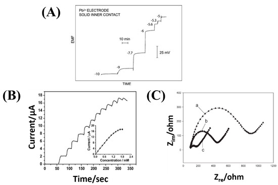
Figure 2. Measured response by three different transduction methods of electrochemical sensors: (A) Potentiometry (Potential at zero current—EMF electromotive force—vs. time under increasing volume of analyte—the numbers shown are logarithmic molar sample concentrations. Reproduced from [47] (B) Voltammetry (Current versus time under increasing volume of analyte) Reproduced from [51] (C) Electrochemical impedance spectroscopy (Nyquist plot: real impedance vs imaginary impedance for different of electrodes; a—Bare glassy carbon electrode (GCE) 1; b—CNTs/poly(1,2-diaminobenzene) prepared by cyclic voltammetry modified GCE; c—CNTs/poly(1,2-diaminobenzene) composite prepared by multipulse potentiostatic method modified GCE). Reproduced from [52].
2.3.3. Use of CNTs in Electrochemical Sensors
Because the performances of electrochemical sensors are driven by the specificities of the electrodes and of the electrolyte/electrode interfaces, improvements in sensor performances can be achieved by tuning either the electrode bulk material or the electrode surfaces, the latter using either dedicated coatings or by surface engineering (for instance, roughness increase). CNTs are used both as coatings and as electrode material to leverage their high specific surface area. It allows for a large dynamic range and for a high loading in electrocatalysts (defined as the catalysts that participate in electrochemical reactions by increasing the rate of chemical reactions without being consumed in the process). Moreover, CNTs display resistance to fouling [53].
The details of the composition and fabrication process of the various CNT-based electrochemical sensors reported are provided later. As a summary, out of 66 reports, 31 (47%) reports address CNTs coated on glassy carbon electrodes, 10 (15%) are about electrodes directly made out of CNTs or CNT paste, the rest electrodes being made of miscellaneous metallic materials (gold, steel …). The most used method for coating electrodes with CNTs is drop casting (28 references, 42%): CNTs are first purified, then chemically activated (either oxidized or functionalized) and dispersed in a solvent with sonication. The dispersion is then dropped on the electrode surfaces and the solvent is evaporated rapidly [51][54][55][56][57][58][59].
The prevalence of drop-casting methods is due to their simple implementation. They are often used as a stepping stone on the path toward more reproducible, but often less straightforward, fabrication processes. One of the main shortcomings of techniques based on CNT dispersion (drop and spray casting, dip coating, dielectrophoresis, printing …) is that most solvents have low exfoliation efficiency for CNTs and the resulting solutions have low stability due to the rather weak interactions between these solvents and CNTs [60]. As a consequence, CNT-paste-based electrodes are a popular alternative to CNT-coated electrodes (13 references, 20%). The reported binders are often mineral oils, often mixed with graphite powder and/or ionic liquids ([61][62]).
Regarding electrochemical sensing mechanisms, the carbon atoms at the CNT ends have been shown to behave like the edge planes of highly orientated pyrolytic graphite (HOPG) and to feature rapid electron transfer kinetics: they contribute to the Faradaic processes and provide quick response time. By contrast, the carbon atoms of the sidewalls resemble the basal plane of HOPG and show slower electron transfer kinetics than end atoms [63] (though still higher than HOPG due to curvature [64]). In other words, they are much less involved in oxidoreduction reactions with the electrolyte. However, they contribute to non-Faradaic processes driven by adsorption and desorption mechanisms.
The processes enabling removal of the impurities from CNTs that remain from the synthesis process (carbon nanoparticles, nanocrystal metal catalysts, amorphous carbon …) play a strong role in the electrochemical properties of the CNTs. Raw CNTs are usually purified before use by thermal treatment at around 400 °C or by chemical oxidation via acidic treatment. It leads to shortened and partially oxidized CNT. In particular, the resulting CNTs feature functional oxygenated groups at the open ends and an increased defect density along the sidewalls [65]. In addition to CNT curvature, those defects also explain that CNT sidewalls contribute to the Faradaic process in electrochemical sensors. Luo et al. for instance detailed the oxidation–reduction reactions for carboxylic CNT sidewall defects in [66].
2.4. CNT-Based Chemistors
2.4.1. Chemistors
Chemi-resistors, or chemistors, are sensors operating by measuring the variation in the electrical resistance or the resistivity of a sensing (also called active) material as a consequence of its interaction with the target analyte. The target analyte has to be in direct contact or close proximity to the active material. The possible interactions are highly diversified: bulk or catalytic reactions, reversible or irreversible, chemi- or physisorption, surface or volume reactions or reactions at grain boundaries [67].
In most chemistors, resistance changes are measured in a two-terminal configuration (Figure 3a,b). A small constant current is applied between two electrodes separated by a short distance (µm to mm) and the resulting voltage is measured. Alternately, four-terminal configurations may also be used to reduce the influence of contact resistance on the sensitivity, especially in the case of high resistance devices (MΩ range and higher). Four parallel electrodes are often used in those cases; the current is applied on the external electrodes and the voltage drop is measured across the two internal electrodes. In the case of arbitrary electrode disposition (for instance, anisotropic surface), the Van der Pauw method can be used to measure the bulk resistivity (ρ) and the Hall coefficient of the surface by using four different contact point [68].
2.4.2. Use of CNT in Chemistors
The use of CNT as active layer and/or electrode material in chemistor is prominent across various sensing applications (gas sensing, biological sensing) [69], as it is the most straightforward device structure available to assess sensitivity of CNTs to chemicals (in terms of design, fabrication, electronics, signal processing …). The high surface area results in high adsorption rates for analytes leading to a rapid response time. Typically, only a fraction of µg or less of CNT material is needed, so the raw material cost is not a limiting factor [70]. Moreover, a small (1 cm2) chip-based device can hold hundreds of sensor elements. Such miniaturization leads to a reduction in size and weight of the assembled systems.
Most reports on chemistors (10 out of 13) use SWCNTs rather than MWCNTs. CNT chemistors are mostly often fabricated using electrode materials made of noble metals (platinum and gold), though occasionally (here 4 reports out of 12) the CNTs make up both electrode material and active layer. The electrode metal is usually thermally evaporated on the substrate and patterned with photolithography. After purification (eliminating synthesis residues), sorting (for instance by diameter) and dispersion in a solvent, the CNTs are deposited across the gap, bridging the electrodes or electrode fingers (Figure 3a,b), then the solvent is evaporated. Various methods can be used for this deposition step, either wet-processing techniques (such as drop-casting, inkjet printing, spraying …—11 references) or dry-processing techniques (such as direct (in-place) chemical vapor deposition (CVD) growth or CVD-growth followed by solid-state transfer or by nanoimprint as nano-scale patterning process—2 references). The CNT networks are in most cases random (except in 3 references where there are aligned through dielectrophoresis [71] or threading of CVD-aligned CNTs [72]).
The baseline resistance level of a device and its sensitivity depends on the geometry of the electrodes, on the type and quality of CNTs as well as on their surface density. The latter actually depends on both the CNT concentration in the dispersion and the selected deposition process. The geometry of the electrodes is characterized primarily by their spacing—often called the gap—and the length of the gap. The gap ranges between 1 µm and 100 µm, with the gap length of between 10 µm and several mm. To optimize space occupation, the electrodes are often interdigitated (Figure 3c): instead of a straight gap, the gap is formed by a series of parallel fingers. The effective gap length is thus roughly equal to twice the finger length multiplied by the number of fingers. Finger widths are typically in the 1 to 10 µm range, lengths in the 10 to 100 µm range [73][74].
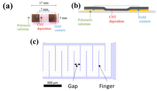
Figure 3. (a) Top view and (b) cross section of an example of two terminal resistive CNT sensors on ETFE (Ethylene Tetra Fluoro Ethylene). Reproduced from [75]. (c) Schematic of interdigitated electrodes.
2.5. CNT-Based ChemFET
2.5.1. ChemFET
A field-effect transistor (FET) is an electronic device consisting of a semiconducting layer, called channel, located between a source and a drain electrode; the density of electronic carriers flowing in the channel between source and drain electrodes is modulated by the potential of a third electrode, called gate electrode, close to the channel and insulated from it by a dielectric material. A chemical FET—chemFET—is a FET whose conduction characteristics are modulated by the presence and concentration of analytes around the device. The chemically sensitive layer is usually the semiconducting channel, though the electrodes and the dielectric layer have been reported to contribute to sensitivity. The device design allows for the semiconducting layer to be exposed to the target liquid. In an electrolyte-gated chemFET, the target liquid itself is used as both the gate and dielectric layer.
In broad terms, chemFETs are similar to chemistors in the sense that they can be described as chemistors whose baseline resistance is controlled by the gate voltage. Similarly to chemistors, chemical detection is enabled by short-range interactions between the target analyte and the active layer. However, while in chemistors only the resistance (and sometimes the resistivity and contact resistance) of the active layer may be exploited to derive the analyte concentration, there are much more varying parameters in chemFET architectures, which offers a finer understanding of the sensing mechanisms.
In more details, the electrical properties of chemFETs are derived from measuring its drain-source current Ids as a function of gate Vg and drain voltage Vd. From these curves are extracted synthetic parameters such as: (i) in the linear regime of Ids as a function of Vd, the (gate-voltage controlled chemFET resistance (slope of Ids(Vd)); (ii) the ratio between ON and OFF current levels (values of Ids when the semiconducting channel is respectively in its most conducting—ON—and most insulating—OFF—state); (iii) the transconductance (the maximum value of the first derivative of Ids(Vg), which is related to the mobility of the semiconducting channel); (iv) the threshold voltage (gate voltage value for which the semiconducting channel transitions from insulating to conducting); (v) the hysteresis observed between threshold voltage values or transconductance values during upward and downward sweep of the gate voltage [76][77][78]. Regarding the latter, this hysteresis is attributed in large part to the adsorption of water molecules on the device surface creating charging effect [79]. Hence, it is expected to be a particularly relevant indicator in CNTFET-based water quality sensors but there has very been little study on it so far [80]. Because of this diversity of output parameters, chemFETs are usually considered to be more sensitive and more selective than chemistors. In turn, they usually require significantly more complex fabrication and characterization procedures as well as operating electronics and signal processing.
2.5.2. Use of CNT in ChemFET
CNT-FET is a chemFET with a CNT layer as channel. Because a semiconducting channel is required, only single-walled carbon nanotubes (SWCNTs) can be used [81] (MWCNTs being metallic). In general, the CNT-FET channel may be formed either by a single semi-conducting SWCNT or by a percolating network of SWCNTs with a semi-conducting behavior [82]. While devices based on a single SWCNT have remarkable electrical performances [26][83], devices based on a random-network of SWCNTs are more popular for sensing applications due to their higher effective sensing area, their simpler fabrication procedure as well as their better up-scalability (for mass production), even though their electrical performances are not as good as these of single SWCNT devices. In the field of water quality monitoring, only devices based on networks of CNT have been reported so far. Those networks are in most cases random except in 2 references where CNTs are aligned through dielectrophoresis [43][84].
As SWCNTs may be either semi-conducting or metallic depending on their chiral structure, percolating networks of SWCNTs are not normally semi-conducting because they contain a significant ratio of metallic SWCNTs. To achieve semiconducting SWCNTs networks, a variety of processes is available. For instance, semiconducting SWCNT may be sorted before deposition; electrical breakdown of metallic SWCNTs after their deposition or their in-place growth can also be used; almost systematically, low density networks are used to minimize the chance of forming a metallic path between electrodes [85][86][87].
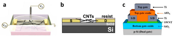
There are four main types of device architecture for CNT-FET chemical sensors: top gate, bottom gate, liquid gate and hybrid structures; Among 11 reported CNT-FET-based chemical sensors, two are top-gated [88][89], three bottom-gated [90][91][92] and five liquid gated [43][93][94][95][96]. Finally, one is a hybrid dual-gate structure [37] (Figure 4). The original architecture is the bottom gate one, where the gate is embedded below the semiconducting layer with a separating dielectric layer [90]. In the context of water quality monitoring, it has the significant drawback of requiring a high gate voltage (usually several tens of Volts) for good electrical performances, which leads to hydrolysis of water (beyond 1 V). In top gate structures, the gate layer is located on top of the semiconducting channel instead, which makes it more straightforward to fabricate. It requires a lower operating gate voltage, but it is relatively little used for sensing applications as well because the top gate insulates the sensitive channel from the environment. A variation on the top gate structure, the liquid gate structure, consists in applying the gate voltage through the electrolyte surrounding the device [97]. It is particularly interesting for chemical sensing in water because it allows much lower-voltage operation (in the sub-volt range) compared to the usual bottom-gate structure (Figure 4a) [98]. It is also more straightforward to fabricate considering that it requires one less electrode by an embedded gate structure compared to the top gate structure [95]. Hybrid CNT-FET architectures consist in coupling in the same architecture several gating strategies. Notably, Pyo et al. [37] fabricated a double-gated CNT-FET with a separated extended gate. The extended gate concept consists on placing an ion-sensitive membrane on top of the top gate of the double-gated CNT-FET (Figure 4c).
SiO2 is the most frequently used dielectric material used for the layer between the semiconducting channel and the substrate or gate electrode (Figure 4b) (6 papers out of 11). However, oxides with a higher dielectric constant such as Al2O3 or Si3N4 may also be used in order to have a thinner insulating layer with better homogeneity and durability compared to SiO2 [99]. Takeda et al. used a sol-gel layer of 3-aminopropyltriethoxysilane (APS) as insulating layer, with the goal to better immobilize the SWCNTs in water [89]. Indeed, an electrostatic attraction occurs between the negatively-charged carboxyl groups of SWCNTs and the positively-charged APS.
2.6. Sensing Mechanisms in CNT-Based Chemistors and ChemFET
The mechanisms of sensitivity of CNT-based chemistors and chemFET are usually extrapolated from their mechanisms of sensitivity to gas [100], mechanisms that still remain somewhat debated. Overall, the response to analytes is attributed to a change in the conduction properties of either, or all, of the three following components of the devices, as shown in Figure 5 [101]: The conduction along the tube length (“intra-CNT”), the contact points between tubes behaving as tunnel junctions (“inter-CNT”) and the contact points between the tubes and the metal electrodes behaving as Schottky barriers. Sensitivity is attributed either to direct adsorption of the analytes on these sites, or to analytes not adsorbed, but at a distance small enough to these sites to perturb their electrical behavior.
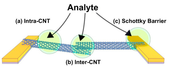
Figure 5. Schematic of possible sensitivity sites which affect the conductivity: (a) at the sidewall or along the length of the CNT itself, (b) interface between CNT-CNT (inter-CNT) and (c) at the interface between the metal electrodes and the CNT (Schottky barrier). Reprinted with permission from [101]. Copyright (2018) from American Chemical Society.
Modulation of the Schottky barrier is caused by a change in the work function of either the electrode metal or the CNTs in presence of the target analytes. The inter-CNT modulation corresponds to a change in the transmission coefficient of the inter-tube tunneling junction, which in turn can be attributed to either a change in the inter-tube distance, or a change in the work functions of the tubes. The intra-CNT conduction modulation is caused by a change either in the density of charge along the sidewalls (resulting in a doping effect) or in the carrier scattering properties of the sidewalls (impacting mobility).
Each of these three modulations may impact the global device response, with specificities depending on the type of transduction (ChemET or chemistor) and on the device morphology (particularly on the network density).
Regarding ChemFETs, Figure 6 provides an insight into the impact of the Schottky-barrier modulation and the intra-CNT modulation (doping or mobility variation) on the typical I-V characteristics of a chemFET [101]. Inter-CNT effects (contact resistance modulation) are usually neglected when analyzing sensing performances of chemFET as their electric performances are mostly driven by intra-CNT effects and Schottky barrier modulation.
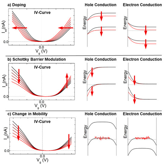
Figure 6. Theoretical I-V curves of a chemFET depending on (a) the doping (b) Scottky barrier modulation (c) change in mobility. Reprinted with permission from [101]. Copyright (2018) from American Chemical Society.
By contrast, in chemistors, the inter-CNT modulation is generally accepted to have the strongest impact on the device response, as the global baseline resistance of the network is mostly controlled by inter-CNT contacts. This is confirmed by modeling results for high density networks. In low density networks, modeling suggests that the variations of the electrode-CNT resistance and of the intra-CNT resistance may also contribute to the global relative resistance variation occurring upon exposure to chemicals [102].
References
- Hinrichsen, D.; Tacio, H. The Coming Freshwater Crisis Is Already Here; ESCP Publication: Washington, DC, USA, 2002; pp. 1–26.
- Solomon, A.; Ahmed, Z.; Biruktawit, K.; Amare, D.; Solomon, A.; Endalew, Z.; Abera, S.; Zeyinudin, A.; Kebede, B.; Deribew, A.; et al. Bacteriological analysis of drinking water sources. Afr. J. Microbiol. Res. 2011, 5, 2638–2641.
- Aydin, A. The microbiological and physico-chemical quality of groundwater in West Thrace, Turkey. Pol. J. Environ. Stud. 2007, 16, 377–383.
- Gyamfi, E.; Ackah, M.; Anim, A.; Hanson, J.; Kpattah, L.; Enti-Brown, S.; Adjei-Kyereme, Y.; Nyarko, E. Chemical analysis of potable water samples from selected suburbs of Accra, Ghana. Proc. Int. Acad. Ecol. Environ. Sci. 2012, 2, 118–127.
- Vikesland, P.J.; Wigginton, K.R. Nanomaterial Enabled Biosensors for Pathogen Monitoring—A Review. Environ. Sci. Technol. 2010, 44, 3656–3669.
- Iijima, S.; Ichihashi, T. Single-shell carbon nanotubes of 1-nm diameter. Nature 1993, 363, 603–605.
- Belin, T.; Epron, F. Characterization methods of carbon nanotubes: A review. Mater. Sci. Eng. B 2005, 119, 105–118.
- Qiu, H.; Yang, J. Chapter 2—Structure and Properties of Carbon Nanotubes. In Industrial Applications of Carbon Nanotubes; Peng, H., Li, Q., Chen, T., Eds.; Elsevier: Boston, MA, USA, 2017; pp. 47–69.
- Soni, S.K.; Thomas, B.; Kar, V.R. A Comprehensive Review on CNTs and CNT-Reinforced Composites: Syntheses, Characteristics and Applications. Mater. Today Commun. 2020, 25, 101546.
- Aius, A. Graphene Honeycomb Lattice. CC BY-SA 3.0.
- Zhang, Y.; Bai, Y.; Yan, B. Functionalized carbon nanotubes for potential medicinal applications. Drug Discov. Today 2010, 15, 428–435.
- Zhang, T.; Mubeen, S.; Myung, N.V.; Deshusses, M.A. Recent progress in carbon nanotube-based gas sensors. Nanotechnology 2008, 19, 332001.
- Andringa, A.-M.; Meijboom, J.R.; Smits, E.C.P.; Mathijssen, S.G.J.; Blom, P.W.M.; de Leeuw, D.M. Gate-Bias Controlled Charge Trapping as a Mechanism for NO2 Detection with Field-Effect Transistors. Adv. Funct. Mater. 2010, 21, 100–107.
- Hirsch, A. Functionalization of single-walled carbon nanotubes. Angew. Chem. Int. Ed. 2002, 41, 1853–1859.
- Banerjee, S.; Hemraj-Benny, T.; Wong, S.S. Covalent Surface Chemistry of Single-Walled Carbon Nanotubes. Adv. Mater. 2005, 17, 17–29.
- Star, A.; Stoddart, J.F.; Steuerman, D.; Diehl, M.; Boukai, A.; Wong, E.W.; Yang, X.; Chung, S.-W.; Choi, H.; Heath, J.R. Preparation and Properties of Polymer-Wrapped Single-Walled Carbon Nanotubes. Angew. Chem. Int. Ed. 2001, 40, 1721–1725.
- Britz, D.A.; Khlobystov, A.N. Noncovalent interactions of molecules with single walled carbon nanotubes. Chem. Soc. Rev. 2006, 35, 637–659.
- Bondavalli, P.; Gorintin, L.; Feugnet, G.; Lehoucq, G.; Pribat, D. Selective gas detection using CNTFET arrays fabricated using air-brush technique, with different metal as electrodes. Sens. Actuators B Chem. 2014, 202, 1290–1297.
- Cardenas-Benitez, B.; Djordjevic, I.; Hosseini, S.; Madou, M.J.; Martinez-Chapa, S.O. Review—Covalent Functionalization of Carbon Nanomaterials for Biosensor Applications: An Update. J. Electrochem. Soc. 2018, 165, B103–B117.
- Zhou, Y.; Fang, Y.; Ramasamy, R.P. Non-Covalent Functionalization of Carbon Nanotubes for Electrochemical Biosensor Development. Sensors 2019, 19, 392.
- Toshimitsu, F.; Nakashima, N. Semiconducting single-walled carbon nanotubes sorting with a removable solubilizer based on dynamic supramolecular coordination chemistry. Nat. Commun. 2014, 5, 5041.
- Zucchi, G.; Lebental, B.; Loisel, L.; Ramachandran, S.; Gutiérrez, A.F.; Wang, X.; Godumala, M.; Bodeleot, L. Chemical Sensors Based on Carbon Nanotubes Functionalised by Conjugated Polymers for Analysis in Aqueous Medium. Patent 3609881A1, 10 April 2018.
- Gómez, S.; Rendtorff, N.M.; Aglietti, E.F.; Sakka, Y.; Suárez, G. Surface modification of multiwall carbon nanotubes by sulfonitric treatment. Appl. Surf. Sci. 2016, 379, 264–269.
- Gong, H.; Kim, S.-T.; Lee, J.D.; Yim, S. Simple quantification of surface carboxylic acids on chemically oxidized multi-walled carbon nanotubes. Appl. Surf. Sci. 2013, 266, 219–224.
- Wepasnick, K.A.; Smith, B.A.; Schrote, K.E.; Wilson, H.K.; Diegelmann, S.R.; Fairbrother, D.H. Surface and structural characterization of multi-walled carbon nanotubes following different oxidative treatments. Carbon 2011, 49, 24–36.
- Anantram, M.P.; Léonard, F. Physics of carbon nanotube electronic devices. Rep. Prog. Phys. 2006, 69, 507–561.
- Tans, S.J.; Verschueren, A.R.M.; Dekker, C. Room-temperature transistor based on a single carbon nanotube. Nature 1998, 393, 49–52.
- Snow, E.S.; Novak, J.P.; Campbell, P.M.; Park, D. Random networks of carbon nanotubes as an electronic material. Appl. Phys. Lett. 2003, 82, 2145–2147.
- Zhou, X.; Boey, F.; Zhang, H. Controlled growth of single-walled carbon nanotubes on patterned substrates. Chem. Soc. Rev. 2011, 40, 5221–5231.
- Ahmad, M.; Silva, S.R.P. Low temperature growth of carbon nanotubes—A review. Carbon 2020, 158, 24–44.
- Seidel, R.; Graham, A.P.; Unger, E.; Duesberg, G.S.; Liebau, M.; Steinhoegl, W.; Kreupl, F.; Hoenlein, W.; Pompe, W. High-Current Nanotube Transistors. Nano Lett. 2004, 4, 831–834.
- Zhang, G.; Qi, P.; Wang, X.; Lu, Y.; Li, X.; Tu, R.; Bangsaruntip, S.; Mann, D.; Zhang, L.; Dai, H. Selective Etching of Metallic Carbon Nanotubes by Gas-Phase Reaction. Science 2006, 314, 974–977.
- Zhang, Y.; Zhang, Y.; Xian, X.; Zhang, J.; Liu, Z. Sorting out Semiconducting Single-Walled Carbon Nanotube Arrays by Preferential Destruction of Metallic Tubes Using Xenon-Lamp Irradiation. J. Phys. Chem. C 2008, 112, 3849–3856.
- Zhao, Q.; Yao, F.; Wang, Z.; Deng, S.; Tong, L.; Liu, K.; Zhang, J. Real-Time Observation of Carbon Nanotube Etching Process Using Polarized Optical Microscope. Adv. Mater. 2017, 29, 1701959.
- Lei, T.; Pochorovski, I.; Bao, Z. Separation of Semiconducting Carbon Nanotubes for Flexible and Stretchable Electronics Using Polymer Removable Method. Acc. Chem. Res. 2017, 50, 1096–1104.
- Hsu, L.H.H.; Hoque, E.; Kruse, P.; Selvaganapathy, P.R. A carbon nanotube based resettable sensor for measuring free chlorine in drinking water. Appl. Phys. Lett. 2015, 106, 063102.
- Pyo, J.-Y.; Cho, W.-J. High-sensitivity pH sensor using separative extended-gate field-effect transistors with single-walled carbon-nanotube networks. Jpn. J. Appl. Phys. 2018, 57, 04FP02.
- Wei, L.; Lu, D.; Wang, J.; Wei, H.; Zhao, J.; Geng, H.; Zhang, Y. Highly sensitive detection of trinitrotoluene in water by chemiresistive sensor based on noncovalently amino functionalized single-walled carbon nanotube. Sens. Actuators B Chem. 2013, 190, 529–534.
- Eshkalak, S.K.; Chinnappan, A.; Jayathilaka, D.; Khatibzadeh, M.; Kowsari, E.; Ramakrishna, S. A review on inkjet printing of CNT composites for smart applications. Appl. Mater. Today 2017, 9, 372–386.
- Kwon, J.-H.; Lee, K.-S.; Lee, Y.-H.; Ju, B.-K. Single-Wall Carbon Nanotube-Based pH Sensor Fabricated by the Spray Method. Electrochem. Solid-State Lett. 2006, 9, H85–H87.
- Goh, G.L.; Agarwala, S.; Tan, Y.J.; Yeong, W.Y. A low cost and flexible carbon nanotube pH sensor fabricated using aerosol jet technology for live cell applications. Sens. Actuators B Chem. 2018, 260, 227–235.
- Stojanović, G.; Kojić, T.; Radovanović, M.; Vasiljević, D.; Panić, S.; Srdić, V.; Cvejić, J. Flexible sensors based on two conductive electrodes and MWCNTs coating for efficient pH value measurement. J. Alloys Compd. 2019, 794, 76–83.
- Gou, P.; Kraut, N.D.; Feigel, I.M.; Bai, H.; Morgan, G.J.; Chen, Y.; Tang, Y.; Bocan, K.; Stachel, J.; Berger, L.; et al. Carbon Nanotube Chemiresistor for Wireless pH Sensing. Sci. Rep. 2014, 4, 4468.
- Endo, M.; Muramatsu, H.; Hayashi, T.; Kim, Y.A.; Terrones, M.; Dresselhaus, M.S. ‘Buckypaper’ from coaxial nanotubes. Nature 2005, 433, 476.
- Bard, A.J.; Faulkner, R.L. Electrochemical Methods: Fundamentals and Applications, 2nd ed.; Wiley: Hoboken, NJ, USA, 2001; Volume 38, pp. 1364–1365.
- Biesheuvel, P.M.; Porada, S.; Dykstra, J.E. The difference between Faradaic and non-Faradaic electrode processes. arXiv 2021, arXiv:1809.02930.
- Bakker, E.; Pretsch, E. Potentiometric sensors for trace-level analysis. TrAC Trends Anal. Chem. 2005, 24, 199–207.
- Hanrahan, G.; Patil, D.G.; Wang, J. Electrochemical sensors for environmental monitoring: Design, development and applications. J. Environ. Monit. 2004, 6, 657–664.
- Simões, F.R.; Xavier, M.G. 6—Electrochemical Sensors. In Nanoscience and Its Applications; Róz, A.L.D., Ferreira, M., Leite, F.L., Osvaldo, N., Oliveira, A., Eds.; William Andrew Publishing: Norwich, NY, USA, 2017; pp. 155–178.
- March, G.; Nguyen, T.D.; Piro, B. Modified Electrodes Used for Electrochemical Detection of Metal Ions in Environmental Analysis. Biosensors 2015, 5, 241–275.
- Zhou, H.; Yang, W.; Sun, C. Amperometric sulfite sensor based on multiwalled carbon nanotubes/ferrocene-branched chitosan composites. Talanta 2008, 77, 366–371.
- Gao, X.; Wei, W.; Yang, L.; Guo, M. Carbon Nanotubes/Poly(1,2-diaminobenzene) Nanoporous Composite Film Electrode Prepared by Multipulse Potentiostatic Electropolymerisation and Its Application to Determination of Trace Heavy Metal Ions. Electroanalysis 2006, 18, 485–492.
- Farid, M.U.; Khanzada, N.K.; An, A.K. Understanding fouling dynamics on functionalized CNT-based membranes: Mechanisms and reversibility. Desalination 2019, 456, 74–84.
- Britto, P.; Santhanam, K.; Ajayan, P. Carbon nanotube electrode for oxidation of dopamine. Bioelectrochem. Bioenerg. 1996, 41, 121–125.
- Xu, H.; Zeng, L.; Xing, S.; Shi, G.; Xian, Y.; Jin, L. Microwave-radiated synthesis of gold nanoparticles/carbon nanotubes composites and its application to voltammetric detection of trace mercury(II). Electrochem. Commun. 2008, 10, 1839–1843.
- Xu, H.; Zeng, L.; Xing, S.; Xian, Y.; Shi, G.; Jin, L. Ultrasensitive Voltammetric Detection of Trace Lead(II) and Cadmium(II) Using MWCNTs-Nafion/Bismuth Composite Electrodes. Electroanalysis 2008, 20, 2655–2662.
- Morton, J.; Havens, N.; Mugweru, A.; Wanekaya, A.K. Detection of Trace Heavy Metal Ions Using Carbon Nanotube- Modified Electrodes. Electroanalysis 2009, 21, 1597–1603.
- Zhang, W.; Wang, G.; Zhang, X.; Fang, B. Amperometric Detection of Hydrogen Peroxide Using Glassy Carbon Electrodes Modified with Chromium Hexacyanoferrate/Single-Walled Carbon Nanotube Nanocomposites. Electroanalysis 2009, 21, 179–183.
- Hu, F.; Chen, S.; Wang, C.; Yuan, R.; Yuan, D.; Wang, C. Study on the application of reduced graphene oxide and multiwall carbon nanotubes hybrid materials for simultaneous determination of catechol, hydroquinone, p-cresol and nitrite. Anal. Chim. Acta 2012, 724, 40–46.
- Hu, C.; Hu, S. Carbon Nanotube-Based Electrochemical Sensors: Principles and Applications in Biomedical Systems. J. Sens. 2009, 2009, 187615.
- Karimi-Maleh, H.; Ensafi, A.A.; Beitollahi, H.; Nasiri, V.; Khalilzadeh, M.A.; Biparva, P. Electrocatalytic determination of sulfite using a modified carbon nanotubes paste electrode: Application for determination of sulfite in real samples. Ionics 2012, 18, 687–694.
- Khani, H.; Rofouei, M.K.; Arab, P.; Gupta, V.K.; Vafaei, Z. Multi-walled carbon nanotubes-ionic liquid-carbon paste electrode as a super selectivity sensor: Application to potentiometric monitoring of mercury ion(II). J. Hazard. Mater. 2010, 183, 402–409.
- Gong, K.; Yan, Y.; Zhang, M.; Su, L.; Xiong, S.; Mao, L. Electrochemistry and Electroanalytical Applications of Carbon Nanotubes: A Review. Anal. Sci. 2005, 21, 1383–1393.
- He, Y.; Chen, W.; Gao, C.; Zhou, J.; Li, X.; Xie, E. An overview of carbon materials for flexible electrochemical capacitors. Nanoscale 2013, 5, 8799–8820.
- Zhang, J.; Zou, H.; Qing, Q.; Yang, Y.; Li, Q.; Liu, Z.; Guo, A.X.; Du, Z. Effect of Chemical Oxidation on the Structure of Single-Walled Carbon Nanotubes. J. Phys. Chem. B 2003, 107, 3712–3718.
- Luo, H.; Shi, Z.; Li, N.; Gu, Z.; Zhuang, Q. Investigation of the Electrochemical and Electrocatalytic Behavior of Single-Wall Carbon Nanotube Film on a Glassy Carbon Electrode. Anal. Chem. 2001, 73, 915–920.
- Zahab, A.; Spina, L.; Poncharal, P.; Marlière, C. Water-vapor effect on the electrical conductivity of a single-walled carbon nanotube mat. Phys. Rev. B 2000, 62, 10000–10003.
- Van der Pauw, L.J. A method of measuring specific resistivity and hall effect of discs of arbitrary shape. Philips Res. Rep. 1958, 13, 1–9.
- Tang, R.; Shi, Y.; Hou, Z.; Wei, L. Carbon nanotube-based chemiresistive sensors. Sensors 2017, 17, 882.
- Meyyappan, M. Carbon Nanotube-Based Chemical Sensors. Small 2016, 12, 2118–2129.
- Li, P.; Martin, C.M.; Yeung, K.K.; Xue, W. Dielectrophoresis aligned single-walled carbon nanotubes as pH sensors. Biosensors 2011, 1, 23–35.
- Jung, D.; Han, M.; Lee, G.S. pH-sensing characteristics of multi-walled carbon nanotube sheet. Mater. Lett. 2014, 122, 281–284.
- Li, J.; Lu, Y.; Ye, Q.; Delzeit, L.; Meyyappan, M. A Gas Sensor Array Using Carbon Nanotubes and Microfabrication Technology. Electrochem. Solid-State Lett. 2005, 8, H100–H102.
- Li, J.; Lu, Y.; Ye, Q.; Cinke, M.; Han, J.; Meyyappan, M. Carbon Nanotube Sensors for Gas and Organic Vapor Detection. Nano Lett. 2003, 3, 929–933.
- Michelis, F.; Bodelot, L.; Bonnassieux, Y.; Lebental, B. Highly reproducible, hysteresis-free, flexible strain sensors by inkjet printing of carbon nanotubes. Carbon 2015, 95, 1020–1026.
- Naderi, A.; Tahne, B.A. Review—Methods in Improving the Performance of Carbon Nanotube Field Effect Transistors. ECS J. Solid State Sci. Technol. 2016, 5, M131–M140.
- Imam, S.-A.; Kalam, N.; Abdullah, S. Comparative Analysis of Control Coefficients on the Performance of CNTFET Under Different Parameters. Int. J. Nanosci. 2016, 15, 1640005.
- Karimi, N.V.; Pourasad, Y. Investigating the effect of some parameters of the channel on the characteristics of tunneling carbon nanotube field-effect transistor. Int. Nano Lett. 2016, 6, 215–221.
- Kim, W.; Javey, A.; Vermesh, O.; Wang, Q.; Li, A.Y.; Dai, H. Hysteresis Caused by Water Molecules in Carbon Nanotube Field-Effect Transistors. Nano Lett. 2003, 3, 193–198.
- Joshi, S.; Bhatt, V.D.; Rani, H.; Becherer, M.; Lugli, P. Understanding the influence of in-plane gate electrode design on electrolyte gated transistor. Microelectron. Eng. 2018, 199, 87–91.
- Saito, R.; Fujita, M.; Dresselhaus, G.; Dresselhaus, M.S. Electronic structure of chiral graphene tubules. Appl. Phys. Lett. 1992, 60, 2204–2206.
- Di Bartolomeo, A.; Rinzan, M.; Boyd, A.K.; Yang, Y.; Guadagno, L.; Giubileo, F.; Barbara, P. Electrical properties and memory effects of field-effect transistors from networks of single- and double-walled carbon nanotubes. Nanotechnology 2010, 21, 115204.
- Derycke, V.; Martel, R.; Appenzeller, J.; Avouris, P. Carbon Nanotube Inter- and Intramolecular Logic Gates. Nano Lett. 2001, 1, 453–456.
- Zhao, J.; Hashmi, A.; Xu, J.; Xue, W. A compact lab-on-a-chip nanosensor for glycerol detection. Appl. Phys. Lett. 2012, 100, 243109.
- Pimparkar, N.; Kocabas, C.; Kang, S.J.; Rogers, J.; Alam, M. Limits of Performance Gain of Aligned CNT Over Randomized Network: Theoretical Predictions and Experimental Validation. IEEE Electron Device Lett. 2007, 28, 593–595.
- Barman, S.N.; Lemieux, M.C.; Baek, J.; Rivera, R.; Bao, Z. Effects of Dispersion Conditions of Single-Walled Carbon Nanotubes on the Electrical Characteristics of Thin Film Network Transistors. ACS Appl. Mater. Interfaces 2010, 2, 2672–2678.
- Ruiz-Soria, G.; Paz, A.P.; Sauer, M.; Mowbray, D.J.; Lacovig, P.; Dalmiglio, M.; Lizzit, S.; Yanagi, K.; Rubio, A.; Goldoni, A.; et al. Revealing the adsorption mechanisms of nitroxides on ultrapure, metallicity-sorted carbon nanotubes. ACS Nano 2014, 8, 1375–1383.
- Park, M.; Kim, H.S.; Kim, T.; Kim, J.; Seo, S.; Lee, B.Y. Real-time monitoring of microbial activity using hydrogel-hybridized carbon nanotube transistors. Sens. Actuators B Chem. 2018, 263, 486–492.
- Takeda, S.; Nakamura, M.; Ishii, A.; Subagyo, A.; Hosoi, H.; Sueoka, K.; Mukasa, K. A pH sensor based on electric properties of nanotubes on a glass substrate. Nanoscale Res. Lett. 2007, 2, 207–212.
- Münzer, A.; Melzer, K.; Heimgreiter, M.; Scarpa, G. Random CNT network and regioregular poly(3-hexylthiophen) FETs for pH sensing applications: A comparison. Biochim. Biophys. Acta (BBA)-Gen. Subj. 2013, 1830, 4353–4358.
- Chernov, A.I.; Eremina, V.A.; Shook, J.; Collins, A.; Walker, P.; Fedotov, P.V.; Zakhidov, A.A.; Obraztsova, E.D. Field Effect Transistor Based on Solely Semiconducting Single-Walled Carbon Nanotubes for the Detection of 2-Chlorophenol. Phys. Status Solidi B 2017, 255, 1700139.
- Lee, N.H.; Nahm, S.-H.; Choi, I.S. Real-Time Monitoring of a Botulinum Neurotoxin Using All-Carbon Nanotube-Based Field-Effect Transistor Devices. Sensors 2018, 18, 4235.
- Kim, T.H.; Lee, J.; Hong, S. Highly Selective Environmental Nanosensors Based on Anomalous Response of Carbon Nanotube Conductance to Mercury Ions. J. Phys. Chem. C 2009, 113, 19393–19396.
- Lee, C.-S.; Ju, Y.; Kim, J.; Kim, T.H. Electrochemical functionalization of single-walled carbon nanotubes with amine-terminated dendrimers encapsulating Pt nanoparticles: Toward facile field-effect transistor-based sensing platforms. Sens. Actuators B Chem. 2018, 275, 367–372.
- Joshi, S.; Bhatt, V.D.; Jaworska, E.; Michalska, A.; Maksymiuk, K.; Becherer, M.; Gagliardi, A.; Lugli, P. Ambient Processed, Water-Stable, Aqueous-Gated sub 1 V n-type Carbon Nanotube Field Effect Transistor. Sci. Rep. 2018, 8, 11386.
- Forzani, E.S.; Li, X.; Zhang, P.; Tao, N.; Zhang, R.; Amlani, I.; Tsui, R.; Nagahara, L.A. Tuning the Chemical Selectivity of SWNT-FETs for Detection of Heavy-Metal Ions. Small 2006, 2, 1283–1291.
- Star, A.; Bradley, K.; Gabriel, J.-C.; Gruner, G. Nano-Electronic Sensors: Chemical Detection Using Carbon Nanotubes. Polym. Mater. Sci. Eng. 2003, 89, 204.
- Rosenblatt, S.; Yaish, Y.; Park, J.; Gore, J.; Sazonova, V.; McEuen, P.L. High Performance Electrolyte Gated Carbon Nanotube Transistors. Nano Lett. 2002, 2, 869–872.
- Xu, X.; Tang, Z.; Shao, J.; Fan, Z. The study on the interface adhesion comparison of MgF2, Al2O3, SiO2, and Ag thin films. Appl. Surf. Sci. 2005, 245, 11–15.
- Boyd, A.; Dube, I.; Fedorov, G.; Paranjape, M.; Barbara, P. Gas sensing mechanism of carbon nanotubes: From single tubes to high-density networks. Carbon 2014, 69, 417–423.
- Schroeder, V.; Savagatrup, S.; He, M.; Lin, S.; Swager, T.M. Carbon nanotube chemical sensors. Chem. Rev. 2019, 119, 599–663.
- Benda, R.; Cancès, E.; Lebental, B. Effective resistance of random percolating networks of stick nanowires: Functional dependence on elementary physical parameters. J. Appl. Phys 2019, 126, 44306.
More
Information
Subjects:
Nanoscience & Nanotechnology
Contributor
MDPI registered users' name will be linked to their SciProfiles pages. To register with us, please refer to https://encyclopedia.pub/register
:
View Times:
1.8K
Revisions:
2 times
(View History)
Update Date:
10 Feb 2022
Table of Contents


Notice
You are not a member of the advisory board for this topic. If you want to update advisory board member profile, please contact office@encyclopedia.pub.
OK
Confirm
Only members of the Encyclopedia advisory board for this topic are allowed to note entries. Would you like to become an advisory board member of the Encyclopedia?
Yes
No
${ textCharacter }/${ maxCharacter }
Submit
Cancel
Back
Comments
${ item }
|
${ item.createdUser.fullName }
${ item.createdAt }
${ item.vote }
${ item.reply }
Delete
${ reply.createdUser.fullName }
${ reply.createdAt }
${ reply.vote }
Delete
There is no reply to this comment~
${ item.replyTextCharacter }/${ item.replyMaxCharacter }
Submit
Cancel
More
No more~
There is no comment~
${ textCharacter }/${ maxCharacter }
Submit
Cancel
${ selectedItem.replyTextCharacter }/${ selectedItem.replyMaxCharacter }
Submit
Cancel
Confirm
Are you sure to Delete?
Yes
No