Your browser does not fully support modern features. Please upgrade for a smoother experience.
Submitted Successfully!
 +1 credit
Thank you for your contribution! You can also upload a video entry or images related to this topic.
For video creation, please contact our Academic Video Service.
| Version | Summary | Created by | Modification | Content Size | Created at | Operation |
|---|---|---|---|---|---|---|
| 1 | Kai Liu | + 2159 word(s) | 2159 | 2022-01-06 09:11:22 | | | |
| 2 | Peter Tang | -28 word(s) | 2131 | 2022-01-19 04:18:09 | | |
Video Upload Options
We provide professional Academic Video Service to translate complex research into visually appealing presentations. Would you like to try it?
Cite
If you have any further questions, please contact Encyclopedia Editorial Office.
Liu, K. Two-Dimensional MoTe2 Hetero-Phase Homojunctions. Encyclopedia. Available online: https://encyclopedia.pub/entry/18467 (accessed on 25 June 2026).
Liu K. Two-Dimensional MoTe2 Hetero-Phase Homojunctions. Encyclopedia. Available at: https://encyclopedia.pub/entry/18467. Accessed June 25, 2026.
Liu, Kai. "Two-Dimensional MoTe2 Hetero-Phase Homojunctions" Encyclopedia, https://encyclopedia.pub/entry/18467 (accessed June 25, 2026).
Liu, K. (2022, January 19). Two-Dimensional MoTe2 Hetero-Phase Homojunctions. In Encyclopedia. https://encyclopedia.pub/entry/18467
Liu, Kai. "Two-Dimensional MoTe2 Hetero-Phase Homojunctions." Encyclopedia. Web. 19 January, 2022.
Copy Citation
Two-dimensional (2D) hetero-phase homojunctions comprise a semiconducting phase of a material as the channel and a metallic phase of the material as electrodes. In particular, MoTe2 exhibits intriguing properties and its phase is easily altered from semiconducting 2H to metallic 1T′ and vice versa, owing to the extremely small energy barrier between these two phases. MoTe2 thus finds potential applications in electronics as a representative 2D material with multiple phases.
two-dimensional materials
MoTe2
phase transition
homojunctions
1. Introduction
Over the past few years, the complexity of integrated circuits (IC) in the semiconductor industry has increased with the decrease in the size of components [1][2]. However, traditional silicon-based transistors have been confronted with fundamental limits induced by quantum mechanics and thermodynamics at the nanometer scale [3], thereby leading to several problems, such as the short-channel effect [4][5] and severe carrier scattering by surface dangling bonds [6][7], which would degrade the device performance and hinder the scaling. To solve these problems, low-dimensional electronic materials including transition metal dichalcogenides (TMDs) have been intensively studied due to their prominent advantages, including atomically thin thickness without dangling bonds, diversity of bandgaps, and excellent performance that is superior to their silicon counterparts [8]. For an ideal 2D transistor, there are four essential elements, which are a high-mobility 2D semiconductor channel, a high-κ dielectric, an ultrasmooth substrate with high thermal conductance, and ohmic contacts with low Schottky barrier height (SBH) [9] and low contact resistance [8].
Two-dimensional hetero-phase homojunctions provide a solution to these problems. Multiple phases of some TMDs [10] allow us to construct circuits composed of the metallic phase as electrodes or interconnects and the semiconducting phase as channels, which avoids external metal contacts and unnecessary film depositions [11]. Moreover, with careful selection of the appropriate materials, the SBH between the hetero-phases is expected to be ultralow if the interface is covalently bonded and atomically coherent [12]. Among all TMDs, the energy barrier between 2H- and 1T′-MoTe2 is extremely small (Figure 1b) [13], the moduli of these phases are also very close [14][15][16], and thus it is easy to alter the phase of MoTe2 from 2H to 1T′ and vice versa. This makes MoTe2 a perfect platform for the construction of 2D hetero-phase homojunctions.
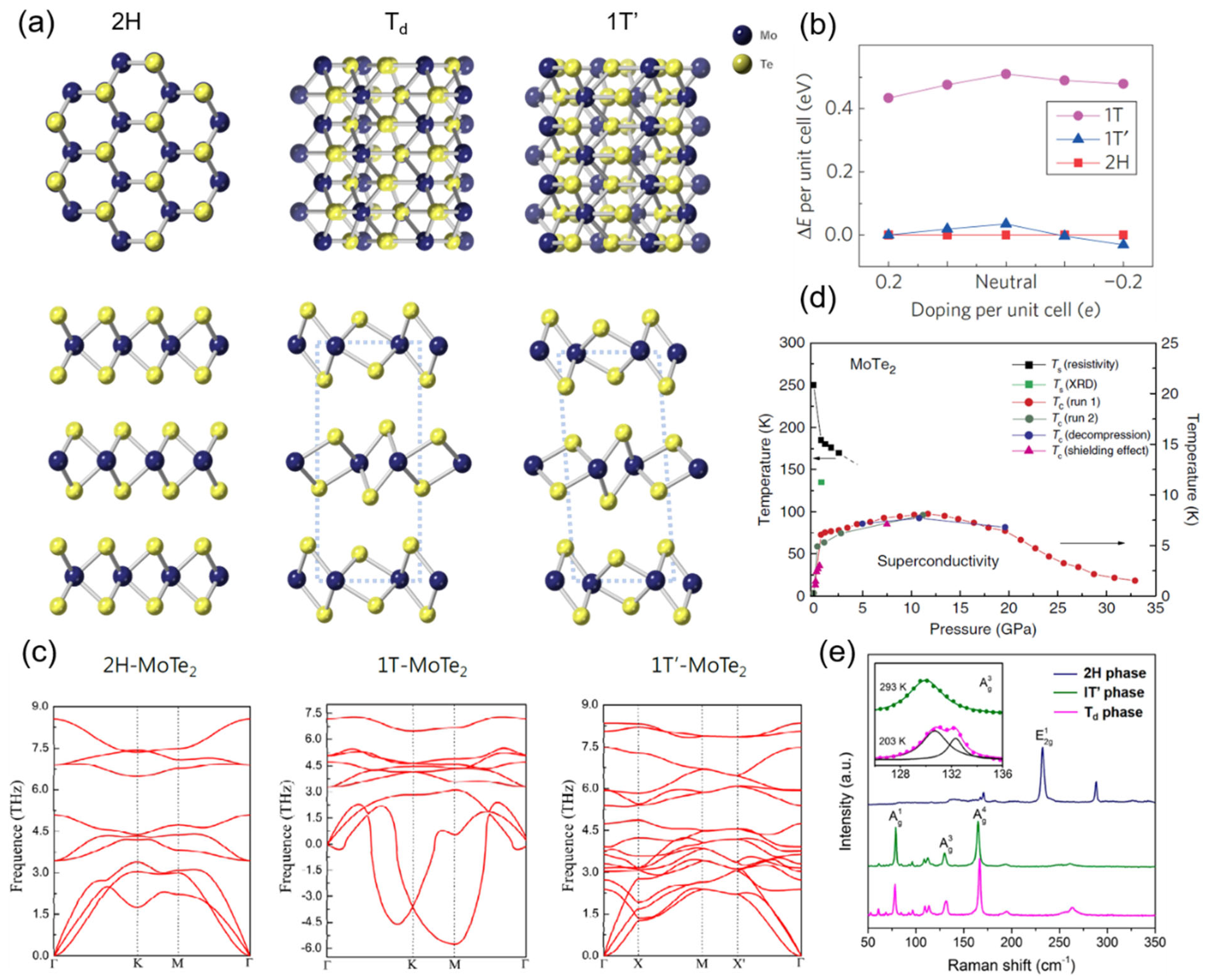
Figure 1. Structures and properties of different phases of MoTe2. (a) Atomic models of 2H-, Td-, and 1T′-MoTe2; (b) relative total energy per unit cell for 1T-, 1T′-, and 2H-MoTe2 with different electron doping levels (c) phonon dispersion curves of 2H-, 1T-, and 1T′-MoTe2, Reprinted with permission from [13] 2015 Springer Nature.; (d) electronic phase diagram of MoTe2 extracted from various measurements, Reprinted with permission from [17] 2016 Springer Nature; (e) Raman spectra of 2H-, 1T′-, and Td-MoTe2.
2. Phases and Properties of MoTe2
Near room temperature, MoTe2 exhibits three stable phases: 2H, 1T′, and Td phases. These phases have different lattice structures, band structures, and fingerprints in optical spectra.
2.1. 2H Phase
As shown in Figure 1a, 2H-MoTe2 (α-phase) exhibits a hexagonal structure, and it belongs to the space group P63/mmc with a honeycomb-like in-plane structure [18]. In addition, 2H-MoTe2 is an indirect bandgap semiconductor (bandgap 0.8 eV [19]) in bulk and few-layer states (Figure 1c). When thinned to a monolayer, however, it becomes a direct bandgap semiconductor (bandgap 1.1 eV [20]). Generally, 2H-MoTe2 is relatively stable in ambient conditions, but, due to the extremely small energy barrier with 1T′-MoTe2, it will convert into the 1T′ phase under excess Te deficiency or strain [21][22].
2.2. 1T′ Phase
Firstly, 1T′-MoTe2 (β-phase) has a monolithic structure, belonging to space group P21/m, with a distorted centered honeycomb in-plane structure and slightly inclined interplane structure (β angle = 93°55′) [18], as shown in Figure 1a. Compared to 2H-MoTe2, 1T′-MoTe2 is more vulnerable to oxidation [23]. In addition, 1T′-MoTe2 is generally acknowledged to be metallic, whether in the bulk or monolayer state. However, there are some reports designating few-layer 1T′-MoTe2 as a semiconductor. Keum et al. reported that few-layer 1T′-MoTe2 exhibited a bandgap opening up to 60 meV (Figure 1c) and proposed that it was induced by strong spin–orbit coupling (SOC) [13]. More recently, tri-layer 1T′-MoTe2 was reported to possess a narrow bandgap of 28 meV, but, in thicker MoTe2 samples (>4 nm), such bandgap opening was not observed [24]. On the contrary, it was also reported that tri-layer 1T′-MoTe2 remained free of a bandgap [25]. It is still under debate whether few-layer 1T′-MoTe2 has a bandgap.
In addition, 1T′-MoTe2 was reported to be a topological insulator as well as a room-temperature ferroelectric material. A weak antilocalization effect was observed in monolayer 1T′-MoTe2, indicating the presence of strong SOC, which is related to topological insulator materials [26]. Bulk 1T′-MoTe2 was predicted to be a Z4-nontrivial higher-order TI (HOTI) driven by double band inversion [27], which has not been experimentally confirmed yet. Recently, robust room-temperature out-of-plane ferroelectricity was observed in monolayer distorted 1T-MoTe2 [28], which has sparked the exploration of fundamental physics and promising applications at the monolayer limit.
2.3. Td Phase
Td-MoTe2 (γ-phase) has an orthogonal structure, belonging to space group Pmn21 [18]. Compared to the 1T′ phase, the Td phase displays a very similar but more regular structure (Figure 1a). From the cross-section direction, atoms in different layers of Td-MoTe2 are in good alignment with each other, whereas, in 1T′-MoTe2 atoms, layers slide a short distance and form a 0.94° tilt angle. Therefore, it is almost impossible to distinguish 1T′ from Td MoTe2 at the level of the monolayer.
When the temperature is increased above ~250 K, the Td phase is supposed to convert to the 1T′ phase [29]. In order to obtain stable Td-MoTe2 at room temperature, tungsten substitutional doping [30] and thinning the material to be below 10 nm [29][31] are effective strategies. Owing to its broken inversion symmetry, the Td phase possesses abundant physical properties, such as superconductivity and Type-II WSM.
Td-MoTe2 exhibits pressure- and thickness-dependent superconductivity. The transition temperature Tc of Td-MoTe2 increases with higher pressure and smaller thickness. The Tc of bulk Td-MoTe2 was reported to be 0.10 K (Figure 1d) [17]. Guguchia et al. observed the two-gap s-wave symmetry of the superconducting order parameter in Td-MoTe2, and suggested a higher possibility of a topologically non-trivial s+− state in Td-MoTe2 [32]. A fast-mode oscillation of the critical current Ic versus magnetic field B along the edge was observed in Td-MoTe2 by Wang et al., which was generated by fluxoid quantization and indicated the existence of a robust edge supercurrent [33]. As the breaking of the time-reversal symmetry or inversion symmetry is the prerequisite for WSM, Td-MoTe2 was predicted as a Type-II WSM due to its noncentrosymmetric lattice structure [34]. Kaminski et al. identified Fermi arcs, Weyl points, and novel surface states in bulk Td-MoTe2 with the angle-resolved photoemission spectroscopy (ARPES) technique, providing experimental evidence for Td-MoTe2 as a Type-II WSM [35]. Large magnetoresistance, a chiral-anomaly-related phenomenon, was reported in Td-MoTe2, further proving that Td-MoTe2 is a representative Type-II WSM [36][37].
3. Construction of 2D MoTe2 Hetero-Phase Homojunctions
3.1. Direct Synthesis
Chemical vapor deposition (CVD) is a universal and convenient method for the direct synthesis of 2D materials and heterojunctions, which is also viable in the case of MoTe2 hetero-phase homojunctions. The key to constructing 2D MoTe2 hetero-phase homojunctions is precise control of phases. The final phase of MoTe2 after growth is determined by several factors, which are growth temperature, growth atmosphere, and Te vacancy concentration.
It was reported that the most thermodynamically stable phase varied under different processing temperatures [38]. Thus, by controlling the growth temperature, a certain phase can be selectively obtained. Sung et al. reported that the 1T′-phase was the dominant product at a higher temperature (710 °C), and the 2H phase dominated at a lower temperature (670 °C) [12]. By sequential growth of 1T′ and 2H-MoTe2, they obtained isolated lateral 1T′-2H-MoTe2 homojunctions (Figure 2a). With increasing temperature, Yang et al. observed the phase evolution shown in Figure 2c: pure 1T′-phase→1T′- and 2H-phase→pure 2H-phase→2H- and 1T′-phase→pure 1T′-phase [39].
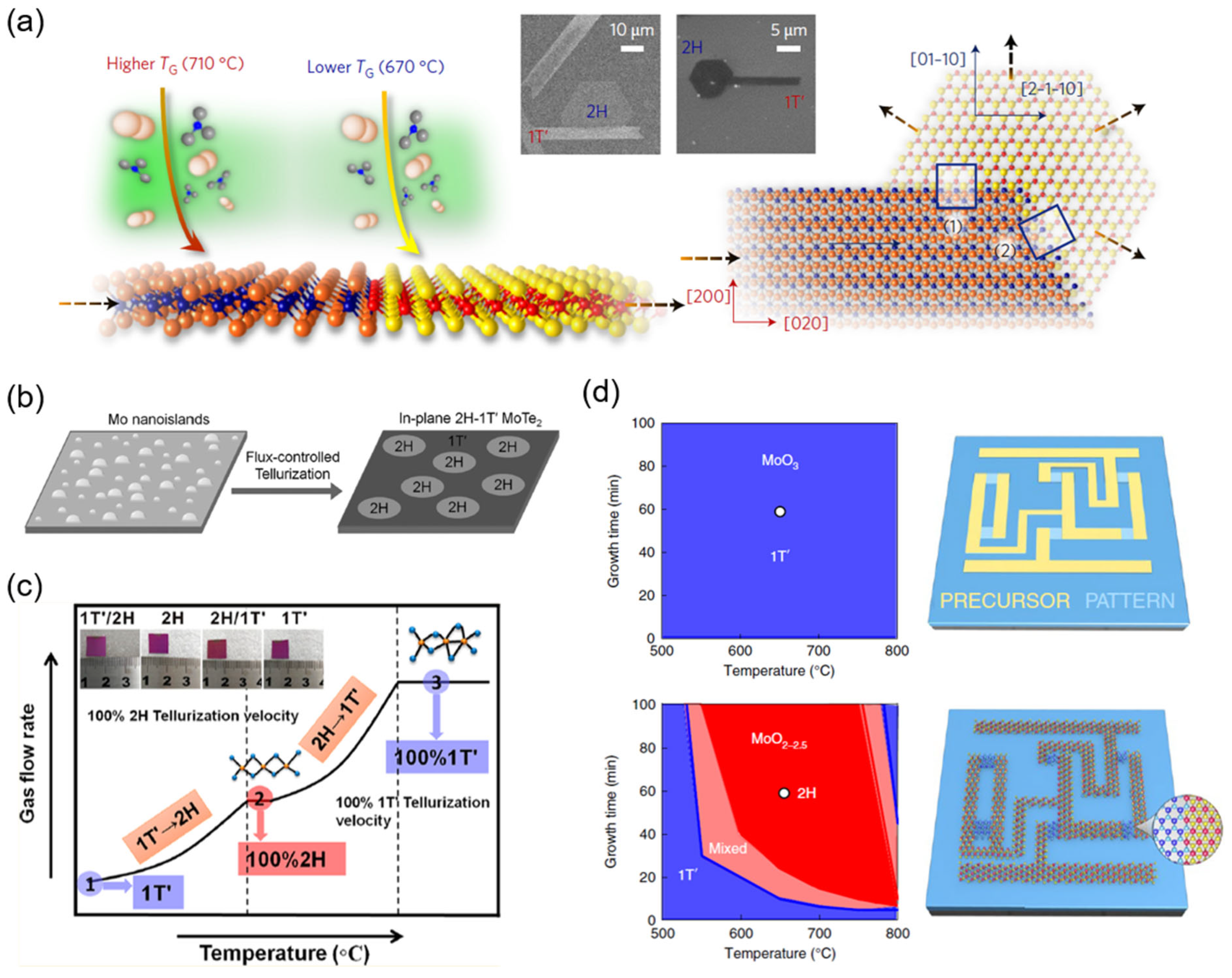
Figure 2. Direct synthesis of MoTe2 hetero-phase homojunctions. (a) Controlling growth temperature, Reprinted with permission from [12] 2017 Springer Nature; (b) flux-controlled tellurization Reprinted with permission from [38] 2017 John Wiley and Sons; (c) controlling growth temperature and gas flow rate Reprinted with permission from [39] 2017 American Chemical Society; (d) simultaneous tellurization of patterned precursors with different compositions.
3.2. Post-Processing
Besides direct synthesis, post-processing is also a very versatile strategy to realize 2D MoTe2 hetero-phase homojunctions. Owing to the small energy barrier between the 2H and 1T′ phases, external stimuli, such as a laser, electrostatic gating, mechanical deformations, chalcogen alloying, and lithium-ion (Li+) intercalation, can easily induce phase transition in MoTe2.
Laser treatment was reported to induce Te vacancies in MoTe2, which thereafter triggered the local phase transition from the 2H phase to 1T′ phase [40][41][42]. Cho et al. used laser-induced phase patterning to fabricate an ohmic 2H–1T′ hetero-phase homojunction that was stable up to 300 °C (Figure 3a) [40]. Not only an ohmic contact between phases but also a patterned phase transfer area could be achieved by this method. By carefully adjusting the laser power and irradiation time, the structural phases of MoTe2 could be gradually controlled [43].

Figure 3. Construction of MoTe2 hetero-phase homojunctions via post-processing. (a) Laser-induced phase patterning, Reprinted with permission from [40] 2015 The American Association for the Advancement of Science; (b) writing monolithic IC on 2H-MoTe2 with a scanning visible light probe, Reprinted with permission from [44] 2018 Springer Nature; (c) schematic diagram and (d) phase stabilities of monolayer MoTe2 under electrostatic gating at constant stress in a capacitor structure, Reprinted with permission from [45] 2016 Springer Nature; (e) phase evolution under tensile mechanical deformation, Reprinted with permission from [46] 2014 Springer Nature; (f) phase diagram of W alloyed MoTe2.
4. Applications of 2D MoTe2 Hetero-Phase Homojunctions
4.1. Electronic Devices
Transistors with ohmic contacts have always been in great demand in the semiconductor industry due to their high performance and low power consumption [47][48]. However, the external metal electrodes in transistors tend to induce not only high SBH, resulting from Fermi-level pinning, but also impurities and defects owing to the multi-step procedures of device fabrication, which leads to severe deterioration in device performance [49]. Two-dimensional MoTe2 hetero-phase homojunctions provide a solution to these problems. Owing to the small energy barrier between the metallic 1T′ phase and semiconducting 2H phase, the coexistence of the two phases is attainable in transistors as electrodes and channels, respectively. If covalently bonded and atomically coherent, the hetero-phase interface in MoTe2 is anticipated to possess an ultralow SBH [12], which incidentally avoids contamination introduced by external metal contacts and unnecessary film depositions. Thus, there are high hopes for 2D MoTe2 hetero-phase homojunctions in applications involving electronic devices.
4.2. Optoelectronic Devices
As is mentioned above, few-layer 2H-MoTe2 possesses an indirect bandgap of 0.8 eV, which is suitable for near-infrared (NIR) photodetection [50]. The photogating effect was considered to dominate the photocurrent generation in few-layer 2H-MoTe2-based photodetectors and the detailed mechanism was demonstrated as follows: after the generation of electron–hole pairs under irradiation, the charged trap states in the channel acted as a local floating gate and induced more electrons by trapping holes, leading to effective tuning of the channel conductance [51][52].
For MoTe2 hetero-phase homojunctions, photodetectors with both lateral and vertical structures were reported. Via a two-step patterned CVD growth and transfer method, Xu et al. fabricated a lateral 1T′–2H–1T′-MoTe2 hetero-phase FET array on a flexible polyimide substrate [53]. They measured the NIR photoresponsivity of the hetero-phase photodetector under different incident light powers and showed a high NIR photoresponsivity of ~1.02 A/W (Figure 4a–c). Lin et al. constructed a vertical 1T′–2H-MoTe2 hetero-phase photodetectors and compared the optical response properties to that without inserting 1T′-MoTe2 interlayer contact [54].
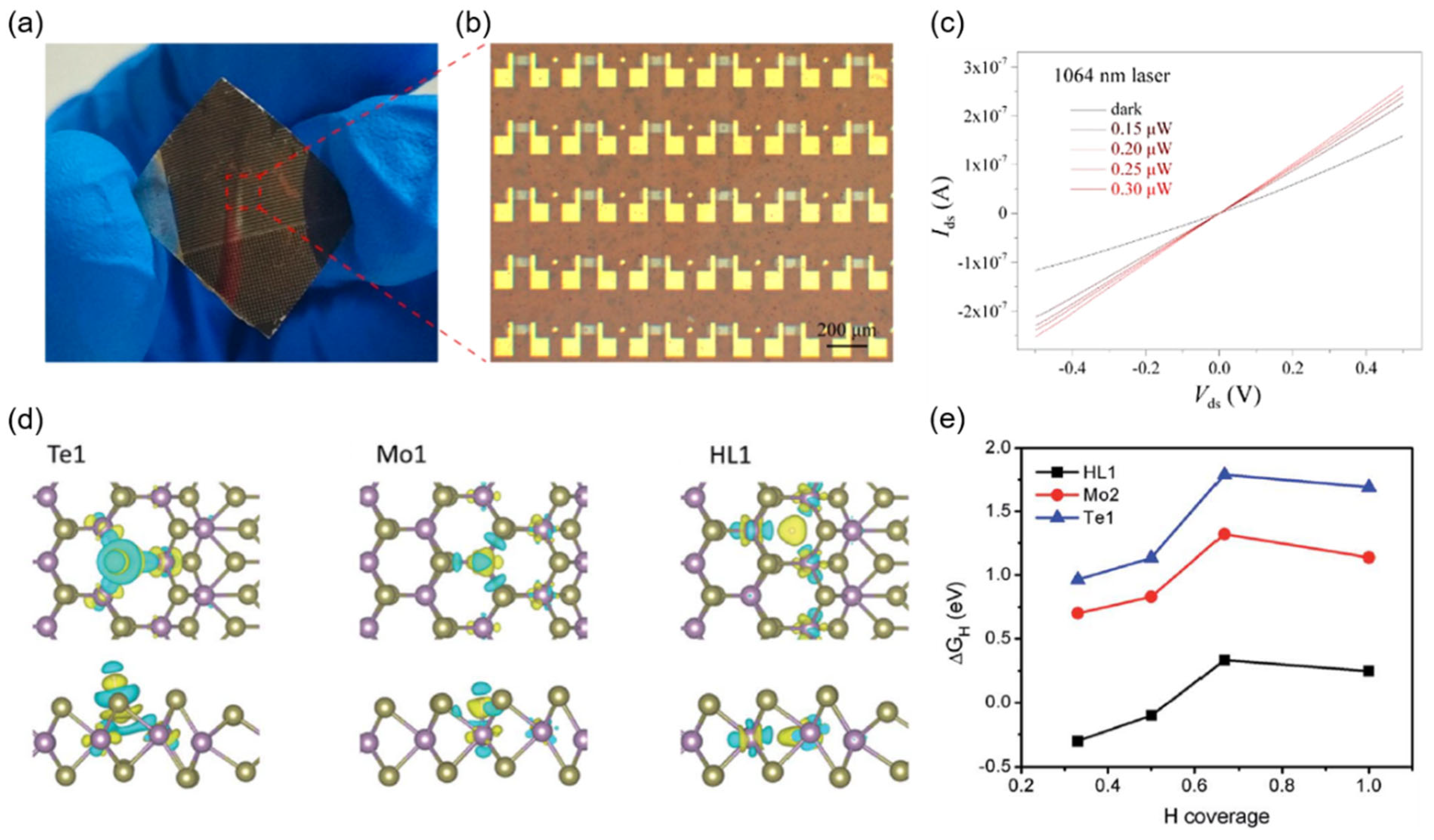
Figure 4. Applications of MoTe2 hetero-phase homojunctions in optoelectronic devices and electrocatalysis. (a) Macroscopic photograph, (b) magnified optical microscope image, and (c) I–V curves of hetero-phase MoTe2 photodetectors, Reprinted with permission from [53] 2019 American Chemical Society; (d) charge distribution contour plots of hydrogen adsorption sites at the MoTe2 phase boundary, Reprinted with permission from [55] 2013 Royal Society of Chemistry; (e) plot of Gibbs free energy versus hydrogen coverage for hydrogen adsorption sites.
4.3. Electrocatalysis Materials
Furthermore, 1T′-MoTe2 was reported to have significant potential in electrocatalysis. Resulting from the adsorption of H atoms onto Te sites on the surface, 1T′-MoTe2 exhibited a rapid and reversible activation process where the overpotential required to maintain a certain current density decreased significantly when held at cathodic bias [56].
Chen et al. illustrated that 2H–1T′ phase boundaries could effectively activate the basal plane of monolayer MoTe2 for enhanced hydrogen evolution reaction (HER) performance [55]. They investigated, by first-principles calculations, the structural and energetics stabilities of possible configurations of the 2H–1T′ phase boundary, including Te, Mo, and hollow sites, which were identified as possible catalytic centers for the HER at energetically stable phase boundaries (Figure 4d). In particular, the hollow sites newly induced by phase boundaries exhibited comparable Gibbs free energy to that of Pt near the thermoneutral value for H2 adsorption (Figure 4e), which was due to the unique electronic structures and local geometries of H2 adsorption at phase boundaries.
References
- Moore, G.E. Cramming more components onto integrated circuits, Reprinted from Electronics, volume 38, number 8, April 19, 1965, pp.114 ff. IEEE Solid-State Circuits Soc. Newsl. 2006, 11, 33–35.
- Packan, P.A. Pushing the Limits. Science 1999, 285, 2079–2081.
- Lundstrom, M. Applied physics. Moore’s law forever? Science 2003, 299, 210–211.
- Young, K.K. Short-channel effect in fully depleted SOI MOSFETs. IEEE Trans. Electron. Devices 1989, 36, 399–402.
- Bin, Y.; Wann, C.H.J.; Nowak, E.D.; Noda, K.; Chenming, H. Short-channel effect improved by lateral channel-engineering in deep-submicronmeter MOSFET′s. IEEE Trans. Electron. Devices 1997, 44, 627–634.
- Bar-Yam, Y.; Joannopoulos, J.D. Dangling bond in a-Si:H. Phys. Rev. Lett. 1986, 56, 2203–2206.
- Zhang, S.B.; Wei, S.H. Surface energy and the common dangling bond rule for semiconductors. Phys. Rev. Lett 2004, 92, 086102.
- Liu, Y.; Duan, X.; Shin, H.J.; Park, S.; Huang, Y.; Duan, X. Promises and prospects of two-dimensional transistors. Nature 2021, 591, 43–53.
- Tung, R.T. The physics and chemistry of the Schottky barrier height. Appl. Phys. Rev. 2014, 1, 011304.
- Manzeli, S.; Ovchinnikov, D.; Pasquier, D.; Yazyev, O.V.; Kis, A. 2D transition metal dichalcogenides. Nat. Rev. Mater. 2017, 2, 17033.
- Zhang, Q.; Wang, X.-F.; Shen, S.-H.; Lu, Q.; Liu, X.; Li, H.; Zheng, J.; Yu, C.-P.; Zhong, X.; Gu, L.; et al. Simultaneous synthesis and integration of two-dimensional electronic components. Nat. Electron. 2019, 2, 164–170.
- Sung, J.H.; Heo, H.; Si, S.; Kim, Y.H.; Noh, H.R.; Song, K.; Kim, J.; Lee, C.S.; Seo, S.Y.; Kim, D.H.; et al. Coplanar semiconductor-metal circuitry defined on few-layer MoTe2 via polymorphic heteroepitaxy. Nat. Nanotechnol. 2017, 12, 1064–1070.
- Keum, D.H.; Cho, S.; Kim, J.H.; Choe, D.-H.; Sung, H.-J.; Kan, M.; Kang, H.; Hwang, J.-Y.; Kim, S.W.; Yang, H.; et al. Bandgap opening in few-layered monoclinic MoTe2. Nat. Phys. 2015, 11, 482–486.
- Sun, Y.; Pan, J.; Zhang, Z.; Zhang, K.; Liang, J.; Wang, W.; Yuan, Z.; Hao, Y.; Wang, B.; Wang, J.; et al. Elastic Properties and Fracture Behaviors of Biaxially Deformed, Polymorphic MoTe2. Nano Lett. 2019, 19, 761–769.
- Mortazavi, B.; Berdiyorov, G.R.; Makaremi, M.; Rabczuk, T. Mechanical responses of two-dimensional MoTe2; pristine 2H, 1T and 1T′ and 1T′/2H heterostructure. Extreme Mech. Lett. 2018, 20, 65–72.
- Zhang, Y.-J.; Wang, R.-N.; Dong, G.-Y.; Wang, S.-F.; Fu, G.-S.; Wang, J.-L. Mechanical properties of 1T-, 1T′-, and 1H-MX2 monolayers and their 1H/1T′-MX2 (M = Mo, W and X = S, Se, Te) heterostructures. AIP Adv. 2019, 9, 125208.
- Qi, Y.; Naumov, P.G.; Ali, M.N.; Rajamathi, C.R.; Schnelle, W.; Barkalov, O.; Hanfland, M.; Wu, S.C.; Shekhar, C.; Sun, Y.; et al. Superconductivity in Weyl semimetal candidate MoTe2. Nat. Commun. 2016, 7, 11038.
- Dawson, W.G.; Bullett, D.W. Electronic structure and crystallography of MoTe2 and WTe2. J. Phys. C Solid State Phys. 1987, 20, 6159–6174.
- Zhang, F.; Zhang, H.; Krylyuk, S.; Milligan, C.A.; Zhu, Y.; Zemlyanov, D.Y.; Bendersky, L.A.; Burton, B.P.; Davydov, A.V.; Appenzeller, J. Electric-field induced structural transition in vertical MoTe2- and Mo1−xWxTe2-based resistive memories. Nat. Mater. 2019, 18, 55–61.
- Ruppert, C.; Aslan, O.B.; Heinz, T.F. Optical properties and band gap of single- and few-layer MoTe2 crystals. Nano Lett. 2014, 14, 6231–6236.
- Tang, Q. Tuning the phase stability of Mo-based TMD monolayers through coupled vacancy defects and lattice strain. J. Mater. Chem. C 2018, 6, 9561–9568.
- Zhu, H.; Wang, Q.; Cheng, L.; Addou, R.; Kim, J.; Kim, M.J.; Wallace, R.M. Defects and Surface Structural Stability of MoTe2 Under Vacuum Annealing. ACS Nano 2017, 11, 11005–11014.
- Yang, L.; Wu, H.; Zhang, W.; Chen, Z.; Li, J.; Lou, X.; Xie, Z.; Zhu, R.; Chang, H. Anomalous oxidation and its effect on electrical transport originating from surface chemical instability in large-area, few-layer 1T′-MoTe2 films. Nanoscale 2018, 10, 19906–19915.
- Park, J.C.; Jung, E.; Lee, S.; Hwang, J.; Lee, Y.H. Evidence of shallow band gap in ultrathin 1T′-MoTe2 via infrared spectroscopy. Phys. Rev. B 2020, 101, 235434.
- Song, P.; Hsu, C.; Zhao, M.; Zhao, X.; Chang, T.-R.; Teng, J.; Lin, H.; Loh, K.P. Few-layer 1T′ MoTe2 as gapless semimetal with thickness dependent carrier transport. 2D Mater. 2018, 5, 031010.
- Naylor, C.H.; Parkin, W.M.; Ping, J.; Gao, Z.; Zhou, Y.R.; Kim, Y.; Streller, F.; Carpick, R.W.; Rappe, A.M.; Drndic, M.; et al. Monolayer Single-Crystal 1T′-MoTe2 Grown by Chemical Vapor Deposition Exhibits Weak Antilocalization Effect. Nano Lett. 2016, 16, 4297–4304.
- Wang, Z.; Wieder, B.J.; Li, J.; Yan, B.; Bernevig, B.A. Higher-Order Topology, Monopole Nodal Lines, and the Origin of Large Fermi Arcs in Transition Metal Dichalcogenides XTe2 (X = Mo, W). Phys. Rev. Lett. 2019, 123, 186401.
- Yuan, S.; Luo, X.; Chan, H.L.; Xiao, C.; Dai, Y.; Xie, M.; Hao, J. Room-temperature ferroelectricity in MoTe2 down to the atomic monolayer limit. Nat. Commun. 2019, 10, 1775.
- Cui, J.; Li, P.; Zhou, J.; He, W.Y.; Huang, X.; Yi, J.; Fan, J.; Ji, Z.; Jing, X.; Qu, F.; et al. Transport evidence of asymmetric spin-orbit coupling in few-layer superconducting 1Td-MoTe2. Nat. Commun. 2019, 10, 2044.
- Rhodes, D.; Chenet, D.A.; Janicek, B.E.; Nyby, C.; Lin, Y.; Jin, W.; Edelberg, D.; Mannebach, E.; Finney, N.; Antony, A.; et al. Engineering the Structural and Electronic Phases of MoTe2 through W Substitution. Nano Lett. 2017, 17, 1616–1622.
- He, R.; Zhong, S.; Kim, H.H.; Ye, G.; Ye, Z.; Winford, L.; McHaffie, D.; Rilak, I.; Chen, F.; Luo, X.; et al. Dimensionality-driven orthorhombic MoTe2 at room temperature. Phys. Rev. B 2018, 97, 041410.
- Guguchia, Z.; von Rohr, F.; Shermadini, Z.; Lee, A.T.; Banerjee, S.; Wieteska, A.R.; Marianetti, C.A.; Frandsen, B.A.; Luetkens, H.; Gong, Z.; et al. Signatures of the topological s+- superconducting order parameter in the type-II Weyl semimetal Td-MoTe2. Nat. Commun. 2017, 8, 1082.
- Wang, W.; Kim, S.; Liu, M.; Cevallos, F.A.; Cava, R.J.; Ong, N.P. Evidence for an edge supercurrent in the Weyl superconductor MoTe2. Science 2020, 368, 534–537.
- Sun, Y.; Wu, S.-C.; Ali, M.N.; Felser, C.; Yan, B. Prediction of Weyl semimetal in orthorhombic MoTe2. Phys. Rev. B 2015, 92, 161107.
- Huang, L.; McCormick, T.M.; Ochi, M.; Zhao, Z.; Suzuki, M.T.; Arita, R.; Wu, Y.; Mou, D.; Cao, H.; Yan, J.; et al. Spectroscopic evidence for a type II Weyl semimetallic state in MoTe2. Nat. Mater. 2016, 15, 1155–1160.
- Chen, F.C.; Lv, H.Y.; Luo, X.; Lu, W.J.; Pei, Q.L.; Lin, G.T.; Han, Y.Y.; Zhu, X.B.; Song, W.H.; Sun, Y.P. Extremely large magnetoresistance in the type-II Weyl semimetal MoTe2. Phys. Rev. B 2016, 94, 235154.
- Lee, S.; Jang, J.; Kim, S.-I.; Jung, S.-G.; Kim, J.; Cho, S.; Kim, S.W.; Rhee, J.Y.; Park, K.-S.; Park, T. Origin of extremely large magnetoresistance in the candidate type-II Weyl semimetal MoTe2-x. Sci. Rep. 2018, 8, 13937.
- Empante, T.A.; Zhou, Y.; Klee, V.; Nguyen, A.E.; Lu, I.H.; Valentin, M.D.; Naghibi Alvillar, S.A.; Preciado, E.; Berges, A.J.; Merida, C.S.; et al. Chemical Vapor Deposition Growth of Few-Layer MoTe2 in the 2H, 1T′, and 1T Phases: Tunable Properties of MoTe2 Films. ACS Nano 2017, 11, 900–905.
- Yang, L.; Zhang, W.; Li, J.; Cheng, S.; Xie, Z.; Chang, H. Tellurization Velocity-Dependent Metallic-Semiconducting-Metallic Phase Evolution in Chemical Vapor Deposition Growth of Large-Area, Few-Layer MoTe2. ACS Nano 2017, 11, 1964–1972.
- Cho, S.; Kim, S.; Kim, J.H.; Zhao, J.; Seok, J.; Keum, D.H.; Baik, J.; Choe, D.-H.; Chang, K.J.; Suenaga, K.; et al. Phase patterning for ohmic homojunction contact in MoTe2. Science 2015, 349, 625–628.
- Peng, B.; Zhang, H.; Chen, W.; Hou, B.; Qiu, Z.-J.; Shao, H.; Zhu, H.; Monserrat, B.; Fu, D.; Weng, H.; et al. Sub-picosecond photo-induced displacive phase transition in two-dimensional MoTe2. Npj 2D Mater. Appl. 2020, 4, 14.
- Si, C.; Choe, D.; Xie, W.; Wang, H.; Sun, Z.; Bang, J.; Zhang, S. Photoinduced Vacancy Ordering and Phase Transition in MoTe2. Nano Lett. 2019, 19, 3612–3617.
- Tan, Y.; Luo, F.; Zhu, M.; Xu, X.; Ye, Y.; Li, B.; Wang, G.; Luo, W.; Zheng, X.; Wu, N.; et al. Controllable 2H-to-1T′ phase transition in few-layer MoTe2. Nanoscale 2018, 10, 19964–19971.
- Seo, S.-Y.; Park, J.; Park, J.; Song, K.; Cha, S.; Sim, S.; Choi, S.-Y.; Yeom, H.W.; Choi, H.; Jo, M.-H. Writing monolithic integrated circuits on a two-dimensional semiconductor with a scanning light probe. Nat. Electron. 2018, 1, 512–517.
- Li, Y.; Duerloo, K.-A.N.; Wauson, K.; Reed, E.J. Structural semiconductor-to-semimetal phase transition in two-dimensional materials induced by electrostatic gating. Nat. Commun. 2016, 7, 10671.
- Duerloo, K.A.; Li, Y.; Reed, E.J. Structural phase transitions in two-dimensional Mo- and W-dichalcogenide monolayers. Nat. Commun 2014, 5, 4214.
- Pelella, A.; Kharsah, O.; Grillo, A.; Urban, F.; Passacantando, M.; Giubileo, F.; Iemmo, L.; Sleziona, S.; Pollmann, E.; Madauss, L.; et al. Electron Irradiation of Metal Contacts in Monolayer MoS2 Field-Effect Transistors. ACS Appl. Mater. Interfaces 2020, 12, 40532–40540.
- Wang, B.; Luo, H.; Wang, X.; Wang, E.; Sun, Y.; Tsai, Y.-C.; Zhu, H.; Liu, P.; Jiang, K.; Liu, K. Bifunctional NbS2-Based Asymmetric Heterostructure for Lateral and Vertical Electronic Devices. ACS Nano 2020, 14, 175–184.
- Di Bartolomeo, A.; Grillo, A.; Urban, F.; Iemmo, L.; Giubileo, F.; Luongo, G.; Amato, G.; Croin, L.; Sun, L.; Liang, S.-J.; et al. Asymmetric Schottky Contacts in Bilayer MoS2 Field Effect Transistors. Adv. Funct. Mater. 2018, 28, 1800657.
- Luo, H.; Wang, B.; Wang, E.; Wang, X.; Sun, Y.; Liu, K. High-Responsivity Photovoltaic Photodetectors Based on MoTe2/MoSe2 van der Waals Heterojunctions. Crystals 2019, 9, 315.
- Huang, H.; Wang, J.; Hu, W.; Liao, L.; Wang, P.; Wang, X.; Gong, F.; Chen, Y.; Wu, G.; Luo, W.; et al. Highly sensitive visible to infrared MoTe2 photodetectors enhanced by the photogating effect. Nanotechnology 2016, 27, 445201.
- Luo, H.; Wang, B.; Wang, E.; Wang, X.; Sun, Y.; Li, Q.; Fan, S.; Cheng, C.; Liu, K. Phase-transition modulated, high-performance dual-mode photodetectors based on WSe2/VO2 heterojunctions. Appl. Phys. Rev. 2019, 6, 041407.
- Xu, X.; Liu, S.; Han, B.; Han, Y.; Yuan, K.; Xu, W.; Yao, X.; Li, P.; Yang, S.; Gong, W.; et al. Scaling-up Atomically Thin Coplanar Semiconductor-Metal Circuitry via Phase Engineered Chemical Assembly. Nano Lett. 2019, 19, 6845–6852.
- Lin, D.-Y.; Hsu, H.-P.; Liu, G.-H.; Dai, T.-Z.; Shih, Y.-T. Enhanced Photoresponsivity of 2H-MoTe2 by Inserting 1T-MoTe2 Interlayer Contact for Photodetector Applications. Crystals 2021, 11, 964.
- Chen, Y.; Ou, P.; Bie, X.; Song, J. Basal plane activation in monolayer MoTe2 for the hydrogen evolution reaction via phase boundaries. J. Mater. Chem. A 2020, 8, 19522–19532.
- McGlynn, J.C.; Dankwort, T.; Kienle, L.; Bandeira, N.A.G.; Fraser, J.P.; Gibson, E.K.; Cascallana-Matias, I.; Kamaras, K.; Symes, M.D.; Miras, H.N.; et al. The rapid electrochemical activation of MoTe2 for the hydrogen evolution reaction. Nat. Commun. 2019, 10, 4916.
More
Information
Subjects:
Nanoscience & Nanotechnology
Contributor
MDPI registered users' name will be linked to their SciProfiles pages. To register with us, please refer to https://encyclopedia.pub/register
:
View Times:
1.9K
Revisions:
2 times
(View History)
Update Date:
19 Jan 2022
Table of Contents


Notice
You are not a member of the advisory board for this topic. If you want to update advisory board member profile, please contact office@encyclopedia.pub.
OK
Confirm
Only members of the Encyclopedia advisory board for this topic are allowed to note entries. Would you like to become an advisory board member of the Encyclopedia?
Yes
No
${ textCharacter }/${ maxCharacter }
Submit
Cancel
Back
Comments
${ item }
|
${ item.createdUser.fullName }
${ item.createdAt }
${ item.vote }
${ item.reply }
Delete
${ reply.createdUser.fullName }
${ reply.createdAt }
${ reply.vote }
Delete
There is no reply to this comment~
${ item.replyTextCharacter }/${ item.replyMaxCharacter }
Submit
Cancel
More
No more~
There is no comment~
${ textCharacter }/${ maxCharacter }
Submit
Cancel
${ selectedItem.replyTextCharacter }/${ selectedItem.replyMaxCharacter }
Submit
Cancel
Confirm
Are you sure to Delete?
Yes
No