Submitted Successfully!
To reward your contribution, here is a gift for you: A free trial for our video production service.
Thank you for your contribution! You can also upload a video entry or images related to this topic.
Version Summary Created by Modification Content Size Created at Operation
1 + 2268 word(s) 2268 2021-12-22 04:37:16 |
2 format correction Meta information modification 2268 2022-01-08 08:04:24 | |
3 Remove from the EC "Structures for Engineering and Architecture" Meta information modification 2268 2022-03-28 08:11:57 |

Video Upload Options

Do you have a full video?

Confirm

Are you sure to Delete?
Cite
If you have any further questions, please contact Encyclopedia Editorial Office.
Myler, H. VLSI Structures for DNA Sequencing. Encyclopedia. Available online: https://encyclopedia.pub/entry/17831 (accessed on 29 March 2024).
Myler H. VLSI Structures for DNA Sequencing. Encyclopedia. Available at: https://encyclopedia.pub/entry/17831. Accessed March 29, 2024.
Myler, Harley. "VLSI Structures for DNA Sequencing" Encyclopedia, https://encyclopedia.pub/entry/17831 (accessed March 29, 2024).
Myler, H. (2022, January 06). VLSI Structures for DNA Sequencing. In Encyclopedia. https://encyclopedia.pub/entry/17831
Myler, Harley. "VLSI Structures for DNA Sequencing." Encyclopedia. Web. 06 January, 2022.
VLSI Structures for DNA Sequencing
Edit

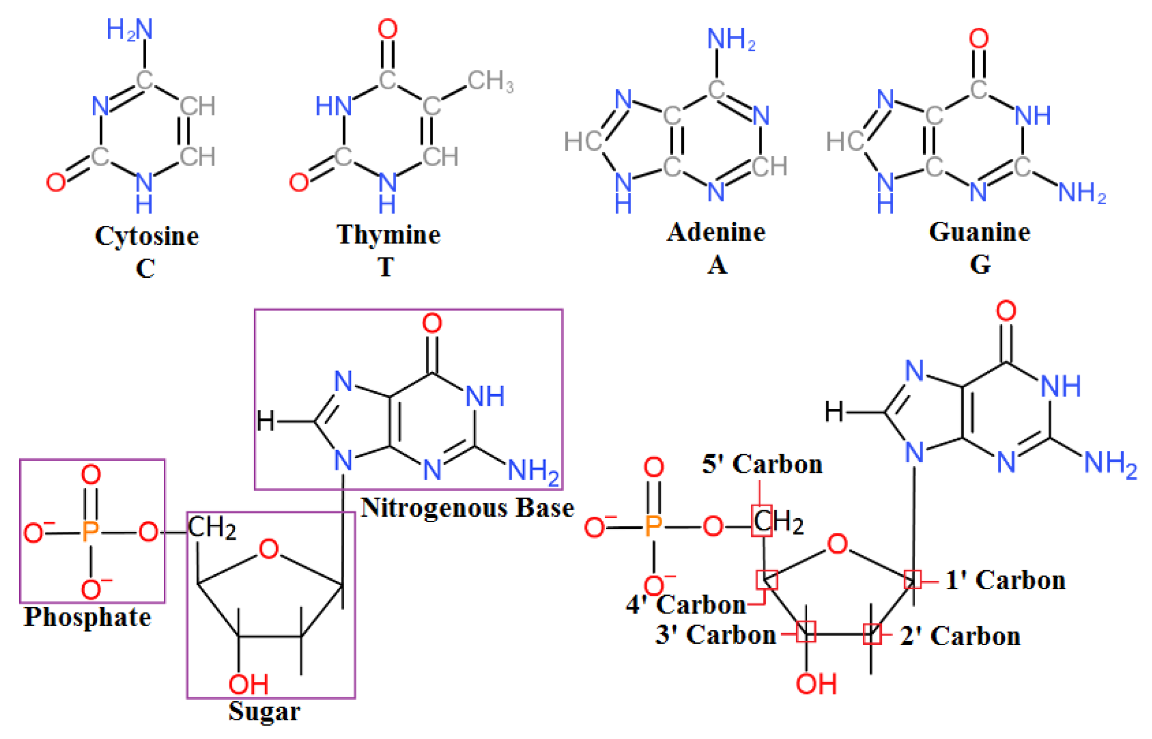
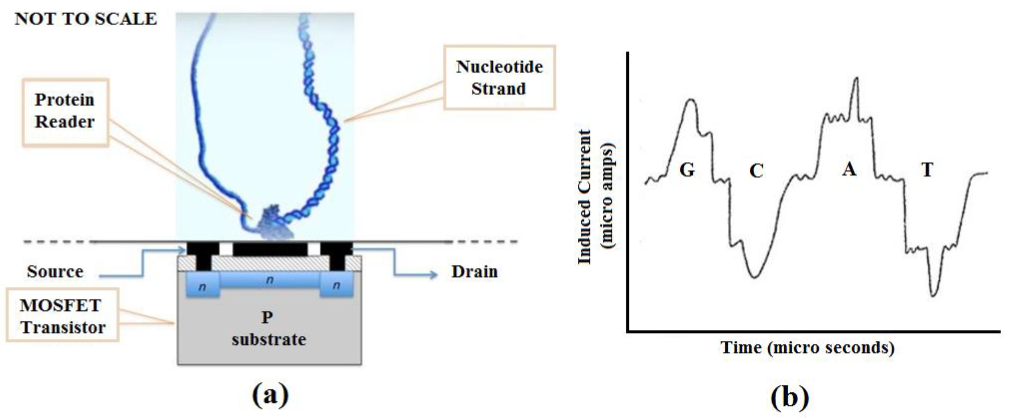
DNA sequencing is a critical functionality in biomedical research, and technical advances that improve it have important implications for human health. The overall structure of DNA is negatively charged and has a negative electrostatic potential due to a negatively charged phosphate backbone. Nucleotides are electroactive compounds that produce reduction and oxidation signals after hybridization. These high electrostatic potentials can be exploited with VLSI charge-sensitive electronic structures. The sequence of DNA is encoded within each nitrogenous base: adenine (A), guanine (G), cytosine (C), or thymine (T), and this 4-bit system allows for large amounts of information to be stored in a single DNA molecule, which may contain upward of 3 billion bases. 

DNA sequencing DNA hybridization DNA sensor GAA nanowire MOSFET

1. Introduction

Nucleic acids are the biomolecules that are essential for the continuity of all living organisms and store the hereditary information that passes from one generation to the next. This code for life is stored as deoxyribonucleic acid (DNA). DNA is composed of four basic nucleotides composed of a phosphate group, a sugar, and one of four different nitrogenous bases (Figure 1).
Figure 1. Four types of nitrogenous base and structure of a single nucleotide.
The overall structure of DNA is negatively charged and has a negative electrostatic potential due to a negatively charged phosphate backbone [1][2][3]. To know more about DNA’s structures and its molecular charge, readers are requested to consult [4][5][6]. Nucleotides are electroactive compounds that produce reduction and oxidation signals after hybridization [7]. These high electrostatic potentials can be exploited with VLSI charge-sensitive electronic structures. The sequence of DNA is encoded within each nitrogenous base: adenine (A), guanine (G), cytosine (C), or thymine (T), and this 4-bit system allows for large amounts of information to be stored in a single DNA molecule, which may contain upward of 3 billion bases. Reading this code from the DNA has provided and will continue to provide insights into genetic diseases, cancer, and the overall systems of the cell [8]. Therefore, DNA sequencing is a critical tool for biomedical research. Traditional DNA sequencing (Sanger sequencing) is performed by adding chain-terminating nucleotide analogs to a DNA synthesis reaction and then electrophoretically reading the mass or nucleotide added [9]. However, this sequencing is considered low-throughput and cannot access the large amount of information encoded in the human genome. Therefore, the development of more advanced techniques and sensors to detect and sequence DNA is necessary.
A biosensor is a device that can detect a biological substance or analyte by introducing it to a biological recognition element (receptor) and attaching the product to an appropriate transducer where the transducer converts the biological reaction into detectable or measurable signals; e.g., light, current, frequency, etc. There is significant interest in being able to detect and sequence DNA accurately, rapidly, and inexpensively for medical, forensic, and military purposes.

2. Limitations of Existing Technologies and Need for VLSI Biosensors for Sequencing

There are various high-throughput labeled and label-free DNA sequencing methods and technologies commercially available; some are for short-read sequencing and some are for long-read sequencing. Here, we list some of the limitations of the industry-leading high-throughput DNA sequencing technologies (Table 1 and Table 2). We will be covering some of the second-generation sequencing (SGS) or next-generation sequencing (NGS) methods, which are for short-read sequencing, and the third-generation sequencing for long-read sequencing.
Table 1. Limitations of short-read sequencing technologies.

Sequencing Method

Industry

Limitation

Ion semiconductor

Life Technologies

Homopolymer errors [10]

454 Pyrosequencing

ROCHE

Expensive and homopolymer errors [11]

Sequencing by synthesis (cyclic reversible termination)

Illumina, Qiagen

Expensive equipment [12]

Sequencing by ligation

Applied Biosystems (SOLiD)

Very slow, unable to read palindromic regions [13]

Table 2. Limitations of long-read sequencing technologies.

Sequencing Method

Industry

Limitation

Single-molecule real-time

Pacific Bioscience

Higher error rate, Low throughput, Expensive equipment [14]

Nanopore

ONT

Large error rate, Limitation on homopolymer sequencing [15]

Some limitations of short-read sequencing have overcome by third-generation sequencing approaches at the cost of high error rates. To learn more detail of the advantages and disadvantages of leading DNA sequencing technologies, readers are encouraged to consult [15].
The continuous optimization of CMOS for the purpose of improved computational and memory systems has enabled ultra-scaled devices. These nano-scaled devices also find use in the field of biosensing. There are a number of DNA hybridization detection/sensing techniques available in the literature; however, the use of Field Effect Transistors (FETs) is popular due to the great potential for miniaturization, fast responses, parallel sensing structures, and, most significantly, seamless integration with Complementary Metal Oxide Semiconductor (CMOS) processes. Using VLSI technologies such as CMOS processes, massively parallel integrated circuits can be created with high sensitivity that can be used for DNA sequencing detection. Additionally, a VLSI sensor can incorporate both the embedded analog and digital signal processing needed to increase performance and sensitivity and thus conserve power and reduce overall device size via System-On-Chip (SOC) technology. While DNA sequencing has been done by measuring the ion current through nanopores, incorporating CMOS technology to detect, amplify, and measure this current will improve the sequencing speed, size, and cost [16].

3. VLSI Architectures in DNA Detection

3.1. Electrolyte-Insulator Silicon (EIS) Capacitor

Fritz et al. developed a real-time and selective microfabricated FET sensor, which can detect the increase in the surface charge when the DNA hybridizes on the sensor surface. Their FET sensor is being developed using the Electrolyte-Insulator Silicon (EIS) capacitor structure using a silicon cantilever described in Cooper et al. [17]. Fritz and others chose to measure the capacitance as it requires only one electrical connection to the silicon. They immobilized the probe DNA on a poly-L-lysine (PLL) layer, which is positively charged and allows hybridization at low ionic strength. The reason is that at low ionic strength, this field-effect sensor is very sensitive [18]. The detection limit of their method is 2 nM, and it is mentioned that by using two similar sensors in parallel, it can detect a single base mismatch within a 12-mer oligonucleotide by differential detection techniques.

3.2. TFT (Thin Film Transistor)

Estrela et al. developed an Au/SiO2/Si MOS diode that is able to detect DNA hybridization by immobilizing the probe on the metal gate of the diode that is in contact with an electrolyte [19]. The immobilized DNA probe affects the interfacial dipole at the gate interface, which eventually influences the voltage drop across the electrochemical layer. This drop adjusts the voltage applied to the gate and changes the CV characteristics of the MOS diode. By observing the changes in C–V curve, it is possible to detect the DNA hybridization. Estrela and others also developed a Poly-Si TFT using the same principle that they used in the MOS diode, to detect DNA hybridization by observing changes in I–V characteristics of the fabricated device. They used a laser recrystallized film with an extended gate.

3.3. Different Types of FET’s

3.3.1. MOSFET (Metal Oxide Semiconductor FET)

Kim et al. fabricated a biosensor using 0.5 µm standard CMOS technology that can directly detect the intrinsic charge of the DNA. Using this FET-type DNA charge sensor, they were able to detect the immobilization and hybridization of the DNA probe by sensing the change in the drain current as the intrinsic charge of the immobilized DNA on the gate of the FET, which acts as the applied gate potential [20]. By considering the DNA charge as a Planer electrode charge, a relation between the gate voltage and the DNA charge is achieved).
where ρs = surface charge density (Cm−2); Ɛ0, Ɛ2, and Ɛ3 = dielectric constant (Fm−2) of vacuum, SiO2 and Si, respectively; and d2 and d3 = thickness (m) of SiO2 and Si respectively.

3.3.2. CMFET (Charge Modulated FET)

Barbaro and others [21] have proposed and simulated a Charge Modulated FET (CMFET) based on floating gate MOS transistors to detect the negatively charged oligonucleotides. The sensor has one control gate and one active area. The probes are immobilized on the surface of an active area surface, which provides the sensing charge. This surface charge will adjust the effective threshold voltage of the transistor predicted by [22]. The control gate is to nullify the unknown charge in the system. The effective threshold voltage can be measured by the drain current for a given control voltage or by measuring the control voltage for a constant drain current. During the hybridization, the charge amount on the sensor surface almost doubles as complementary strands attach to the probe and increase the effective threshold voltage. It is possible to raise the effective threshold voltage higher than the supply voltage by appropriately selecting the control gate voltage and other device parameters so that the device will not conduct. In such a manner, it is possible to detect the DNA hybridization by means of on/off signals of the CMFET.

3.3.3. ISFET (Ion Sensitive FET)

The Ion Sensitive FET (ISFET) was developed from MOSFET technology by removing the gate metal and submerging the silicon dioxide (SiO2) along with a reference electrode in an aqueous solution. See [23] for the working principle. In short, using an ISFET, the change in pH due to DNA hybridization can be detected because during the hybridization, hydrogen ions are being released, which reduces the pH of the reaction. An ISFET converts the chemical signals (H+) into electrical signals.

3.4. NWFET (Nanowire FET)

The fundamental principle of the semiconductor Nanowire (NW) FET (NWFET) sensor is explained in [24]. Among all the semiconductor NWs (Si, GaN, ZnO, SnO2, etc.), silicon NWs have distinct structural and chemical features such as diameters that are at the scale of proteins, their surface to volume ratio is high, and these features enable them to realize high performance FETs for sensitive biomolecular detection. Additionally, it is possible to control the electrical properties and sensitivity of the SiNWs by controlling the doping concentration and the diameter of the NWs [25].

3.5. Carbon Nanotube FET (CNTFET)

Single wall carbon nanotubes (SWNT) are made entirely of surface atoms, and the adsorption of molecules on SWNTs can significantly change the electrical properties of the SWNTs [26]. These changes are measured by observing the conductance or capacitance of the SWNTs, which are usually the gate materials of a FET sensor [27]. To integrate CNTs successfully into an electrical system, controlled deposition at a precise location and proper electrical contacts to metal leads are required. Readers are encouraged to review [28] to know more about the grafting of DNA onto SWCNTs and MWCNTs (Multi wall carbon nanotubes) and various characterization techniques adopted by various researchers, as well as [29] for the development of CNT-based FETs.

3.6. Graphene FET

Hwang et al. developed a fast, portable, and sensitive graphene FET sensor to detect SNPs. This graphene FET consists of two electrodes and a liquid gate chamber. Using this sensor, they were able to detect SNPs in large dsDNA, i.e., 47 nt [30]. They detected a single mismatch by strand displacement-induced resistance, i.e., current change and Dirac point shift in the graphene FET.

3.7. CMOS (Complementary Metal Oxide Semiconductor)

Lai et al. developed a sensor based on the method described in [21] for label-free DNA hybridization detection in a CMOS. They have used a layer of alumina as the passivation layer on top of the sensing/active area to ensure the reusability of the device. They were able to detect charges between 10−14 and 10−10 using their sensor, which includes the usual range of charges being generated during molecular and chemical reactions [31].

3.8. Nanopore FET

The combination of aa nanopore with a local FET to detect a single molecule that is translocating through the pore is very promising for DNA sequencing. Xie et al. developed a silicon nanowire FET, combining it with a solid-state nanopore to detect the change in electric potential due to the translocation of DNA molecules through the nanopore [32]. Bedell et al. proposed FET-based sensors for sequencing DNA and proteins that are embedded in a nanopore [33]. Their sensors can detect a change in drain current due to the passing of a DNA molecule through the nanopore. Moore et al. developed a nanopore FET in a CAD environment where a modeled nanopore and a gateless MOSFET were embedded in a cell membrane, accounting for the self-consistent Brownian dynamics and Drift-Diffusion techniques in a single simulation domain [34]. They were able to sense the movement of a single ion through the nanopore that can be used as a biosensor.

4. A Novel Method for DNA Sequencing

Due to the charged nature of the nucleotides, it is possible to detect a distinct charge signature for each individual base using a charge-sensitive device such as a MOSFET or other similar technology. Indeed, several groups have been able to detect DNA sequences using a pore on the gate of a MOSFET [35].
The researchers propose a nucleotide sequencing device that uses a MOSFET or similar electronic circuit technology to detect the charge signature of nucleotide bases as a target sequence is processed by a helicase, ribosome, or other polymerase motor protein. The color graphic inset figure (Figure 2a) illustrates the basic concept. A motor protein is affixed to a suitable substrate in contact with the gate region of a MOSFET or other charge-sensitive transistor. The motor protein is charged with the target nucleotide strand to be sequenced. The MOSFET is biased to reflect small charge variations as the nucleotide is processed by the protein motor, which acts as a driver to move the nucleotide data tape past the MOSFET gate serving as a read head. The signal produced by the MOSFET is then analyzed to elicit the GCAT sequence present in the nucleotide strand. Figure 2b, though not anticipatory, is from US 20130264204A9 [35] and shows how nucleotides develop unique signatures from induced current. Similar unique signatures will develop from charge variations that occur as the strand is passed across the charge-sensitive gate of the MOSFET.  A separate publication describing this technology in detail is in preparation.
Figure 2. (a) Proposed DNA sequencing device; (b) Charge representation of nucleotide bases [35].

References

  1. Rohs, R.; Jin, X.; West, S.; Joshi, R.; Honig, B.; Mann, R.S. Origins of specificity in protein-DNA recognition. Annu. Rev. Biochem. 2010, 79, 233–269.
  2. Lipfert, J.; Doniach, S.; Das, R.; Herschlag, D. Understanding nucleic acid-ion interactions. Annu. Rev. Biochem. 2014, 83, 813–841.
  3. Weiner, P.K.; Langridge, R.; Blaney, J.M.; Schaefer, R.; Kollman, P.A. Electrostatic potential molecular surfaces. Proc. Natl. Acad. Sci. USA 1982, 79, 3754–3758.
  4. Watson, J.D.; Crick, F.H.C. Reprint: Molecular structure of nucleic acids. Ann. Intern. Med. 2003, 138, 581.
  5. Frank-Kamenetskii, M.D.; Anshelevich, V.V.; Lukashin, A.V. Polyelectrolyte model of DNA. Uspekhi Fiz. Nauk 1987, 151, 595.
  6. Grosberg, A.Y.; Nguyen, T.T.; Shklovskii, B.I. Colloquium: The physics of charge inversion in chemical and biological systems. Rev. Mod. Phys. 2002, 74, 329–345.
  7. Paleček, E. Oscillographic polarography of highly polymerized Deoxyribonucleic acid. Nature 1960, 188, 656–657.
  8. Skogerboe, K.J. Molecular biology techniques. Anal. Chem. 1995, 67, 449–454.
  9. Men, A.E.; Wilson, P.; Siemering, K.; Forrest, S. Sanger DNA sequencing. In Next Generation Genome Sequencing: Towards Personalized Medicine; Wiley-VCH: Weinheim, Germany, 2008; ISBN 9783527320905.
  10. Feng, W.; Zhao, S.; Xue, D.; Song, F.; Li, Z.; Chen, D.; He, B.; Hao, Y.; Wang, Y.; Liu, Y. Improving alignment accuracy on homopolymer regions for semiconductor-based sequencing technologies. BMC Genom. 2016, 17, 521.
  11. Ronaghi, M. Pyrosequencing sheds light on DNA sequencing. Genome Res. 2001, 11, 3–11.
  12. Kircher, M.; Kelso, J. High-throughput DNA sequencing - Concepts and limitations. BioEssays 2010, 32, 524–536.
  13. Huang, Y.F.; Chen, S.C.; Chiang, Y.S.; Chen, T.H.; Chiu, K.P. Palindromic sequence impedes sequencing-by-ligation mechanism. BMC Syst. Biol. 2012, 6, S10.
  14. Rhoads, A.; Au, K.F. PacBio Sequencing and its applications. Genom. Proteom. Bioinforma 2015, 13, 278–289.
  15. Goodwin, S.; McPherson, J.D.; McCombie, W.R. Coming of age: Ten years of next-generation sequencing technologies. Nat. Rev. Genet. 2016, 17, 333–351.
  16. Magierowski, S.; Huang, Y.; Wang, C.; Ghafar-Zadeh, E. Nanopore-CMOS interfaces for DNA sequencing. Biosensors 2016, 6, 42.
  17. Cooper, E.B.; Fritz, J.; Wiegand, G.; Wagner, P.; Manalis, S.R. Robust microfabricated field-effect sensor for monitoring molecular adsorption in liquids. Appl. Phys. Lett. 2001, 79, 3875–3877.
  18. Fritz, J.; Cooper, E.B.; Gaudet, S.; Sorger, P.K.; Manalis, S.R. Electronic detection of DNA by its intrinsic molecular charge. Proc. Natl. Acad. Sci. USA 2002, 99, 14142–14146.
  19. Estrela, P.; Stewart, A.G.; Migliorato, P.; Maeda, H. Label-free detection of DNA hybridization with Au/SiO2/Si diodes and poly-Si TFTs. In Proceedings of the Technical Digest—International Electron Devices Meeting, San Francisco, CA, USA, 13–15 December 2004.
  20. Kim, D.S.; Jeong, Y.T.; Park, H.J.; Shin, J.K.; Choi, P.; Lee, J.H.; Lim, G. An FET-type charge sensor for highly sensitive detection of DNA sequence. Biosens. Bioelectron. 2004, 20, 69–74.
  21. Barbaro, M.; Bonfiglio, A.; Raffo, L. A charge-modulated FET for detection of biomolecular processes: Conception, modeling, and simulation. IEEE Trans. Electron Devices 2006, 53, 158–166.
  22. De Lumley-Woodyear, T.; Campbell, C.N.; Freeman, E.; Freeman, A.; Georgiou, G.; Heller, A. Rapid amperometric verification of PCR amplification of DNA. Anal. Chem. 1999, 71, 535–538.
  23. Bergveld, P. Short communications: development of an ion-sensitive solid-state device for neurophysiological measurements. IEEE Trans. Biomed. Eng. 1970, 70–71.
  24. Zhang, A.; Zheng, G.; Lieber, C. Nanowires : Building Blocks for Nanoscience and Nanotechnology; Springer International Publishing: Cham, Switzerland, 2016; ISBN 9783319419817.
  25. Cui, Y.; Duan, X.; Hu, J.; Lieber, C.M. Doping and electrical transport in silicon nanowires. J. Phys. Chem. B 2000, 104, 5213–5216.
  26. Snow, E.S.; Perkins, F.K.; Houser, E.J.; Badescu, S.C.; Reinecke, T.L. Chemical detection with a single-walled carbon nanotube capacitor. Science 2005, 307, 1942–1945.
  27. Mehrabani, S.; Maker, A.J.; Armani, A.M. Hybrid integrated label-free chemical and biological sensors. Sensors 2014, 14, 5890–5928.
  28. Daniel, S.; Rao, T.P.; Rao, K.S.; Rani, S.U.; Naidu, G.R.K.; Lee, H.Y.; Kawai, T. A review of DNA functionalized/grafted carbon nanotubes and their characterization. Sens. Actuators B Chem. 2007, 122, 672–682.
  29. Hu, P.A.; Zhang, J.; Li, L.; Wang, Z.; O’Neill, W.; Estrela, P. Carbon nanostructure-based field-effect transistors for label-free chemical/biological sensors. Sensors 2010, 10, 5133–5159.
  30. Michael, T.H.; Preston, B.L.; Joon, L.; Duyoung, C.; Alexander, H.M.; Gennadi, G.; Ratnesh, L. Highly specific SNP detection using 2D graphene electronics and DNA strand displacement. Proc. Natl. Acad. Sci. USA 2016, 13, 7088–7093.
  31. Lai, S.; Caboni, A.; Loi, D.; Barbaro, M. A CMOS biocompatible charge detector for biosensing applications. IEEE Trans. Electron Devices 2012, 59, 2512–2519.
  32. Xie, P.; Xiong, Q.; Fang, Y.; Qing, Q.; Lieber, C.M. Local electrical potential detection of DNA by nanowire-nanopore sensors. Nat. Nanotechnol. 2011, 7, 119–125.
  33. Bedell, S.; D’Emic, C.; Peng, H.; Zafar, S. FET Nanopore Sensor. U.S. Patent US8828138B2, 9 September 2014.
  34. Moore, I.; Millar, C.; Roy, S.; Asenov, A. FET based nano-pore sensing: A 3D simulation study. J. Comput. Electron. 2012, 11, 266–271.
  35. Sauer, J.; Zeghbroeck, J. Method and Apparatus for Detecting Nucleotides. U.S. Patent 20130264204A9, 10 October 2013.
More
Information
Contributor MDPI registered users' name will be linked to their SciProfiles pages. To register with us, please refer to https://encyclopedia.pub/register :
View Times: 520
Revisions: 3 times (View History)
Update Date: 28 Mar 2022
1000/1000