+1 credit
| Version | Summary | Created by | Modification | Content Size | Created at | Operation |
|---|---|---|---|---|---|---|
| 1 | Arijit Karmakar | + 4148 word(s) | 4148 | 2021-08-28 06:32:29 | | | |
| 2 | Conner Chen | Meta information modification | 4148 | 2021-09-23 02:51:09 | | |
Video Upload Options
Ionising radiation affects electronic circuits as well as living beings and has been a major concern for various critical applications such as healthcare, mining, avionics, nuclear, high-energy physics, and space applications. Radiation sensors are essential tools to estimate, measure and characterise radiation related information to assess the system performance and subsequently look for corrective measures.
1. Introduction
The radiation effects community, comprising physicists, medical researchers, nuclear reactors, and accelerator engineers, have long been working on analysing the effects of ionising radiation. Over the past few decades, several studies about the sources of radiation and the basic physics of radiation effects mechanisms [1][2] have facilitated the development of numerous radiation sensors. In the early 1960s and 1970s [3], the first set of basic radiation sensors were developed based on lead (plumbum) zirconium titanate ferroelectric materials [4], strain gauges [5], CaF2 thermal luminescent dosimeters [6], Si calorimeters [7], etc. These radiation sensors were mainly used for the measurement of absorbed dose and dose-rate related information. metal-oxide-semiconductor fieldeffect transistors (MOSFETs) devices were first identified to record the absorbed dose and applied as radiation sensors in the space environment in [8]. The phenomenon of single-event effects (SEEs), comprising the "funnelling" effect in silicon surface was discovered and experimentally illustrated in [9]. Following this, the quest for space explorations and satellite development put the focus on the implementation of another type of radiation sensor, namely the particle detector to identify the radiation induced faults in electronic systems. Over the course of time, the increased understanding of radiation interactions [10][11] and energy deposition processes have helped to extend the sensors with improved response coupled with new design techniques [12][13][14][15]. From the early 1980s, the theory of microdosimetry [16][17], particularly dealing with very low dose-level effects on microelectronics, was explored and studied with an emphasis on radiation oncology applications [18].
As silicon technology evolved, the downscaling of modern complementary metal-oxide-semiconductor (CMOS) technologies has made MOSFET devices less sensitive to cumulative radiation dose effects [19]. As the thickness of the gate-oxide has reduced, the rate of radiation induced hole trapping has gone down. Additionally, the generation of interface trap charges has decreased particularly due to electron tunnelling [20] and successive neutralisation of holes [21]. Eventually, the implementation of integrated radiation dosimeters in small feature sizes suffers extensively from reduced sensitivity. On the other hand, for scaled down CMOS technologies, the critical charge requirement to cause a single-event upset has reduced significantly [22][23]. As a result, the probability of the occurrence of SEEs in devices with lower feature sizes has increased [19]. This has favoured the development of integrated particle detectors with increased sensitivity.
2. Radiation Measurement Techniques
2.1. Silicon Diode Based Radiation Sensors
In this method, the reverse biased p-n junction of a diode is used for dosimetry measurement. The excess charges (minority carriers), which are created due to the interaction with ionising radiation near the depleted region, are swept away through drift in the presence of the electric field over the junction. As illustrated in Figure 1, the excess charges are collected with an external electric field and amplified using a charge-sensitive pre-amplifier. The resulting current or voltage transient from the amplified charge is compared with a threshold and shaped into a pulse to cause a trigger to the digital counter. Thus, while operating in pulse counting mode, the Si-diode based radiation sensors are used as particle detectors. Alternatively, in integral mode of operation a readout circuit measures the transient of voltage or current. The time-integral of the measured quantity provides an estimate of the energy deposited during radiation strike. Thereby, in dosimetry application this energy information provides an indirect measurement of the total accumulated dose on the sensing devices.
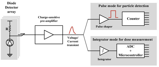
Figure 1. Illustrations of different methods (pulse mode and integral mode) of radiation detection of the Si-diode based radiation sensors.
Here, the diodes are configured in reverse bias mode of operation which in turn results in a wide depletion layer with reduced leakage current and thus permits higher efficiency in radiation sensing with a linear relationship between the deposited charge and the integrated dose. Si-diode based dosimeters such as single-sided silicon strip detectors [24] and active pixel detectors [25][26] are moderately sensitive and suitable for high-dose radiation measurement as in pulsed radiation fields (X-rays, electron linear accelerators) [27].
Over time, the sensitivity of the diodes reduces due to the damage caused by radiation and need to be re-calibrated to perform effective reliable measurements. During counting of radiation strikes, the readout time needs to be adjusted so that it is able to distinguish between concurrent events. In addition to particle detection and dose measurement, the intensity of the current transient provides an estimate about the energy spectra and linear energy transfer (LET) of the striking high energy particle. More often, an array of detectors is used, which is beneficial in terms of accuracy and to characterise the radiation beam.
2.2. Silicon Photodiodes Based Radiation Sensors
This type of radiation sensor uses Si-photodiodes as the sensing elements. Four types of photodiodes can be used for radiation measurement [28]: the p-n junction photodiode [29], the PIN (p-type, intrinsic, n-type) photodiode [30], the avalanche photodiode [31] and the Schottky photodiode [32]. Compared to standard p-n junction photodiodes, PIN photodiodes provide better sensitivity as the wide intrinsic region helps in achieving high charge generation per radiation strike. The highest sensitivity to radiation among photodiodes is usually obtained in Avalanche photodiodes due to the Avalanche breakdown action. However, the Avalanche photodiode based detectors need larger bias voltage and produce higher levels of noise. Schottky photodiode based radiation detectors are based on compound semiconductor structures (SiC) and provide a fast response time due to low operational capacitance.
The photodiodes can be integrated with SSPMs and are used as an alternate choice for vacuum-based photomultiplier tubes (PMTs) for space, nuclear energy plant and high-energy physics applications [33]. SSPMs are fabricated using an array of Geiger-mode photodiodes on custom CMOS technology. A radiation sensitive scintillator material is coupled to the fabricated SSPM device. An illustration of the CMOS SSPM chip coupled with scintillation material is provided in Figure 2. When an energised radiation particle impinges on the dosimeter surface, the scintillator absorbs the energy and re-emits it in the form of light. The generated photons hit the pixels in the SSPM matrix. A low LET ionising radiation strike activates a few pixels in the matrix, while in the case of a high LET radiation strike a large number of pixels are activated. In response to these, the scintillator coupled SSPM device produces an equivalent amount of current transient which is detected by the readout interface. Thereafter, the transients are recorded to count the radiation events. Similar to Si-diode based radiation sensors, the time integral of the current could also be digitised using an analogue-to-digital converter (ADC) to perform an indirect estimation of accumulated dose.
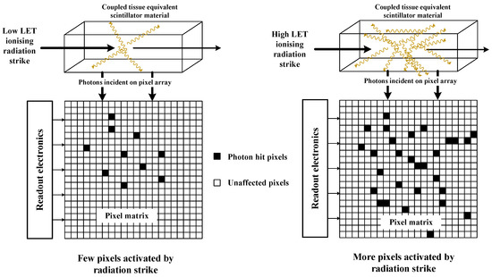
Figure 2. Illustration of working principle of scintillator coupled solid-state photomultiplier (SSPM) based dosimeter.
The number of photodiodes activated is proportional to the energy deposited due to the strike of high-energy radiation. Compared to PMTs, the SSPM based dosimeters are compact, lightweight and can be integrated with on-chip CMOS readout circuits [33][34]. The digitised output provides an estimation of the absorbed dose and deposited energy spectra and LET of the radiation particle.
2.3. Radiation Sensitive MOSFET Devices
The electrical characteristics of the MOSFET devices, particularly the mobility and the threshold voltage (VTH), experience changes due to the radiation strike from high-energy particles. The radiation induced field-oxide trapped charges produce a negative change in VTH for both pMOS and nMOS, whereas, in case of interface trap charges, pMOS see a negative change but nMOS sees a positive change in VTH [35]. Initially, the MOSFET based dosimeters were used in space [8] where the pMOS transistors were used in diode configuration to track and measure radiation dose by means of observing the VTH shift. A readout circuit was provided to track the voltage difference between the gate and source terminal (VGS) of the diode-mode pMOS transistors and to measure the change in threshold voltage. As predicted in [36], the absolute value of the threshold voltage shift is proportional to the gate-oxide thickness squared (t2OX). In order to increase the radiation sensitivity and ensure a better response, the RADFETs were provided with very thick gate oxide, which were used in nuclear facilities [37][38]. The devices were also used for radiation dosimetry in medical diagnosis and radiotherapy treatments [39][40]. The fabrication of RADFET devices require an ad hoc process, which makes it difficult to implement them with commercial CMOS technologies evolving to thinner oxides. The radiation sensitivity is also limited by the packaging materials. Additionally, the changing temperature effects of the MOSFET parameters (carrier mobility, VTH, etc.) make it difficult to isolate and identify radiation induced variations which in turn affects the accuracy of the dosimeter readings [41].
To overcome the lower sensitivity of the RADFET devices, FOXFETs are developed where the field oxide (used as the passivation layer to isolate CMOS circuits) is utilised instead of the gate oxides [42]. The thickness of the field oxide is usually in the range of 400–600 nm [42], and therefore it facilitates an increased amount of trapped charge generation when exposed to radiation. A view of the cross-section of the FOXFET device is provided in Figure 3a. Compared to RADFET devices, the higher number of trapped charges in FOXFET gate-oxide cause a much larger change in VTH. As shown in Figure 3b, the VTH of the FOXFET device is measured by forcing a constant current through the device and the VTH shift gives an estimate of the accumulated dose. The use of field oxide also made it easy to implement the device in any CMOS technology and integrate them together with the readout circuits. However, similar to RADFETs [43], the temperature dependency of the electrical parameters is still problematic with FOXFETs leading to erroneous dose readings. To mitigate the issues related to temperature variations, differential architectures are used where bias currents were designed with reduced temperature coefficients [44][45]. RADFET and FOXFET devices require very thick gate-oxide as well as large area to increase radiation sensitivity. These are therefore used as discrete devices or needed to be implemented in custom CMOS process.
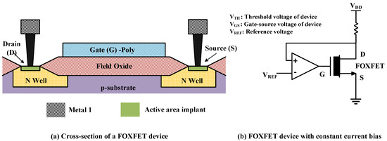
Figure 3. (a) Cross-section of a field-oxide field-effect transistor (FOXFET) device used in dosimeter and (b) readout circuit for threshold voltage measurement of a FOXFET based dosimeter.
Alternatively, FGMOS devices have also been explored for various dosimetry applications [15][46][47][48]. The floating gate (FG) structures can be implemented by connecting the poly-silicon gate of a MOS-capacitor to the gate of sensing MOSFET device in standard CMOS technology [49] as shown in in Figure 4a. Otherwise, it can also be implemented by using an additional insulated poly-silicon gate in a custom two poly CMOS process [50] as shown in Figure 4b. Thereby, in this process a capacitance is also formed alongside the gate of the FGMOS device. The capacitance is used to pre-charge the FG prior to irradiation by injection of carriers by avalanche process or by tunneling through the gate-oxide [47]. When exposed to ionising radiation, charges are generated which accumulate in the oxide region and neutralise the initial charge on the FG. This results in a change in VTH [46] and the readout circuit integrated on-chip with the sensing devices measures the VTH shift and provides a proportional voltage [48][51] or current output [52]. In order to compensate for temperature dependence of the VTH shift, a typical MOSFET with similar dimensions is used as a reference to monitor the temperature induced parameter variation. The sensing FGMOS and the typical MOSFET are used in a differential configuration and therefore it cancels out temperature induced changes happening in both devices as reported in [15][48]. Alternatively, the FGMOS devices are used to implement current starved inverters and provide a frequency output, the change of which is proportional to the total accumulated dose [49][50]. FGMOS based dosimeters are typically very sensitive to radiation dose and therefore the sensor responses are saturated and suffer from non-linearity for dose levels more than 100 Gy. These provide high resolution ( 500 mrad [50]), but the application of these sensors is only limited to low dose level (10–100 Gy) measurement. Compared to RADFET and FOXFET devices, FGMOS based radiation sensors are preferred in recent times considering the ease of on-chip integration with the peripheral circuits. FGMOS dosimeters are also being investigated for high-dose level monitoring in accelerator environments using the repeated measurement technique as reported in [53][54].
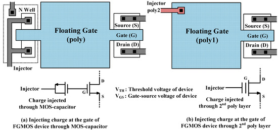
Figure 4. (a) Top view of the floating-gate MOSFET (FGMOS) device integrated with MOS-capacitor for charge injection into gate-oxide and (b) top view of the FGMOS device with an additional poly layer used for charge injection.
2.4. SRAM Based Radiation Monitor
In the presence of radiation hazards, SEUs can easily affect the circuits that store data, for example, flip-flop, RAM, and storage circuits. Among these, SRAM (Static Random-Access Memory) is the most typical circuit to monitor SEUs in electronic systems. It is composed of two cross-coupled inverters which create a stable bi-states structure, as shown in Figure 5. If one side of the circuit is hit by a particle, the collected charge from the particle will trigger the positive feedback of the inverters and lead to a bit flip (i.e., upset).
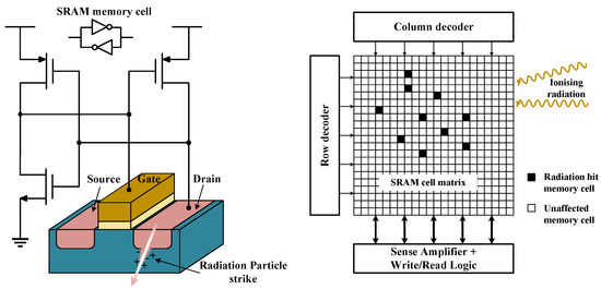
Figure 5. Mechanism of radiation strike and memory bit-flips on static random access memory (SRAM) nodes.
Moreover, SRAM is the most common device for SEU fault monitoring in processing systems. It has unique advantages such as a simple and controllable interface, low cost, high density (cells per unit area), low power consumption, and can be embedded on the same technology or chip as the device being monitored, like a microprocessor. The principle of SRAM based particle detectors is simply searching the memory for bit flips. These can be single-cell upsets (SCUs) or multi-cell upsets (MCUs). As technologies have scaled-down, single-particle strikes can upset multiple cells simultaneously, depending on the particle energy. As indicated in [55], the ratio of MCU and SCU can be used to estimate the particle energy.
The radiation detectors used in ESA [56], CERN [57], and satellite missions [58] have embedded multiple commercial off-the-shelf (COTS) SRAMs for SEU monitoring. The first purpose of these circuits is to monitor the radiation environment in space and ground facilities to guarantee that the environment radiation intensity is in line with the design specification of the system and the data are reliable. The second purpose is to monitor the flux, beam profile and beam homogeneity at particle accelerator facilities such as RADEF and CHARM [56]. Thirdly, for cross facility SEE testing, adding an SRAM to the system enables the cross-calibration of the variation at different facilities, which increases the data fidelity [59]. Fourthly, applying radiation-hardened devices improves the robustness to SEE. However, complex systems still inevitably contain COTS components to balance cost and performance. Therefore, an SEU monitor is needed for the system to guarantee the error rate of the system stays below the manageable limit.
To achieve a higher SEU sensitivity and resolution, SRAMs fabricated in smaller technology nodes (65 nm and less) can be used. In recent work [60][61], a broad variety of COTS SRAM chips and FPGAs were tested. The results showed that 16 to 65 nm SRAM have high SEU cross-sections. Alternatively, decreasing the supply voltage can increase the SEU sensitivity [62], and every type of particle shows a different sensitive range when varying the voltage supply [63]. This enables sufficient calibration for the radiation monitor to analyse the intensity and type of radiation source by sweeping the supply voltage [62][63]. However, commercial chips have an embedded voltage regulator between the voltage supply and the core circuit. This regulator can handle a certain range of input voltages to a constant level. It becomes nonlinear and unpredictable outside of its voltage range, especially for more advanced technologies. Henceforth, this approach is less feasible with commercial memories and calls for custom-designed SRAM sensors.
Finally, most COTS SRAMs have an embedded error-correcting code feature, which can correct some SEUs complicating or obstructing its use as a radiation monitor [64]. Additionally, when testing for MCUs, one needs to be aware that the physical order of the cell array may differ from the logical (address) order through scrambling. The susceptibility of COTS SRAM circuits to SEL-induced failures are more in comparison to custom-designed SRAM sensors. The COTS SRAM circuits are typically aimed to achieve a high density. Therefore, the wells and doping areas are closer than normal chips, making them more prone to latchup induced circuit failures.
2.5. Built-In Current Sensor Based Radiation Detectors
In this method, the radiation-induced transient current pulses are detected by means of monitoring the supply voltage [65][66][67] or measuring the supply current externally using current monitors [68][69]. The methods are not reliable and effective to identify the location of the transient induced logic state errors in an array of memory cells. The issue has been resolved by introducing built-in current sensor (BICS) circuits [70][71] adjacent to each row and column of the memory cell array to locate the transient induced faults. However, the proposed techniques involved distributed synchronous BICS circuits and subsequently failed to detect short and intermittent current transients in the supply. This method, as illustrated in Figure 6a, uses high-speed asynchronous BICS circuits which are placed in line with the power supply of the devices, and therefore it affects the system's performance by injecting noise and disturbances into the power supply.
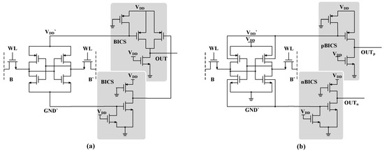
Figure 6. Built in current sensors connected to (a) power supply and (b) bulk of the devices.
As a remedy, a bulk connected BICS as shown in Figure 6b, is proposed in [72] with an increased sensitivity towards particle strike, but reduced interference with the system’s performance. The bulk connected BICS circuits consist of a pMOS activated BICS (pBICS) and an nMOS activated BICS (nBICS). At the onset of a radiation strike, the excess charges travel through the reversed biased bulk junction and activate the respective current sensors. Recently, similar approaches have been explored in [73][74][75][76][77][78] and a further improvement has been proposed in [79] by using triple-well CMOS technologies.
The primary advantage of utilising bulk connected BICS circuits is that they are able to locate transient induced faults and thus can effectively activate the mitigation mechanisms in the respective memory cells. However, it is ineffective in characterising the particle flux and suffers from the inability of directly providing any information about the deposited energy. Moreover, the current sensors are susceptible to substrate noise and subsequently may induce erroneous results.
2.6. 3-D NAND Flash Based Radiation Monitors
FGMOS devices have been exploited to realise various non-volatile memory architectures [80][81] and have been successfully explored for data storage applications in space [82][83][84]. In addition, the FG based devices are very effective in dosimetry applications to measure the amount of TID in a radiation environment [14][53][85]. Recently, the FG based flash memories appeared as a viable alternative [86][87][88] to be utilised as particle detectors.
As the ionising particle impinges on the devices in flash memories, the excess charge impacts the FG based storage element and subsequently cause threshold voltage shift in the FGMOS devices inside the memory cell. Nowadays, the readout circuits provided inside the flash memory cells can identify the radiation event from the change in threshold voltage and collectively measures the number of upsets similar to SRAM based radiation monitors. In the case of flash memory based architectures, each memory unit is configured with multi-bit (4-bit or 8-bit binary code) storage cells which are capable of measurement based characterisation of multi-level threshold voltage distributions. As a result, these types of particle detectors provide an estimate of charge deposited due to the interaction with radiation by accurately measuring the threshold voltage shifts [89]. Unlike the SRAM based solutions, it is feasible to characterise the LET of the striking particle in flash memories and extract information about the nature of radiation (heavy ion, proton [90], neutron [91]).
Due to the non-volatile nature of memory cells, the NAND flash-based particle detectors facilitate low power dissipation and offline passive mode of operation. Compared to 2-D structures, dense 3-D integration of flash memory cells is beneficial ensuring higher detection efficiency [92]. As illustrated in Figure 7, the affected memory elements provide the information about the angle of incidence and the track of radiation strike as well [93]. The further study of the pattern of the threshold voltage shifts of the devices arranged in a 3-D volume along the track of radiation strike provides more details about the uniformity of the ionising radiation beam [92][93].
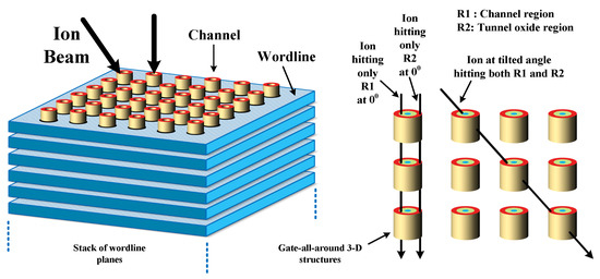
Figure 7. Mechanism of radiation strike on sensitive nodes of 3-D NAND flash.
Although the 3-D NAND flash-based particle detectors are beneficial in terms of efficiency and added features, the complexity of integration with planar CMOS technologies presents a difficulty in implementation. In addition, the device noise affects the accuracy of estimation of energy absorbed in radiation requiring complex readout schemes targeting low noise mixed-signal readout implementations [94]. Another notable drawback is the long readout time needed to process a very large number of memory cells which also leads to an increased expenditure of power.
2.7. Memristor Based Radiation Sensor
Memristor based resistive random-access-memory (ReRAM) technology has been brought into focus during the last decade [95][96] considering its non-volatile property and ability to perform in-memory computing both in digital and analog domain operations. Typically, a ReRAM cell consists of a memristor element, a two terminal non-linear resistive device prepared by sandwiching a resistive material (TiO2, ZrO2, NiO, etc.) between two metal electrodes. The value of its resistance (known as memresistance) is not constant and changes depending on the magnitude, polarity and duration time of the applied voltage across its terminals, or the current passed through it. It shows a hysteretic behaviour in its voltage-current characteristics and the memresistance value of the devices are non-volatile in nature.
Under ionising radiation, the electrical properties of the elements are subjected to change due to the processes through ionic and molecular dissociations and defect formations, unlike charge formation that happens in CMOS devices. The initial investigations [97][98][99] have showed very little dependence of memristor devices on radiation effects due to its ultra-thin film structures. However, “μm-thick” TiO2 based elements showcased increased radiation detection ability [100].
As illustrated in [100], each memristor is connected to a switched capacitor element to charge the capacitors. As shown in Figure 8, each memristor is switched on in monitoring mode using the voltage Vin. When exposed to radiation, the memresistance value changes and it modifies the charging time-constant when the capacitor is charged through the memristor in detection mode. The effects of radiation can be observed after the detection time window, when the capacitor charges to a voltage level different from what is expected in absence of radiation. After the detection mode, each memristor is switched off using voltage Vreset and the capacitor is discharged. An array of such units are placed inside a crossbar based structure and the readout circuit registers the change in resistivity in each row of sensors. Although these sensor circuits are highly dense and consume very little power compared to CMOS based detectors, the primary bottleneck is a relatively slower response time causing hindrance to real-time sensing. Moreover, these devices are dose rate integrating devices and therefore can hardly resolve individual radiation strikes or identify different incident energies.
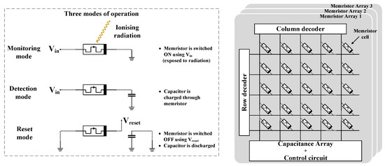
Figure 8. Illustration of a memristor based radiation sensor and its working principle.
2.8. Variable Capacitor Based Radiation Sensor
Variable capacitors or varactors implemented in CMOS technologies (bulk-CMOS and silicon-on-insulator) are viable alternatives to diode and MOSFET based solutions used for radiation sensing. Similar to these solid-state dosimeters, the capacitor based sensors measure the accumulated dose depending on the ionising effects happening inside the dielectric material. Although MOSFET based dosimeters are very popular in terms of reliability and added features, its DC operation methods are very sensitive to various disturbances—in particular to thermal and flicker noise sources [101]. In comparison, variable capacitor based dosimeters have the capability to overcome the noise limits and accomplish ultra-high sensitivity as they employ AC measurement techniques [102][103]. When exposed to radiation, such a sensor exhibits a change in capacitance-voltage (C-V) characteristics due to trapped charges near the Si/SiO2 interface. Subsequently, it results in a different capacitance value in depletion mode, for a given voltage applied between its terminals. Several studies [104][105][106][107] have been carried out on MOS-cap based structures implemented in bulk-CMOS technologies to research the feasibility of radiation dose measurement.
For a given dose of radiation, the sensitivity of the capacitor based detectors relies on the thickness of the dielectric layer and the trapped charge density near the interface. However, the scaling trend of CMOS technologies makes it difficult for MOS-based capacitors to achieve better sensitivity as the oxide thickness is traded off with capacitance tuning [107]. In recent times, the development of FDSOI technology has enabled the varactors to achieve high sensitivity as well as high capacitance per unit area. In the presence of ionising radiation, the thick buried-oxide (BOX) layer beneath the varactor elements collects the radiation induced charges [102]. The resulting shift in capacitance value is measured using a readout circuit. As illustrated in Figure 9, an LC resonator equipped with the radiation sensing capacitor provides a frequency output and the change of which is proportional to the accumulated dose [103]. FDSOI based radiation sensitive varactors are very effective in low dose measurements with very high sensitivity [108]. The radiation sensors are also investigated as reported in [109] for in vivo dosimetry in radiation cancer therapy.
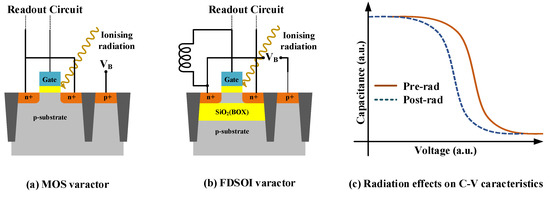
Figure 9. Illustration of (a) MOS varactor, (b) FDSOI varactor based radiation sensor and (c) radiation induced changes in on C-V characteristics.
References
- Rossin, A.D. Dosimetry for Radiation Damage Studies. IEEE Trans. Nucl. Sci. 1964, 11, 130–136.
- Kloepper, R.M. Neutron and Gamma-Ray Rate Sensitivities of Several Dynamic Detectors Used in Radiation Effects. IEEE Trans. Nucl. Sci. 1964, 11, 137–144.
- Beezhold, W.; Beutler, D.; Garth, J.; Griffin, P. A review of the 40-year history of the NSREC’S dosimetry and facilities session (1963–2003). IEEE Trans. Nucl. Sci. 2003, 50, 635–652.
- Hester, D.L.; Glower, D.D.; Overton, L.J. Use of Ferroelectrics for Gamma-Ray Dosimetry. IEEE Trans. Nucl. Sci. 1964, 11, 145–154.
- Birdsall, R.L.; Binder, D.; Peffley, W.M. A Strain Gage Dosimeter for Pulsed Radiation Environment. IEEE Trans. Nucl. Sci. 1968, 15, 346–349.
- Sukis, D.R. Thermoluminescent Properties of CaF2: Dy TLD’S. IEEE Trans. Nucl. Sci. 1971, 18, 185–189.
- Wrobel, T.F.; Berger, R.A. Silicon Calorimeter System for Gamma and Electron-Beam Radiation Dosimetry. IEEE Trans. Nucl. Sci. 1975, 22, 2314–2318.
- Adams, L.; Holmes-Siedle, A. The Development of an MOS Dosimetry Unit for Use in Space. IEEE Trans. Nucl. Sci. 1978, 25, 1607–1612.
- Zoutendyk, J.A.; Malone, C.J. Field Funneling and Range Straggling in Partially Depleted Silicon Surface-Barrier Detectors. IEEE Trans. Nucl. Sci. 1984, 31, 1101–1105.
- Brucker, G.J.; Stassinopoulos, E.G.; Van Gunten, O.; August, L.S.; Jordan, T.M. The Damage Equivalence of Electrons, Protons, and Gamma Rays in MOS Devices. IEEE Trans. Nucl. Sci. 1982, 29, 1966–1969.
- Stapor, W.J.; August, L.S.; Wilson, D.H.; Oldham, T.R.; Murray, K.M. Proton and Heavy-Ion Radiation Damage Studies in MOS Transistors. IEEE Trans. Nucl. Sci. 1985, 32, 4399–4404.
- Rosenfeld, A.; Carolan, M.; Kaplan, G.; Allen, B.; Khivrich, V. MOSFET dosimeters: The role of encapsulation on dosimetric characteristics in mixed gamma-neutron and megavoltage X-ray fields. IEEE Trans. Nucl. Sci. 1995, 42, 1870–1877.
- O’Connell, B.; Conneely, C.; McCarthy, C.; Doyle, J.; Lane, W.; Adams, L. Electrical performance and radiation sensitivity of stacked PMOS dosimeters under bulkbias control. IEEE Trans. Nucl. Sci. 1998, 45, 2689–2694.
- Scheick, L.; McNulty, P.; Roth, D. Dosimetry based on the erasure of floating gates in the natural radiation environments in space. IEEE Trans. Nucl. Sci. 1998, 45, 2681–2688.
- Martin, M.; Roth, D.; Garrison-Darrin, A.; McNulty, P.; Andreou, A. FGMOS dosimetry: Design and implementation. IEEE Trans. Nucl. Sci. 2001, 48, 2050–2055.
- Zoutendyk, J.A.; Malone, C.J.; Smith, L.S. Experimental Determination of Single-Event Upset (SEU) as a Function of Collected Charge in Bipolar Integrated Circuits. IEEE Trans. Nucl. Sci. 1984, 31, 1167–1174.
- Farrell, G.E.; McNulty, P.J. Microdosimetric Aspects of Proton-Induced Nuclear Reactions in Thin Layers of Silicon. IEEE Trans. Nucl. Sci. 1982, 29, 2012–2016.
- Rosenfeld, A. MOSFET Dosimetry on Modern Radiation Oncology Modalities. Radiat. Prot. Dosim. 2002, 101, 393–398.
- Fleetwood, D.M. Radiation Effects in a Post-Moore World. IEEE Trans. Nucl. Sci. 2021, 68, 509–545.
- Benedetto, J.M.; Boesch, H.E.; McLean, F.B.; Mize, J.P. Hole Removal in Thin-Gate MOSFETs by Tunneling. IEEE Trans. Nucl. Sci. 1985, 32, 3916–3920.
- Saks, N.S.; Ancona, M.G.; Modolo, J.A. Generation of Interface States by Ionizing Radiation in Very Thin MOS Oxides. IEEE Trans. Nucl. Sci. 1986, 33, 1185–1190.
- Dodd, P.E.; Shaneyfelt, M.R.; Schwank, J.R.; Felix, J.A. Current and Future Challenges in Radiation Effects on CMOS Electronics. IEEE Trans. Nucl. Sci. 2010, 57, 1747–1763.
- Dodd, P.; Shaneyfelt, M.; Felix, J.; Schwank, J. Production and propagation of single-event transients in high-speed digital logic ICs. IEEE Trans. Nucl. Sci. 2004, 51, 3278–3284.
- Kasahara, S.; Mitani, T.; Ogasawara, K.; Takashima, T.; Hirahara, M.; Asamura, K. Application of single-sided silicon strip detector to energy and charge state measurements of medium energy ions in space. Nucl. Instrum. Methods Phys. Res. Sect. Accel. Spectrometers Detect. Assoc. Equip. 2009, 603, 355–360.
- Havranek, M.; Benka, T.; Hejtmanek, M.; Janoska, Z.; Kafka, V.; Kopecek, J.; Kuklova, M.; Marcisovska, M.; Marcisovsky, M.; Neue, G.; et al. MAPS sensor for radiation imaging designed in 180 nm SOI CMOS technology. J. Instrum. 2018, 13, C06004.
- Wong, W.; Alozy, J.; Ballabriga, R.; Campbell, M.; Kremastiotis, I.; Llopart, X.; Poikela, T.; Sriskaran, V.; Tlustos, L.; Turecek, D. Introducing Timepix2, a frame-based pixel detector readout ASIC measuring energy deposition and arrival time. Radiat. Meas. 2020, 131, 106230.
- Ravotti, F. Dosimetry Techniques and Radiation Test Facilities for Total Ionizing Dose Testing. IEEE Trans. Nucl. Sci. 2018, 65, 1440–1464.
- Damulira, E.; Yusoff, M.N.S.; Omar, A.F.; Mohd Taib, N.H. A review: Photonic devices used for dosimetry in medical radiation. Sensors 2019, 19, 2226.
- Zhang, L.H.; Platt, S.P.; Edwards, R.; Allabush, C. In-situ neutron dosimetry for single-event effect accelerated testing. IEEE Trans. Nucl. Sci. 2009, 56, 2070–2076.
- Duan, Y.; Yao, Y.; Li, Z.; Zhou, J.; Huang, P.; Gao, W. SENSROC12: A Four-Channel Binary-Output Front-End Readout ASIC for Si-PIN-Based Personal Dosimeters. IEEE Trans. Nucl. Sci. 2019, 66, 1976–1983.
- Becker, H.N.; Farr, W.H.; Zhu, D.Q. Radiation Response of Emerging High Gain, Low Noise Detectors. IEEE Trans. Nucl. Sci. 2007, 54, 1129–1135.
- Bertuccio, G.; Puglisi, D.; Macera, D.; Di Liberto, R.; Lamborizio, M.; Mantovani, L. Silicon carbide detectors for in vivo dosimetry. IEEE Trans. Nucl. Sci. 2014, 61, 961–966.
- Chen, X.J.; Johnson, E.B.; Staples, C.J.; Chapman, E.; Alberghini, G.; Benton, E.; Christian, J.F. Space Dosimeters Based on CMOS SSPM Technology. IEEE Trans. Nucl. Sci. 2010, 57, 3450–3455.
- Chen, X.J.; Johnson, E.B.; Stapels, C.J.; Fernandez, D.; Podolsky, M.; Vogel, S.; Christian, J.F. Effects of Proton Radiation on Noise Performance in Solid-State Photomultipliers. IEEE Trans. Nucl. Sci. 2016, 63, 1109–1116.
- Barnaby, H.J. Total-Ionizing-Dose Effects in Modern CMOS Technologies. IEEE Trans. Nucl. Sci. 2006, 53, 3103–3121.
- McGarrity, J.M. Considerations for Hardening MOS Devices and Circuits for Low Radiation Doses. IEEE Trans. Nucl. Sci. 1980, 27, 1739–1744.
- Holmes-Siedle, A.; Adams, L.; Leffler, J.S.; Lindgren, S.R. The RADFET system for real-time dosimeter in nuclear facility. IEEE Trans. Nucl. Sci. 1983, 26, 025004.
- RADFET: A review of the use of metaloxide-silicon devices as integrating dosimeters. Int. J. Radiat. Appl. Instrum. Part C Radiat. Phys. Chem. 1986, 28, 235–244.
- Butson, M.J.; Rozenfeld, A.; Mathur, J.N.; Carolan, M.; Wong, T.P.; Metcalfe, P.E. A new radiotherapy surface dose detector: The MOSFET. Med. Phys. 1996, 23, 655–658.
- Peet, D.; Pryor, M. Evaluation of a MOSFET radiation sensor for the measurement of entrance surface dose in diagnostic radiology. Br. J. Radiol. 1999, 72, 562–568.
- Sarrabayrouse, G.; Siskos, S. Radiation dose measurment using MOSFETs. IEEE Instrum. Meas. Mag. 1998, 1, 26–34.
- Lipovetzky, J.; García-Inza, M.A.; Carbonetto, S.; Carra, M.J.; Redin, E.; Sambuco Salomone, L.; Faigon, A. Field Oxide n-channel MOS Dosimeters Fabricated in CMOS Processes. IEEE Trans. Nucl. Sci. 2013, 60, 4683–4691.
- Haran, A.; Jaksic, A.; Refaeli, N.; Eliyahu, A.; David, D.; Barak, J. Temperature effects and long term fading of implanted and unimplanted gate oxide RADFETs. IEEE Trans. Nucl. Sci. 2004, 51, 2917–2921.
- Garcia-Inza, M.; Carbonetto, S.; Lipovetzky, J.; Carra, M.J.; Salomone, L.S.; Redin, E.G.; Faigon, A. Switched Bias Differential MOSFET Dosimeter. IEEE Trans. Nucl. Sci. 2014, 61, 1407–1413.
- Carbonetto, S.; Garcia-Inza, M.; Lipovetzky, J.; Carra, M.J.; Redin, E.; Salomone, L.S.; Faigón, A. CMOS Differential and Amplified Dosimeter with Field Oxide N-Channel MOSFETs. IEEE Trans. Nucl. Sci. 2014, 61, 3466–3471.
- Kassabov, J.; Nedev, N.; Smirnov, N. Radiation dosimeter based on floating gate MOS transistor. Radiat. Eff. Defects Solids 1991, 116, 155–158.
- Tarr, N.; Mackay, G.; Shortt, K.; Thomson, I. A floating gate MOSFET dosimeter requiring no external bias supply. In Proceedings of the RADECS 97, Fourth European Conference on Radiation and its Effects on Components and Systems (Cat. No.97TH8294), Cannes, France, 15–19 September 1997; pp. 277–281.
- Tarr, N.; Shortt, K.; Wang, Y.; Thomson, I. A sensitive, temperature-compensated, zero-bias floating gate MOSFET dosimeter. IEEE Trans. Nucl. Sci. 2004, 51, 1277–1282.
- Garcia-Moreno, E.; Isern, E.; Roca, M.; Picos, R.; Font, J.; Cesari, J.; Pineda, A. Floating Gate CMOS Dosimeter With Frequency Output. IEEE Trans. Nucl. Sci. 2012, 59, 373–378.
- Chatterjee, B.; Mousoulis, C.; Seo, D.H.; Kumar, A.; Maity, S.; Scott, S.M.; Valentino, D.J.; Morisette, D.T.; Peroulis, D.; Sen, S. A Wearable Real-Time CMOS Dosimeter With Integrated Zero-Bias Floating Gate Sensor and an 861-nW 18-Bit Energy-Resolution Scalable Time-Based Radiation to Digital Converter. IEEE J. Solid-State Circ. 2020, 55, 650–665.
- Pikhay, E.; Roizin, Y.; Nemirovsky, Y. Ultra-low power consuming direct radiation sensors based on floating gate structures. J. Low Power Electron. Appl. 2017, 7, 20.
- Garcia-Moreno, E.; Isern, E.; Roca, M.; Picos, R.; Font, J.; Cesari, J.; Pineda, A. Temperature Compensated Floating Gate MOS Radiation Sensor With Current Output. IEEE Trans. Nucl. Sci. 2013, 60, 4026–4030.
- Brucoli, M.; Danzeca, S.; Brugger, M.; Masi, A.; Pineda, A.; Cesari, J.; Dusseau, L.; Wrobel, F. Floating Gate Dosimeter Suitability for Accelerator-Like Environments. IEEE Trans. Nucl. Sci. 2017, 64, 2054–2060.
- Brucoli, M.; Cesari, J.; Danzeca, S.; Brugger, M.; Masi, A.; Pineda, A.; Dusseau, L.; Wrobel, F. Investigation on Passive and Autonomous Mode Operation of Floating Gate Dosimeters. IEEE Trans. Nucl. Sci. 2019, 66, 1620–1627.
- Prinzie, J.; Thys, S.; Van Bockel, B.; Wang, J.; De Smedt, V.; Leroux, P. An SRAM-Based Radiation Monitor With Dynamic Voltage Control in 0.18-μm CMOS Technology. IEEE Trans. Nucl. Sci. 2019, 66, 282–289.
- Harboe-Sorensen, R.; Guerre, F.X.; Roseng, A. Design, Testing and Calibration of a “Reference SEU Monitor” System. In Proceedings of the 2005 8th European Conference on Radiation and Its Effects on Components and Systems, Cap d’Agde, France, 19–23 September 2005; pp. 3–7.
- Spiezia, G.; Peronnard, P.; Masi, A.; Brugger, M.; Brucoli, M.; Danzeca, S.; Alia, R.G.; Losito, R.; Mekki, J.; Oser, P.; et al. A New RadMon Version for the LHC and its Injection Lines. IEEE Trans. Nucl. Sci. 2014, 61, 3424–3431.
- Harboe-Sorensen, R.; Poivey, C.; Fleurinck, N.; Puimege, K.; Zadeh, A.; Guerre, F.X.; Lochon, F.; Kaddour, M.; Li, L.; Walter, D.; et al. The Technology Demonstration Module On-Board PROBA-II. IEEE Trans. Nucl. Sci. 2011, 58, 1001–1007.
- Blackmore, E.; Trinczek, M.; Jiang, K.; Sachdev, M.; Wright, D. SRAM Dosimeter for Characterizing the TRIUMF Proton and Neutron Beams. IEEE Trans. Nucl. Sci. 2019, 66, 276–281.
- Tsiligiannis, G.; Danzeca, S.; García Alía, R.; Infantino, A.; Lesea, A.; Brugger, M.; Masi, A.; Gilardoni, S.; Saigné, F. Radiation Effects on Deep Submicrometer SRAM-Based FPGAs Under the CERN Mixed-Field Radiation Environment. IEEE Trans. Nucl. Sci. 2018, 65, 1511–1518.
- Alía, R.G.; Tali, M.; Brugger, M.; Cecchetto, M.; Cerutti, F.; Cononetti, A.; Danzeca, S.; Esposito, L.; Fernández-Martínez, P.; Gilardoni, S.; et al. Direct Ionization Impact on Accelerator Mixed-Field Soft-Error Rate. IEEE Trans. Nucl. Sci. 2020, 67, 345–352.
- Kramer, D.; Brugger, M.; Klupak, V.; Pignard, C.; Roeed, K.; Spiezia, G.; Viererbl, L.; Wijnands, T. LHC RadMon SRAM Detectors Used at Different Voltages to Determine the Thermal Neutron to High Energy Hadron Fluence Ratio. IEEE Trans. Nucl. Sci. 2011, 58, 1117–1122.
- Wang, J.; Prinzie, J.; Coronetti, A.; Thys, S.; Alia, R.G.; Leroux, P. Study of SEU Sensitivity of SRAM-Based Radiation Monitors in 65-nm CMOS. IEEE Trans. Nucl. Sci. 2021, 68, 913–920.
- Secondo, R.; Foucard, G.; Danzeca, S.; Losito, R.; Peronnard, P.; Masi, A.; Brugger, M.; Dusseau, L. Embedded Detection and Correction of SEU Bursts in SRAM Memories Used as Radiation Detectors. IEEE Trans. Nucl. Sci. 2016, 63, 2168–2175.
- Meershoek, R.; Verhelst, B.; McInerney, R.; Thijssen, L. Functional and I/sub DDQ/ testing on a static RAM. Proc. Int. Test Conf. 1990, 1990, 929–937.
- Kuo, C.; Toms, T.; Neel, B.; Jelemensky, J.; Carter, E.; Smith, P. Soft-defect detection (SDD) technique for a high-reliability CMOS SRAM. IEEE J. Solid-State Circ. 1990, 25, 61–67.
- Naik, S.; Agricola, F.; Maly, W. Failure analysis of high-density CMOS SRAMs: Using realistic defect modeling and I/sub DDQ/ testing. IEEE Des. Test Comput. 1993, 10, 13–23.
- Su, S.T.; Makki, R.Z. Testing of Static Random Access Memories by Monitoring Dynamic Power Supply Current. J. Electron. Test. 1992, 3, 265–278.
- Yokoyama, H.; Tamamoto, H.; Narita, Y. A current testing for CMOS static RAMs. In Proceedings of the Records of the 1993 IEEE International Workshop on Memory Testing, San Jose, CA, USA, 9–10 August 1993; pp. 137–142.
- Lo, J.C.; Daly, J.; Nicolaidis, M. Design of static CMOS self-checking circuits using built-in current sensing. In Proceedings of the Digest of Papers: FTCS-22: The Twenty-Second International Symposium on Fault-Tolerant Computing, Boston, MA, USA, 8–10 July 1992; pp. 104–111.
- Nicolaidis, M.; Vargas, F.; Courtois, B. Design of built-in current sensors for concurrent checking in radiation environments. IEEE Trans. Nucl. Sci. 1993, 40, 1584–1590.
- Neto, E.; Ribeiro, I.; Vieira, M.; Wirth, G.; Kastensmidt, F. Using Bulk Built-in Current Sensors to Detect Soft Errors. IEEE Micro 2006, 26, 10–18.
- Ndai, P.; Agarwal, A.; Chen, Q.; Roy, K. A soft error monitor using switching current detection. In Proceedings of the 2005 International Conference on Computer Design, San Jose, CA, USA, 2–5 October 2005; pp. 185–190.
- Bastos, R.P.; Natale, G.D.; Flottes, M.L.; Rouzeyre, B. A New Bulk Built-In Current Sensor-Based Strategy for Dealing with Long-Duration Transient Faults in Deep-Submicron Technologies. In Proceedings of the 2011 IEEE International Symposium on Defect and Fault Tolerance in VLSI and Nanotechnology Systems, Vancouver, BC, Canada, 3–5 October 2011; pp. 302–308.
- Simionovski, A.; Wirth, G.I. A Bulk Built-in Current Sensor for SET detection with dynamic memory cell. In Proceedings of the 2012 IEEE 3rd Latin American Symposium on Circuits and Systems (LASCAS), Playa del Carmen, Mexico, 29 February–2 March 2012; pp. 1–4.
- Bastos, R.P.; Torres, F.S.; Dutertre, J.M.; Flottes, M.L.; Di Natale, G.; Rouzeyre, B. A bulk built-in sensor for detection of fault attacks. In Proceedings of the 2013 IEEE International Symposium on Hardware-Oriented Security and Trust (HOST), Austin, TX, USA, 2–3 June 2013; pp. 51–54.
- Zhang, Z.; Ren, Y.; Chen, L.; Gaspard, N.J.; Witulski, A.F.; Holman, T.W.; Bhuva, B.L.; Wen, S.J.; Sammynaiken, R. A bulk built-in voltage sensor to detect physical location of single-event transients. J. Electron. Test. 2013, 29, 249–253.
- Simionovski, A.; Vaz, R.G.; Gonçalez, O.L.; Wirth, G. Impact of total ionizing dose on bulk built-in current sensors with dynamic storage cell. J. Electron. Test. 2015, 31, 411–417.
- Dutertre, J.; Possamai Bastos, R.; Potin, O.; Flottes, M.; Rouzeyre, B.; Di Natale, G.; Sarafianos, A. Improving the ability of Bulk Built-In Current Sensors to detect Single Event Effects by using triple-well CMOS. Microelectron. Reliab. 2014, 54, 2289–2294.
- Cappelletti, P. Non volatile memory evolution and revolution. In Proceedings of the 2015 IEEE International Electron Devices Meeting (IEDM), Washington, DC, USA, 7–9 December 2015; pp. 10.1.1–10.1.4.
- Monzio Compagnoni, C.; Goda, A.; Spinelli, A.S.; Feeley, P.; Lacaita, A.L.; Visconti, A. Reviewing the Evolution of the NAND Flash Technology. Proc. IEEE 2017, 105, 1609–1633.
- Fabiano, M.; Furano, G. NAND flash storage technology for mission-critical space applications. IEEE Aerosp. Electron. Syst. Mag. 2013, 28, 30–36.
- Furano, G.; Meoni, G.; Dunne, A.; Moloney, D.; Ferlet-Cavrois, V.; Tavoularis, A.; Byrne, J.; Buckley, L.; Psarakis, M.; Voss, K.O.; et al. Towards the Use of Artificial Intelligence on the Edge in Space Systems: Challenges and Opportunities. IEEE Aerosp. Electron. Syst. Mag. 2020, 35, 44–56.
- Li, P.; Dang, W.; Qin, T.; Zhang, Z.; Lv, C. A Competing Risk Model of Reliability Analysis for NAND-Based SSDs in Space Application. IEEE Access 2019, 7, 23430–23441.
- Alvarez, M.; Hernando, C.; Cesari, J.; Pineda, A.; Garcia-Moreno, E. Total Ionizing Dose Characterization of a Prototype Floating Gate MOSFET Dosimeter for Space Applications. IEEE Trans. Nucl. Sci. 2013, 60, 4281–4288.
- Oldham, T.R.; Ladbury, R.L.; Friendlich, M.; Kim, H.S.; Berg, M.D.; Irwin, T.L.; Seidleck, C.; LaBel, K.A. SEE and TID Characterization of an Advanced Commercial 2Gbit NAND Flash Nonvolatile Memory. IEEE Trans. Nucl. Sci. 2006, 53, 3217–3222.
- Irom, F.; Nguyen, D.N.; Underwood, M.L.; Virtanen, A. Effects of Scaling in SEE and TID Response of High Density NAND Flash Memories. IEEE Trans. Nucl. Sci. 2010, 57, 3329–3335.
- Gerardin, S.; Bagatin, M.; Paccagnella, A.; Ferlet-Cavrois, V.; Visconti, A.; Frost, C.D. Neutron and Alpha Single Event Upsets in Advanced NAND Flash Memories. IEEE Trans. Nucl. Sci. 2014, 61, 1799–1805.
- Bagatin, M.; Gerardin, S.; Paccagnella, A.; Beltrami, S.; Camerlenghi, E.; Bertuccio, M.; Costantino, A.; Zadeh, A.; Ferlet-Cavrois, V.; Santin, G.; et al. Effects of Heavy-Ion Irradiation on Vertical 3-D NAND Flash Memories. IEEE Trans. Nucl. Sci. 2018, 65, 318–325.
- Chen, D.; Wilcox, E.; Ladbury, R.L.; Seidleck, C.; Kim, H.; Phan, A.; LaBel, K.A. Heavy Ion and Proton-Induced Single Event Upset Characteristics of a 3-D NAND Flash Memory. IEEE Trans. Nucl. Sci. 2018, 65, 19–26.
- Bagatin, M.; Gerardin, S.; Paccagnella, A.; Beltrami, S.; Cazzaniga, C.; Frost, C.D. Atmospheric Neutron Soft Errors in 3-D NAND Flash Memories. IEEE Trans. Nucl. Sci. 2019, 66, 1361–1367.
- Bagatin, M.; Gerardin, S.; Paccagnella, A.; Beltrami, S.; Costantino, A.; Poivey, C.; Santin, G.; Ferlet-Cavrois, V.; Cazzaniga, C.; Frost, C. A Heavy-Ion Detector Based on 3-D NAND Flash Memories. IEEE Trans. Nucl. Sci. 2020, 67, 154–160.
- Bagatin, M.; Gerardin, S.; Paccagnella, A.; Beltrami, S. Depth Dependence of Threshold Voltage Shift in 3-D Flash Memories Exposed to X-rays. IEEE Trans. Nucl. Sci. 2021, 68, 659–664.
- Andjelkovic, M.; Chen, J.; Simevski, A.; Stamenkovic, Z.; Krstic, M.; Kraemer, R. A Review of Particle Detectors for Space-Borne Self-Adaptive Fault-Tolerant Systems. In Proceedings of the 2020 IEEE East-West Design Test Symposium (EWDTS), Varna, Bulgaria, 4–7 September 2020; pp. 1–8.
- Boukhobza, J.; Olivier, P. 10-Emerging Non-volatile Memories. In Flash Memory Integration; Boukhobza, J., Olivier, P., Eds.; Elsevier: Amsterdam, The Netherlands, 2017; pp. 203–224.
- Carrara, S. The Birth of a New Field: Memristive Sensors. A Review. IEEE Sens. J. 2021, 21, 12370–12378.
- Barnaby, H.J.; Malley, S.; Land, M.; Charnicki, S.; Kathuria, A.; Wilkens, B.; DeIonno, E.; Tong, W.M. Impact of Alpha Particles on the Electrical Characteristics of TiO2 Memristors. IEEE Trans. Nucl. Sci. 2011, 58, 2838–2844.
- Marinella, M.J.; Dalton, S.M.; Mickel, P.R.; Dodd, P.E.D.; Shaneyfelt, M.R.; Bielejec, E.; Vizkelethy, G.; Kotula, P.G. Initial Assessment of the Effects of Radiation on the Electrical Characteristics of TaOx Memristive Memories. IEEE Trans. Nucl. Sci. 2012, 59, 2987–2994.
- Yuan, F.; Zhang, Z.; Wang, J.C.; Pan, L.; Xu, J.; Lai, C.S. Total ionizing dose (TID) effects of γ ray radiation on switching behaviors of Ag/AlOx/Pt RRAM device. Nanoscale Res. Lett. 2014, 9, 452.
- Abunahla, H.; Mohammad, B.; Mahmoud, L.; Darweesh, M.; Alhawari, M.; Jaoude, M.A.; Hitt, G.W. MemSens: Memristor-Based Radiation Sensor. IEEE Sens. J. 2018, 18, 3198–3205.
- Fleetwood, D.; Meisenheimer, T.; Scofield, J. 1/f noise and radiation effects in MOS devices. IEEE Trans. Electron Devices 1994, 41, 1953–1964.
- Li, Y.; Porter, W.M.; Ma, R.; Reynolds, M.A.; Gerbi, B.J.; Koester, S.J. Capacitance-Based Dosimetry of Co-60 Radiation Using Fully-Depleted Silicon-on-Insulator Devices. IEEE Trans. Nucl. Sci. 2015, 62, 3012–3019.
- Li, Y.; Chaganti, V.R.S.K.; Reynolds, M.A.; Gerbi, B.J.; Koester, S.J. Demonstration of a Passive Wireless Radiation Detector Using Fully-Depleted Silicon-on-Insulator Variable Capacitors. IEEE Trans. Nucl. Sci. 2017, 64, 544–549.
- Gopalan, M.S. Experimental Study of MOS Capacitors as Wireless Radiation Dose Sensors; Arizona State University: Tempe, AZ, USA, 2010.
- Scott, S.; Mousoulis, C.; Raghunathan, N.; Peroulis, D.; Valentino, D.J.; Walerow, P.A.; Salasky, M.; Rajabather, H.; Thistlethwaite, J.; McNamee, T. MOS-capacitor-based ionizing radiation sensors for occupational dosimetry applications. In Proceedings of the 2015 IEEE SENSORS, Busan, Korea, 1–4 November 2015; pp. 1–4.
- Mousoulis, C.; Elmiger, C.; Singhal, M.; Xuan, Y.; McNamee, T.; Thistlethwaite, J.; Walerow, P.A.; Salasky, M.; Scott, S.; Valentino, D.J.; et al. Characterization of fading of a MOS-based sensor for occupational radiation dosimetry. In Proceedings of the 2016 IEEE SENSORS, Orlando, FL, USA, 30 October–3 November 2016; pp. 1–3.
- Xuan, Y.; Mousoulis, C.; Kumar, A.; Elmiger, C.I.; Scott, S.; Valentino, D.J.; Peroulis, D. 3D MOS-capacitor-based ionizing radiation sensors. In Proceedings of the 2017 IEEE SENSORS, Glasgow, UK, 29 October–1 November 2017; pp. 1–3.
- Vaidhyanathan, G.; Koester, S.J. High-Q FDSOI varactors for wireless radiation sensing. In Proceedings of the IEEE 2011 International SOI Conference, Tempe, AZ, USA, 3–6 October 2011; pp. 1–2.
- Li, Y.; Porter, W.M.; Kshirsagar, C.; Roth, I.; Su, Y.; Reynolds, M.A.; Gerbi, B.J.; Koester, S.J. Fully-Depleted Silicon-on-Insulator Devices for Radiation Dosimetry in Cancer Therapy. IEEE Trans. Nucl. Sci. 2014, 61, 3443–3450.