Your browser does not fully support modern features. Please upgrade for a smoother experience.
Submitted Successfully!
 +1 credit
Thank you for your contribution! You can also upload a video entry or images related to this topic.
For video creation, please contact our Academic Video Service.
Video Upload Options
We provide professional Academic Video Service to translate complex research into visually appealing presentations. Would you like to try it?
Cite
If you have any further questions, please contact Encyclopedia Editorial Office.
Chen, J. ZnO Nanowires Cold Cathode. Encyclopedia. Available online: https://encyclopedia.pub/entry/13910 (accessed on 26 June 2026).
Chen J. ZnO Nanowires Cold Cathode. Encyclopedia. Available at: https://encyclopedia.pub/entry/13910. Accessed June 26, 2026.
Chen, Jun. "ZnO Nanowires Cold Cathode" Encyclopedia, https://encyclopedia.pub/entry/13910 (accessed June 26, 2026).
Chen, J. (2021, September 06). ZnO Nanowires Cold Cathode. In Encyclopedia. https://encyclopedia.pub/entry/13910
Chen, Jun. "ZnO Nanowires Cold Cathode." Encyclopedia. Web. 06 September, 2021.
Copy Citation
A cold cathode has many applications in high frequency and high power electronic devices, X-ray source, vacuum microelectronic devices and vacuum nanoelectronic devices. After decades of exploration on the cold cathode materials, ZnO nanowire has been regarded as one of the most promising candidates, in particular for large area field emitter arrays (FEAs). Numerous works on the fundamental field emission properties of ZnO nanowire, as well as demonstrations of varieties of large area vacuum microelectronic applications, have been reported. Moreover, techniques such as modifying the geometrical structure, surface decoration and element doping were also proposed for optimizing the field emissions.
ZnO nanowire
field emission
flat panel vacuum microelectronic applications
1. Introduction
When a strong field is applied on a cathode surface, its vacuum barrier will bend. If the barrier width for an electron is as narrow as several nanometers, there is a considerable probability the electrons will tunnel into the vacuum. This process is referred to as field electron emission. Field electron emission is the basic principle of a cold cathode. Compared to a traditional thermionic cathode, a cold cathode has many advantages, such as fast response time, low power consumption, narrow energy spread, compact size, high brightness, etc. One of the most attractive features of a cold cathode is probably its capability in miniaturized and addressable devices, which creates the concept of field emitter arrays (FEAs) that has potential applications in field emission display (FED) [1], parallel electron beam (e-beam) lithography [2], flat panel X-ray source [3]and large area photodetectors[4].
2. Applications
The foremost motivation for the research on FEAs is probably to apply them in the flat panel field-emission display. Since other display techniques such as LCD, OLED and quantum dots have been chosen by the industry in recent years, this attempt has faded away and been transferred to the applications of flat panel light source, X-ray source and photodetector. In this section, the progress of the above applications based on ZnO nanowires cold cathode will be introduced in detail.
2.1. Field Emission Display (FED)
Generally, there are two kinds of device structure that can realize field emitters with addressable function as required for FED. One is a diode structure whereby both the anode and cathode have electrode strips perpendicular to each other, the schematic diagram of which is shown in Figure 1a. When a high voltage is applied between one anode electrode strip and one cathode electrode strip, field emitters on the overlap region between the two electrodes can emit electrons, which works as one pixel of the device. By screen printing ZnO nanotetrapers on the cathode electrode of this kind of device structure, K. Zheng et al. [5] demonstrated the display of some Chinese characters as shown in Figure 1b. Another is a triode structure that consists of a phosphor-coated glass anode and the addressable gated FEAs, a typical gated structure of which fabricated by Y. Li et al. [6] can be seen in Figure 2a–d. In this device, the anode is applied with a fixed anode voltage. When a voltage is applied between the gate and cathode electrodes, the nanowires in the corresponding pixel can emit electrons. The display of full screen, cartoon image and some Chinese characters are demonstrated from the device, which are shown in Figure 2e–j.
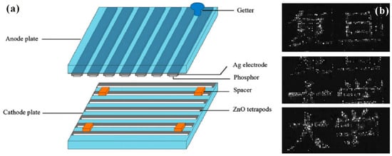
Figure 1. Demonstration of a diode structured field-emission display device based on ZnO nanotetrapods. (a) Device structure. (b) Some Chinese characters displayed by the device. Reproduced from [5], with the permission of Elsevier, 2008.
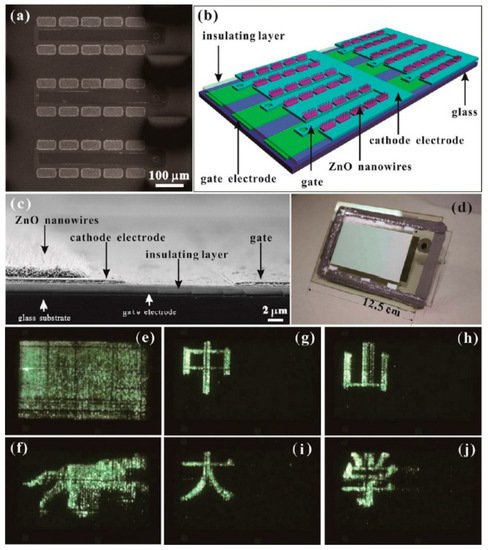
Figure 2. Demonstration of an addressable field emission device based on ZnO nanowires. Top view SEM image (a), schematic diagram (b), cross-sectional SEM image (c) and optical image (d) of the device. Full screen (e), cartoon of a running dog (f) and some Chinese characters (g–j) displayed by the device. Reproduced from [6], with the permission of ACS Publications, 2017.
To further meet the requirements of high-resolution device application, a focusing gate structure is needed for overcoming the problem of electron beam divergence. In view of this, Y. Liu et al.[7] demonstrated the ZnO nanowire FEAs with line-addressing and focusing capability. By changing the focusing gate voltage from 50 to −50 V, the linewidth of one row of the field-emission pattern can be reduced from 2.25 mm to 1.35 mm under a distance of 5 mm between the anode and cathode. X. Cao et al. further upgraded this device with fully addressing capability by using a via structure, the schematic diagram of which can be seen in Figure 3a,b. The addressing capability of the device has been demonstrated by displaying some English characters as shown in Figure 3c, while the focusing ability still remains which can be seen in Figure 3d.
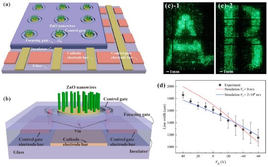
Figure 3. Demonstration of an addressable gated field-emission device with focusing gate based on ZnO nanowires. Schematic diagram for multi (a) and one (b) pixel of the device structure. English characters of “A” (c-1) and “B” (c-2) displayed by the device. (d) The relationship between the line width on the phosphor anode of one row pixels and the focusing gate voltage. Reproduced from [8], with the permission of IEEE, 2019.
It should be pointed out that although FED no longer wins favor in the market of flat-panel displays, the techniques for field emitter arrays are still important for other flat-panel devices, such as UV illumination, X-ray source, e-beam lithography and photodetector, which are at their preliminary development stage.
2.2. Illumination
The principle for the field-emission light source is nearly the same as that for FED, which utilizes high-energy electrons to bombard the phosphor coated anode and produces cathodoluminescence. By contrast with the FED device, the addressable FEAs are not required for a light source, which makes it easier to be fabricated. For example, Y. Chen et al. [9] fabricated a triode structure field-emission light source based on ZnO nanotetrapods, the device structure of which can be seen schematically in Figure 4a. The gated controlled capability was demonstrated from the field-emission images recorded at different gate voltage (Figure 4b–e). By applying the anode voltage of 3300 V and gate voltage of 200 V, a luminous intensity of 8000 cd/m2 can be obtained from that device. Moreover, a diagonal 10-inch field emission light source with a diode structure is also fabricated by using ZnO nanowires [10].
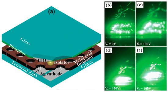
Figure 4. Demonstration of a field-emission light source based on ZnO nanostructures. (a) Schematic diagram of the device. (b–e) Field-emission images for gate voltage of 0, 100, 150 and 200 V. Reproduced from [9], with the permission of RSC Pub, 2014.
In addition to the visible light source, FEAs can also be utilized to generate the UV light by using the wide bandgap semiconductor as the anode. A field-emission UV source can avoid the problem of a solid-stated UV-LED that requires both n-type and p-type semiconductors for the radiation. This is because for some materials, e.g., ZnO, it is not so easy to realize stable doping of p-type impurities. A demonstration of a ZnO nanowires-based UV source has been reported by J. Yin et al. [11], the schematic diagram of the diode structure device of which is shown in Figure 5a. The field emission I-V characteristics and uniform field emission pattern of the device can be seen in Figure 5b–d. By using the polycrystalline Ga2O3 as the anode, the cathodoluminescent spectrum with peaks around 400 nm has been achieved, which is shown in Figure 5e.
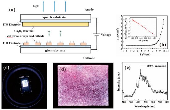
Figure 5. Demonstration of an ultraviolet (UV) light source based on ZnO nanowires cold cathode. (a) Schematic diagram of the device. (b) Field-emission characteristics. (c) Optical image of the operating device. (d) Emission pattern. (e) Cathodoluminescent spectrum. Reproduced from [11], with the permission of IEEE, 2020.
2.3. Flat Panel X-ray Source
The flat panel X-ray source can be the next research spot to substitute the FED, because of the increasing demand for portable and low-cost medical X-ray computerized tomography (CT). Although the basic principle of this device is to use a metal target to replace the phosphor coated glass in the FED, a much higher anode voltage is needed for generating the X-ray radiation. On the other hand, whether the nanowire field emitter can sustain the X-ray irradiation is important for fabricating a reliable device. D. Chen et al. [12] first demonstrated a transmission-type flat-panel X-ray source using ZnO nanowires, the schematic diagram and optical image of which can be seen in Figure 6a,b. The X-ray energy spectra and the X-ray projected images of metal mesh with different linewidth can be seen in Figure 6c–e. Subsequently, a double-sided irradiating flat-panel X-ray source using ZnO nanowires was also demonstrated by their group [13], which utilized both the transmission and reflection of X-rays with ~200 mGy/min dose rate. Another flat-panel X-ray source has also been fabricated by using In-doped ZnO nanowires [14].
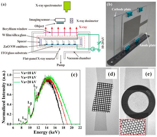
Figure 6. Flat-panel X-ray source based on ZnO nanowires. (a) Schematic diagram for the device structure. (b) Optical image of the device. (c) X-ray energy spectra. X-ray image of a metal mesh with linewidth of 200 μm (d) and 25 μm (e). Reproduced from [12], with the permission of AIP Publishing, 2015.
Since the major advantage of a flat-panel X-ray source is its addressing capability, the ultimate goal for the research of flat-panel X-ray sources is to realize an addressable device. A successful demonstration of a fully vacuum-sealed addressable flat panel X-ray source based on ZnO nanowire FEAs has been reported recently by X. Cao et al. [15], the schematic diagram and optical image of which can be seen in Figure 7a,b. Although the X-ray image of the integrated circuit chips as shown in Figure 7c is blurred due to the low dose rate of ~200 nGy/s, their work opens up the possibility for realizing the functional addressable flat panel X-ray source, which could lead to a revolution in medical radiotherapy or CT systems.
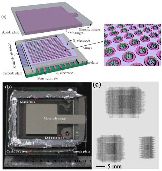
Figure 7. Addressable flat panel X-ray source based on ZnO nanowires. Schematic diagram (a) and optical image (b) of the device. (c) X-ray image of the integrated circuit chips. Reproduced from [16], with the permission of AIP Publishing, 2021.
Considering that the flat panel X-ray source has a larger radiant area than that of the usual X-ray tube, their performances in projection imaging should be different. To obtain a better understanding, L. Wang et al. [17] characterized the spatial resolution of a diagonal 4-inch flat panel X-ray source based on a ZnO nanowires cold cathode. Using the line-pair testing card, they obtained a contrast of more than 5 lp/mm (Figure 8a). To further investigate the dependence of object position on the resolution, they also used a modulation transfer function (MTF) analysis method to characterize the imaging spatial resolution, the measurement setup of which can be seen schematically in Figure 8b. The monotonic decrease and increased dependences of the distance between object and detector (z) and the distance between X-ray source and detector (L) on the resolution are found, which can be seen in Figure 8c,d. Since this result is based on a diode structure device, further investigations on the imaging performance of an addressable device are expected.
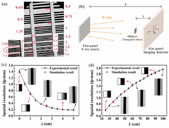
Figure 8. The imaging spatial resolution of a diagonal 4-inch X-ray source based on ZnO nanowires. (a) Contact image of a line-pair card. (b) Schematic diagram of the testing system. Dependence of spatial resolution on z (c) and L (d). Reproduced from [18], with the permission of IEEE, 2021.
2.4. Photodetector
Generally, there are two kinds of integrated photodetectors based on the ZnO nanowire cold cathode. One is to use a photoconductor material as the anode, the other is to fabricate a photoconductor material between the ZnO nanowires and the cathode electrode. Although both of them seem to work as a diode connecting with a photoconductor in series, their mechanisms are different. In the former case, as shown in Figure 9, Z. Zhang et al. [19] found that the electron bombardment on the ZnS photoconductor thin film can induce photoconductivity, which led to an internal photoconductive gain of above 104. While in the latter case as shown in Figure 10, the emission current density of ZnO nanorod on n-GaN fabricated by Y. Chen et al. [20]can only be improved from <3 to 8 mA/cm2 under UV illumination. Although their attempt is to utilize the positive-feedback enhanced emission current to pump the AlGaN semiconductor for a UV light source, their device also has photodetection capability due to the enhanced electron supply for injection from GaN to the ZnO nanorod. Therefore, their work is presented here for a comparison.
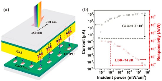
Figure 9. Demonstration of a photodetector based on a ZnO nanowire cold cathode. Schematic diagram (a) and performance (b) of the device. Reproduced from [19], with the permission of ACS Publications, 2018.
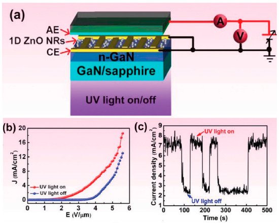
Figure 10. Schematic diagram (a), field-emission J-E characteristics (b) and time-resolved emission current density (c) of a ZnO nanorods/n-GaN photodector. Reproduced from [20], with the permission of RSC Pub, 2019.
In addition, a photodetector device based on a ZnO nanowires cold cathode has also been demonstrated for X-ray detection[21], in which a vacuum diode is connected with the photoconductor in series.
References
- Choi, W.B.; Chung, D.S.; Kang, J.H.; Kim, H.Y.; Jin, Y.W.; Han, I.T.; Lee, Y.H.; Jung, J.E.; Lee, N.S.; Park, G.S.; et al. Fully sealed, high-brightness carbon-nanotube field-emission display. Appl. Phys. Lett. 1999, 75, 3129–3131.
- Teo, K.B.K.; Chhowalla, M.; Amaratunga, G.A.J.; Milne, W.I.; Legagneux, P.; Pirio, G.; Gangloff, L.; Pribat, D.; Semet, V.; Binh, V.T.; et al. Fabrication and electrical characteristics of carbon nanotube-based microcathodes for use in a parallel electron-beam lithography system. J. Vac. Sci. Technol. B Microelectron. Nanometer Struct. 2003, 21, 693.
- Travish, G.; Rangel, F.J.; Evans, M.A.; Hollister, B.; Schmiedehausen, K. Addressable flat-panel x-ray sources for medical, security, and industrial applications. In Proceedings of the Advances in X-ray/EUV Optics and Components VII, San Diego, CA, USA, 13 August 2012.
- Zhang, Z.; Wang, K.; Zheng, K.; Deng, S.; Xu, N.; Chen, J. A flat panel photodetector formed by a ZnS photoconductor and ZnO nanowire field emitters achieving high responsivity from ultraviolet to visible light for indirect-conversion X-ray imaging. J. Light. Technol. 2018, 36, 5010–5015.
- Zheng, K.; Shen, H.; Li, J.; Sun, D.; Chen, G.; Hou, K.; Li, C.; Lei, W. The fabrication and properties of field emission display based on ZnO tetrapod-liked nanostructure. Vacuum 2008, 83, 261–264.
- Li, Y.; Zhang, Z.; Zhang, G.; Zhao, L.; Deng, S.; Xu, N.; Chen, J. Optimizing the field emission properties of ZnO nanowire arrays by precisely tuning the population density and application in large-area gated field emitter arrays. ACS Appl. Mater. Interfaces 2017, 9, 3911–3921.
- Liu, Y.; Zhao, L.; Zhang, Z.; Chen, D.; Zhang, G.; She, J.; Deng, S.; Xu, N.; Chen, J. Fabrication of ZnO nanowire field-emitter arrays with focusing capability. Trans. Electron Devices 2018, 65, 1982–1987.
- Cao, X.; Yin, J.; Wang, L.; Zhang, G.; Deng, S.; She, J.; Xu, N.; Chen, J.; Fabrication of coaxis-gated ZnO nanowire field-emitter arrays with in-plane focusing gate electrode structure. . Trans. Electron Devices 2019, 67, 677–683.
- Chen, Y.; Hu, L.; Song, H.; Jiang, H.; Li, D.; Miao, G.; Li, Z.; Sun, X.; Zhang, Z.; Guo, T. Optimized performances of tetrapod-like ZnO nanostructures for a triode structure field emission planar light source. Nanoscale 2014, 6, 13544–13549.
- Xu, J.; Zhang, Y.; Deng, S.; Chen, J.; Xu, N. 10 inch screen printed ZnO nanowire cold cathode for flat panel light source. In Proceedings of the International Vacuum Nanoelectronics Conference, Roanoke, VA, USA, 8–12 July 2013.
- Yin, J.; Chen, M.; Wang, L.; Cao, X.; She, J.; Deng, S.; Xu, N.; Chen, J. Cathodoluminescent properties of polycrystalline Ga2O3 thin film and its application UV flat panel light source. In Proceedings of the 33rd International Vacuum Nanoelectronics Conference, Lyon, France, 6–10 July 2020.
- Chen, D.; Song, X.; Zhang, Z.; Li, Z.; She, J.; Deng, S.; Chen, J. Transmission type flat-panel X-ray source using ZnO nanowire field emitters. Appl. Phys. Lett. 2015, 107, 243105.
- Chen, D.; Xu, Y.; Zhang, G.; Zhang, Z.; She, J.; Deng, S.; Chen, J. A double-sided radiating flat-panel X-ray source using ZnO nanowire field emitters. Vacuum 2017, 144, 266–271.
- Zhao, Y.; Chen, Y.; Zhang, G.; Zhan, R.; She, J.; Deng, S.; Chen, J. High current field emission from large-area indium doped ZnO nanowire field emitter arrays for flat-panel X-ray source application. Nanomaterials 2021, 11, 240.
- Cao, X.; Zhang, G.; Zhao, Y.; Xu, Y.; She, J.; Deng, S.; Chen, J. Fully vacuum-sealed addressable nanowire cold cathode flat-panel X-ray source. Appl. Phys. Lett. 2021, 119, 053501.
- Cao, X.; Zhang, G.; Zhao, Y.; Xu, Y.; She, J.; Deng, S.; Chen, J. Fully vacuum-sealed addressable nanowire cold cathode flat-panel X-ray source. Appl. Phys. Lett. 2021, 119, 053501
- Huang, Y.; Zhang, Y.; Gu, Y.; Bai, X.; Qi, J.; Liao, Q.; Liu, J. Field emission of a single in-doped ZnO nanowire. J. Phys. Chem. 2007, 111, 9039–9043.
- Huang, Y.; Zhang, Y.; Gu, Y.; Bai, X.; Qi, J.; Liao, Q.; Liu, J. Field emission of a single in-doped ZnO nanowire. J. Phys. Chem. 2007, 111, 9039–9043.
- Zhang, Z.; Wang, K.; Zheng, K.; Deng, S.; Xu, N.; Chen, J. Electron bombardment induced photoconductivity and high gain in a flat panel photodetector based on a ZnS photoconductor and ZnO nanowire field emitters. ACS Photonics 2018, 5, 4147–4155.
- Chen, Y.; Zhang, Z.; Jiang, H.; Li, Z.; Miao, G.; Song, H.; Guo, T. Realization of an efficient electron source by ultraviolet-light-assisted field emission from a one-dimensional ZnO nanorods/n-GaN heterostructure photoconductive detector. Nanoscale 2019, 11, 1351–1359.
- Zhang, Z.; Zheng, W.; Wang, K.; Chen, H.; Deng, S.; Chen, J. Sensitive and fast direct conversion x-ray detectors based on single-crystalline HgI2 photoconductor and ZnO nanowire vacuum diode. Adv. Mater. Technol. 2020, 5, 1901108.
More
Information
Subjects:
Nanoscience & Nanotechnology
Contributor
MDPI registered users' name will be linked to their SciProfiles pages. To register with us, please refer to https://encyclopedia.pub/register
:
View Times:
967
Revisions:
3 times
(View History)
Update Date:
06 Sep 2021
Table of Contents


Notice
You are not a member of the advisory board for this topic. If you want to update advisory board member profile, please contact office@encyclopedia.pub.
OK
Confirm
Only members of the Encyclopedia advisory board for this topic are allowed to note entries. Would you like to become an advisory board member of the Encyclopedia?
Yes
No
${ textCharacter }/${ maxCharacter }
Submit
Cancel
Back
Comments
${ item }
|
${ item.createdUser.fullName }
${ item.createdAt }
${ item.vote }
${ item.reply }
Delete
${ reply.createdUser.fullName }
${ reply.createdAt }
${ reply.vote }
Delete
There is no reply to this comment~
${ item.replyTextCharacter }/${ item.replyMaxCharacter }
Submit
Cancel
More
No more~
There is no comment~
${ textCharacter }/${ maxCharacter }
Submit
Cancel
${ selectedItem.replyTextCharacter }/${ selectedItem.replyMaxCharacter }
Submit
Cancel
Confirm
Are you sure to Delete?
Yes
No