The continuous down-scaling of complementary metal oxide semiconductor (CMOS) field effect transistors (FETs) had been suffering two fateful technical issues, one relative to the thinning of gate dielectric and the other to the aggressive shortening of channel in last 20 years. To solve the first issue, the high-κ dielectric and metal gate technology had been induced to replace the conventional gate stack of silicon dioxide layer and poly-silicon. To suppress the short channel effects, device architecture had changed from planar bulk Si device to fully depleted silicon on insulator (FDSOI) and FinFETs, and will transit to gate all-around FETs (GAA-FETs). Different from the planar devices, the FinFETs and GAA-FETs have a 3D channel. The conventional high-κ/metal gate process using sputtering faces conformality difficulty, and all atomic layer deposition (ALD) of gate stack become necessary. This review covers both scientific and technological parts related to the ALD of metal gates including the concept of effect work function, the material selection, the precursors for the deposition, the threshold voltage (Vt) tuning of the metal gate in contact with HfO2/SiO2/Si. The ALD of n-type metal gate will be detailed systematically, based mainly on the authors’ works in last five years, and the all ALD gate stacks will be proposed for the future generations based on the learning.
- COMS
- metal gate
- atomic layer deposition
- high-κ dielectric
- threshold voltage
- flatband voltage
- effective work function
- effective oxide thickness
1. Introduction
1.1. Scaling and Issues of SiO2/poly-Si Gate Stacks
where Tox is the layer thickness, ΦB the potential barrier height between the metal and the SiO2, Vox the voltage drop through the SiO2, m* the electron effective mass in the dielectric, and A an experimental constant. For a dielectric without defects, ΦB could be determined by the energy band alignment as shown in Figure 3. For electron transportation, the barrier is conduction band offset given as ΔEC. For hole transportation, it is valence band offset given as ΔEV. It is easy to see that Jg strongly depends on ΦB. In a real dielectric material, the barrier height is also relative to the defect density in SiO2. The defects could form energy levels in the SiO2 band gap and trap the charges. Such a trap-assisted mechanism of charge transportation can be described as Frenkel-Poole emission or hopping conduction [4].
The gate leakage depends strongly on Tox, as shown in Equation 1 and Figure 4. For the layers thinner than 1 nm, the extremely high tunneling leakage will cause intolerable power consumption and joule heat.
Figure 3. Band diagram of the poly-Si/SiO2/Si gate stack.
Figure 4. Gate leakage current density as a function of SiO2 physical thickness.
Reliability degradation is an equally important issue attributed to the dielectric down-scaling. Degraeve gave a fundamental mechanism of dielectric breakdown in a thin SiO2 film based on percolation model [5]. The breakdown occurs when the accumulation of different defects in the SiO2 network reaches the threshold and builds a conductive filament. Such a failure mechanism explains well the sensitivity of breakdown to the film thickness.
Another issue of the conventional poly-Si/SiO2 gate stack worsen by the dimension scaling is the boron penetration [6]. In a poly-Si gate, the carriers derive from the doped III or V valence elements. For a p-type poly-Si, boron is widely used as dopants. The boron ions in the heavily doped poly-Si could diffuse through the gate dielectric. For a thick dielectric layer, the diffusion could be very small. As the SiO2 is scaled to nanometer thick, the out-diffused B dopants accumulating in the SiO2 and Si substrate would change the threshold voltage, increase the defect density and further worsen the leakage and reliability issues.
1.2. High-κ Dielectric and Effective Oxide Thickness (EOT)
The solution to the issues above is to use an alternative dielectric which has a dielectric constant, or κ-value, higher than SiO2 and allows physical thickness larger than SiO2 without tradeoff in gate capacitance. For a simplified model, the capacitance between the gate and the channel can be expressed as
(2)
where κ is the dielectric constant, ε0 the permittivity of free space (= 8.85 × 10⁻³ fF/fm), S the area, and t the thickness of the dielectric. For SiO2, κ is around 3.9. If a high κ material is used as gate dielectric, a thicker layer could give the same capacitance density, or for a high-κ layer of a given thickness (thigh-k), the capacitance density generated equals to that of a SiO2 layer of tox, This tox is called equivalent oxide thickness (EOT)
(3)
For example, to retain an EOT of 1nm for a dielectric with a κ-value ~20, the physical thickness of the high-κ could be ~5 nm. The increase of the physical thickness could help to suppress the gate leakage.
First industrial application of alternative dielectric concept was to alloy nitrogen into SiO2 to form so-called silicon oxynitrides, whose κ value is slightly higher than SiO2 and thus allows larger physical thickness than SiO2. The κ-value of pure Si3N4 is around 7, compared to that of SiO2 about 4. That of SiOxNy is between 4 and 7, depending on the nitrogen concentration in the films. Encouraging results in leakage current reduction, boron diffusion control, and reliability enhancement were demonstrated by using SiOxNy to replace SiO2 of the same EOT [7-9]. The leakage suppression of SiOxNy depends on the layer composition. A work done by Yang and Lucovsky [10], for instance, demonstrated a 100× leakage current reduction using a layer with a SiO2: SixNy ratio of 1:1 and EOT of 1.7 nm. The advantages of SiOxNy lie in that it guaranties the safety in contamination control, because nitrogen is a widely used element in IC production and the compatibility to conventional poly-Si. It has been found that the addition of N to SiO2 can form Si–O–N network bonding and greatly block the boron diffusion through the dielectric [11, 12]. The reason for using SiOxNy instead of pure Si3N4 is that the former shows much better channel mobility [13]. The mobility degradation attributes to the pentavalent N at interface, which induces defects and aggravate the interface scattering. For SiOxNy layers, especially those with graded N concentration, the interface defects density could be much less than the pure SiNx. The SiOxNy dielectric was used for a few technology nodes. By increasing the N concentration node by node, the scaling strategy was successfully extended from 130 nm node to 65 nm node. The SiOxNy solution can only temporarily alleviate the gate leakage crisis. When EOT is below 1.3 nm, it does not work anymore and a new alternative has to be found from “real” high-κ candidates [14].
A high-κ dielectric must have a high κ-value, large enough band offsets with Si, and be thermally stable when contacted with the gate electrode and Si, and its impact to channel mobility must be acceptably small [15-17]. Figure 5 lists the dielectric properties of most important gate dielectric candidates. Among all of them, SiO2 has the lowest dielectric constant and the largest conduction and valence band offsets. For the others, the band offsets decrease when the k-value increases. The decrease in conduction band offset will trade off the positive effect in leakage suppression due to the thickness increase. Therefore, an ideal high-κ should have a balance between the κ value and band gap. The films with ultra-high κ value and very small band offsets, such as TiO2, are thus out of consideration. Furthermore, ultra-high κ value means a very thick dielectric and a large thickness/length ratio. An undesirable effect, the fringing effect of the gate stack, will become extremely high [18].
Besides the κ-value and band alignment, attention must be paid to the interfacial quality between the high-κ dielectric and Si. The high leakage has been found due to the degradation of the interfacial oxide between the high-κ and the Si [17]. The defects near the interface could reduce the barrier height ΦB, and induce carrier scattering, causing the degradation of the channel mobility.
Figure 5. Comparison of the dielectrics in conduction and valence band offsets and permittivity.
Thermal stability of the high-κ stack is another filter. In fact, plenty of metal oxides have higher κ-values than Si dioxide, from Si3N4 with a k~ 7 to PbLaTiOx with a k-value as high as 1400 [19, 20], most of them in a stack in contact with Si shows poor stability at high temperatures, and thus eliminated from the list. Other properties, such as breakdown properties, adhesion with the top metal layer and bottom Si substrate, the temperatures of deposition and annealing, and readiness to be patterned with available lithography, should also be taken into account. After the elimination, very limited candidates are left in the list. The finally crowned high-κ dielectric by industry is HfO2 [21-24].
HfO2 has a κ-value about 25, a bandgap around 5.7 eV, yielding large enough band offsets with Si. Its large formation heat (-271 kcal/mol, compared to that of SiO2 ~−218 kcal/mol) guaranties good thermal stability in contact with silicon. The gate leakage current of the MOSFETs using a HfO2 dielectric show several orders of magnitude reduction compared to that of SiO2 with the same gate capacity [25, 26].
1.3. Metal Gate and Effective Work Function (EWF)
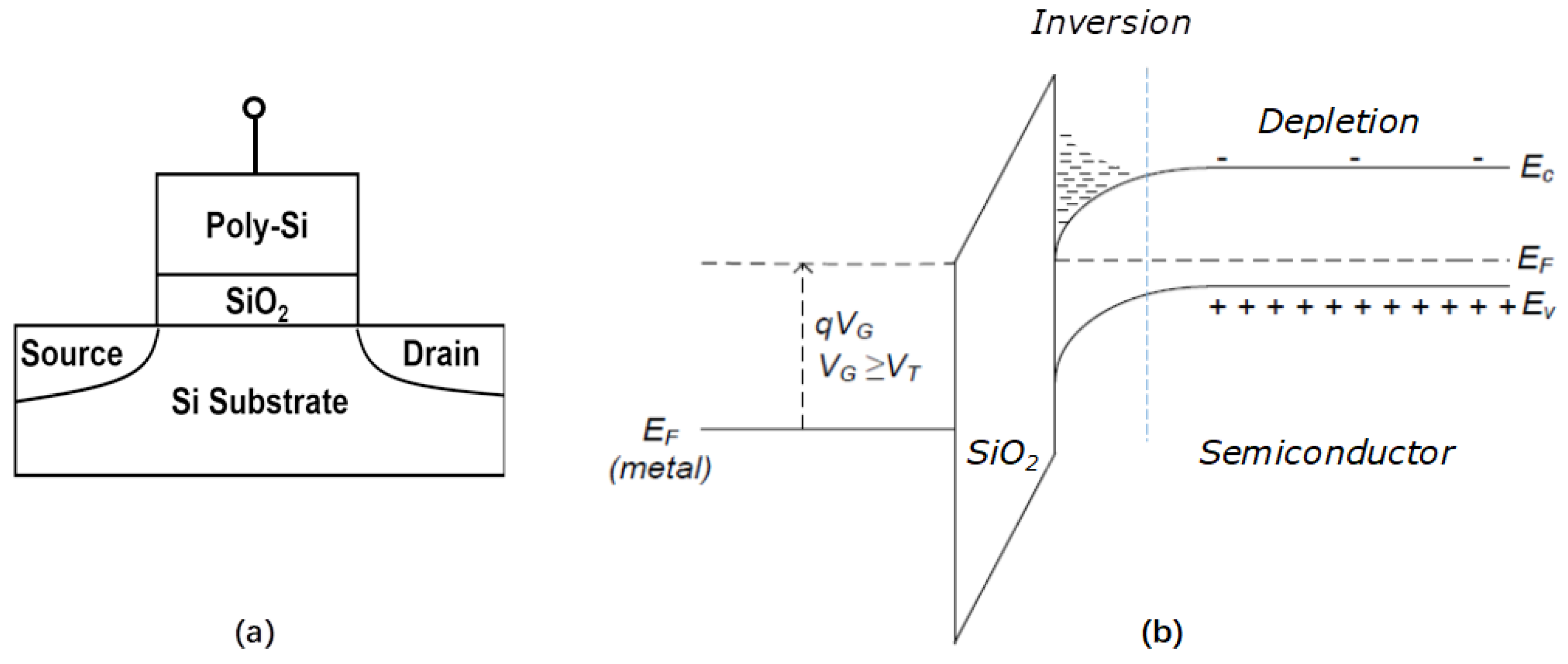
Another important issue relative to the dielectric thickness scaling is the depletion layer formed in the poly-Si gate near the interface of the gate and the dielectric, as shown schematically in Figure 6. The thinner is the dielectric, the stronger the field is generated by the channel inversion, and the more charges are involved in the depletion layer. The depletion layer forms an additional capacitor over the dielectric and impairs the impact of the gate voltage to channel. The thickness of the depletion layer is related to the carrier density of the poly-Si gate. The increase of doping level in the poly-Si can help to reduce the depletion thickness. The effort in employing more aggressive implantation for heavier doping poly-Si could induce grievous impurity penetration through the gate oxide [27]. Limited by this, the doping level of the n+ poly-Si is normally below 1020 cm−3 and that of p+ poly-Si is less than the mid of 1019 cm−3. This means that the depletion issue could not be released via increasing doping level. Beyond the 65 nm node, the poly-Si gate had to be phased out and replaced by metal gate electrodes.
Figure 6. Depletion layer formed in poly-Si. (a) schematic of a MOSFET; (b) band structure of poly-Si/oxide/semiconductor.
Figure 7. Work function of metals.
The work function is the first requirement for the metal gate electrodes. At beginning, the selection of the metal gate candidates was based on their work function in vacuum. Figure 7 lists more than 20 metals and their vacuum work functions [28]. When a metal is in a MOS structure, its work function shifts from its vacuum value. This value is normally termed as “effective work function or EWF”. EWF could be extracted from the C-V curves obtained with the MOS capacitors (MOSCAP) [29]. Figure 8 displays the simplified energy band diagram of an ideal MOS structure using n-type substrate under the condition of flat band, where ΦM stand for the work function of the metal, χ for the electron affinity, Eg for the band gap, ΦB for the potential barrier between the dielectric and metal, and ΨB for the difference of potential between the Fermi level EF and the intrinsic Fermi level at the midgap. Here, “ideal” means the fixed charge density in the dielectric is zero. As applied voltage is zero, the MOS structure has a flat band as shown in Figure 8, or the difference between the work functions the metal and the semiconductor, ΦMS, is zero. For n-type substrate
(4)
C-V measurement will give the curve as shown in the right plots of Figure 8. For p-type substrate, the case is similar. The ΦMS is
(5)
For real dielectric with a fixed charge density of (± Qf), the C-V curve will shift as shown in the plots. To have a flat band, a voltage of Vfb needs to be applied to shift the curve back.
(6)
Assuming the Qf is independent of EOT, the measured Vfb as a function of EOT will intercept the y-axis at ΦMS. Using this intercept value and the band structure of the dielectric, the effective work function of the metal ΦM could be extracted.
Figure 8. Flatband conditions of MOS structure for n-type substrate.
The metal gate for CMOSFETs can be a single metal with one EWF near midgap or two different metals (dual metal gate), one with EWF near the edge of the conduction band, and the other near that of the valance band, separately. Equation 7 gives the Vt as a function of Vfb.
(7)
Where the Qs is substrate charge density corresponding to the substrate surface potential of inversion mode (2ψB), N the substrate doping concentration, Ci the gate oxide capacitance, εS the substrate permittivity. The single metal gate is the most straightforward solution, favorable to the CMOS processing. However, this approach is not favorable in device performance. The midgap work function induces high Vt and poor operation channel current. It has to be pointed out that the above conclusion on the single metal solution is true only for planar CMOS using bulk Si substrate. For the devices such as undoped FinFETs and FD-SOI FETs, it is more complex [30, 31].
For the dual-metal gate CMOSFETs, the ΦM of the gate electrode for nMOS is expected to be ~ 4 eV and that for pMOS ~ 5 eV [32]. Since the EWF vacuum work function could not be used as the screening criteria, the study of metal gate properties needs to be done in a real gate stack with selected high-κ material and carefully designed stack structure. To reach threshold voltage (Vt) target, extreme care needs to be taken, because Vt is so sensitive to interfacial states that any slight difference in chemical composition, defects and polarization will induce Vt shift.
The thermal stability of the metal gate had been regarded as a fateful technical block for the industrial application of high-κ/metal gate stack. The harshest thermal process in CMOS production is the annealing for dopants activation in the area of source and drain. In most cases, a rapid thermal annealing (RTP) between 900–1100 °C is employed. The work function of most metals will shift back to midgap after this annealing. This is why the metal gates studied in the early explorations all have good refractory. They include elemental metals, their oxides, silicides, nitrides, carbides or alloys of more than two of them. Most of them, when being in contact with the selected high-κ, could not keep stable at high temperature. After the activation annealing, the EWF shifts.
To bypass the thermal instability problem, a new processing flow, the gate-last approach, has been developed [25]. In such a process, the high-κ is first deposited, followed by the conventional poly-Si gate process to form a poly-Si “dummy” gate. This conventional flow continues until the activation anneal is finished. Then, the poly-Si gate is removed before the deposition of the metal gate layer, capping layer and filling metal. In such a “replacement gate” regime, the source/drain activation anneal is carried out before the metal gate deposition and thus successfully avoids the Vt shift related to the activation anneal.
In the 45 nm node, the first generation of the high-κ/metal gate technology for mass production, dual metal/single high-κ stack was used. The metal gate for nMOS was TiAl, and that for pMOS was TiN, integrated with HfO2 dielectric by a gate last process [25, 33] The TiAl and TiN were deposited in the trench on the bottom after the replacement gate removal. To fill the gap, a conductive metal such as Al or W was deposited.
TiN in the stack with HfO2 has a EWF range between 4.4 and 4.9 eV, depending on processing technique used and the metal layer thickness [34, 35] and meets the requirement for pMOS. TiN is a widely used material in conventional IC process, so induces no contamination risk. Its deposition, etching and cleaning techniques are well developed using industrial standard equipment. During 2003–2006, a lot of works presented at device conferences on the integration technology used high-κ/TiN metal gate stack, where TiN were deposited by PVD or CVD [36-42].
Aluminum metal has a work function around 4.28 eV and good conductivity, and thus is a candidate of n-type metal gate. Its melting point, however, is quite low (~660 °C), implying a poor thermal stability. Alloying Al into more refractory metal to form alloy was one of the research directions [43]. Doping Al into PVD TiN, for example, can shift the EWF from the value near the bottom of the Si conduction band to that near the top of the valence band [44] and get different flatband voltages in TiN(Al)/HfO2/Si stack. In 2010, Kesapragada et al. reported a work function screening result for gate last process and proposed the combination of PVD TiAl for n-type metal with PVD TiN for p-type metal. The PVD TiAl and PVD TiN in gate stacks with HfO2 show EWF around 4.1 eV and 4.85 eV. The C-V measurements show that the PMOS using HfO2/PVD-TiN and the NMOS using HfO2/PVD-TiAl have 1 volt separation in Vfb [45]. Intel seemed to use this combination for their planar CMOS integration, and got working high-performance devices with large gate leakage current reduction [25].
1.4. Metal Gate for FinFETs and GAA-FETs
Gate leakage is not the only issue relative to the dimension scaling. Compared to a long channel MOSFET, the shrinking of channel length will reduce the gate control ability [46-48]. First, the current at Vg < Vt (subthreshold leakage) will increase along with the gate length shrinking, inducing so-called subthreshold swing, SS. Second, for short channel devices, Vt is also a function of the voltage between drain and source, VDS, certain charges are depleted by the VDS. As a result, the gate voltage required to form the channel is lowered by VDS. This is called drain induced barrier lowering (DIBL). Third, for short channel devices, the potential of source and drain will also impact the channel, making the channel formation at lower Vt. The shorter is the channel, the smaller is the Vt. This is referred to as Vt roll-off.
All these short channel effects could be suppressed by changing the device structure from planar MOSFETs to FinFETs [49] and gate-all-around (GAA) FETs [50]. The FinFETs have become the mainstream logic devices for a few nodes [51]. The GAA nano-Si wire FETs and Si nano-sheets FETs have been reported by the research teams using industrial processing facility [52-57].
The relation between Vt and the work function of the gate electrode for FinFETs with undoped channel is different to that for the planar MOSFETs. For planar devices, there are plenty of charges to form inversion. For undoped FinFETs, much less charges are available. As a result, an additional surface potential needed to reach the Vt. W. Xiong summarized the relation of the Vt and work function of the gate electrode for low-power and high performance planar MOSFET and FinFETs in a schematically way as in Figure 9 [58]. The points in the top and bottom green rectangles give the Vt requirement of different low power devices and high performance devices, respectively. The points in the rectangle with yellow color give the work function requirement of bulk planer NMOSFETs and PMOSFETs. The points in the triangle give the work function requirement of FinFETs. For low power FinFETs, a metal with a work function of 4.6 eV in the midgap of Si can meet the requirement for both n-type and p-type devices. High performance devices desire low threshold, and thus two metals with work functions near the edges of the conduction band and valence band of Si are needed. Different from the metal gates for the planar CMOSFETs, which needs two metals with work functions 0.4 eV from the midgap, those for the FinFETs can use metals with work functions 0.2 eV from the midgap. The work function values of FinFET are about 4.4 eV and 4.85 eV for N metal and P metal respectively, while the values are about 4.2 eV and 5.0 eV for planar CMOSFETs.
Figure 9. The relation between the threshold voltage and the work function of the metal gate for different devices.
Senzaki et al. [59] gave the other specifications include Vt stability (~ ±10 mV of unstressed film), Mobility ≥ 95% of that achieved with SiO2, density of interface traps (Dit) ≤ 5 × 1010 cm−2⋅eV, high frequency (100 kHz) CV hysteresis ≤ 10 mV, Reliability comparable to Poly-Si/SiO2, and thickness uniformity (3 sigma) ≤ 4%.
For FinFETs and GAA FETs, the conformality of the metal gate is a new challenge. In a planar device, the metal film could be deposited top-down by sputtering. For FinFETs, it is very difficult to form conformal film on sidewall of the Fins using these anisotropic deposition techniques. CVD technique has much better isotropy than PVD and is most likely able to meet the requirement of FinFETs. For GAA FETs, however, both PVD and CVD will be phased out from the deposition of gate layers, replaced by ALD. The advantages of using ALD to deposit metal gate can be summarized as: excellent thin film thickness uniformity, excellent composition control (doping by inserting dopant layers), little plasma damage to gate oxide (especially for thermal ALD) compared to PVD, lower deposition temperature with low impurity compared to CVD, and conformality at nanoscale structures, especially for 3D devices [59].
2. ALD of the Metal Gates
Atomic layer deposition is a derivative of chemical vapor deposition (CVD), using the same reactants but different reactant introduction mode, to have a thickness control of mono-atomic layer level [60]. In CVD, the reactants, say AC and BD, are introduced together simultaneously and continuously into reaction chamber and the chemical reactions takes place in gas phase, or on the top surface of the substrate after absorption, to form a deposit AB. For ALD, the reactants are introduced separately and sequentially, in different pulse steps separated by purge step. A typical ALD cycle is composed of four sequential process steps: pulse of AC, purge, pulse of BD, purge. If the pulse steps are long enough, AC or BD could react with the pre-deposited B or A at all possible sites on the exposed surface of the substrate and finish a surface saturation reaction. After the saturation, no more sites are available, and the reaction will be self-limited. The introduction of the reactants will stop, and the residual gas purged by the inert gas. An ideal ALD cycle deposits only one monolayer of the atom. The merit of ALD is that its outstanding thickness uniformity and isotropic characteristic, since the surface reactions during the two pulse steps are self-limited.
Similar to CVD, most of ALD is thermal ALD, or it takes place at high temperature. This limits it from the applications which cannot stand the deposition temperature. To lower the deposition temperature, plasma is used to enhance the ALD reaction. The choice between the thermal ALD and the plasma-enhanced ALD (PEALD) should depend on the requirement of the application. For the deposition of high-κ and metal gate, PECVD is not a favorable technique, because the plasma might induce surface damage of the delicate gate area [61, 62]. If a thermal ALD with acceptable deposition temperature is available, PEALD will be given up. In the following paragraphs, the ALD of p-metal gate and n-metal gate is discussed.
2.1. ALD of P-Type Metal Gate
The top-ranking candidates for p-type metal gate included refractory element metals such as Ru, Pt and W. It is interesting to note that all these three metals are also among the very limited number of metals which could be deposited by ALD.
Ru and RuOx: the ALD of Ru was widely studied [63-66]. Because of its high work function (~4.7 eV) and conductive oxides, it is expected to be suitable to applications as p-type metal gate electrodes for SrTiOx MIM capacitor for DRAM [67-69] and seed layer of Cu plating for back end of line process of CMOS [70-72]. A nice summary on the precursors available for the ALD of Ru and the deposition reactions can be found in the reference [72]. The precursors used for Ru are mainly cyclopentadienyl compounds such as RuCp2 (Cp = cyclopentadienyl) and Ru(EtCp)2 (Et = ethyl), and β-diketonate compounds like Ru(od)2 (od = 2,4-octanedionato) and Ru(thd)3 (thd = 2,2,6,6-tetramethyl-3,5-heptanedionato) [67, 68]. The mechanisms of the processes are based either on oxidation of the ruthenium precursor by oxygen or on reduction by NH3 plasma.
Although so much effort has been made, the quality of the ALD Ru layer does not seem qualified for work function metal application. Up to now, no matter which precursor used, the ALD of the Ru all have remarkable incubation cycles, inducing surface roughness [72]. They are probably matured for the application of the MIM capacitors and interconnections, but not for the work function layer of the metal gate.
Platinium: ALD of Pt has also been widely studied in the last 20 years because of its excellent chemical and thermal stability and conductivity for potential applications such as the electrodes for ultra-high κ in the cell of DRAM and those for ferroelectric dielectric in FERAM [67, 73-76]. Its high work function (5.6 eV) and low resistivity (10.5 μΩ·cm) also attracted the attention for the application as p-type metal gates [77].
The ALD of platinum has been studied using two different kinds of compounds, MeCpPtMe3 (Me = methyl) [67], and Pt(acac)2 (acac = acetylacetonato), as precursors, and O2, pure or in air, and H2, as reactant [67, 78]. For the ALD using MeCpPtMe3, the precursor would dissociate when chemically absorbed on and reacted with the O in previously deposited layer. For that using Pt(acac)2, both oxygen and hydrogen could react with the precursor, the ALD with hydrogen, however, could only grow a very poor film at low deposition rate. Mackus studied the mechanism of the ALD using MeCpPtMe3 [79], and indicated that the ALD behavior is relative not only to the reaction between the precursor and O2, but also to the catalytic nature of the Pt film, based on their observation of the gas products generated. The mechanism was described as a series of reactions in sequence; the combustion and dehydrogenation reactions in MeCpPtMe3 pulse on the O covered surface, formation of a carbonaceous passivation of the surface, and the combustion of the carbonaceous layer in O pulse. It was believed that it was the carbonaceous passivation which attributes to the self-limitation and the temperature dependence of the deposition rate. Henkel’s work studied the electrical performance of the Pt metal gate in the stacks with Al2O3, ZrO2 and SiO2 [76, 77]. They found that the EWF of the ALD Pt strongly depended on the dielectric, 4.76 eV for ZrO2, 5.22 eV for Al2O3 and 5.52 eV for SiO2. The MOS capacitors using the ALD Pt on ZrO2 and Al2O3 also showed good defect density control and leakage reduction.
A concern on the application of Ru and Pt as the work function metal might lie in the difficulty of wet clean. These noble metals are chemically inert and any contamination of them on the backside of the Si wafers needs a very harsh wet process to be removed. When being used as the metal gate, CMP process will inevitably induce backside contamination. This might explain why the two metals, after extensive investigations, have never been employed in front end of line of the CMOS production.
Tungsten: The ALD of W is the most successful case among elemental metal ALD processes. Thanks to sound study on the CVD of W, inorganic precursor WF6, and reducing reactants, silane or borane compound and their reaction mechanisms have been well known. The first study on the ALD of W was reported by Klaus et al. in 2000 [80]. They studied the ALD on SiO2 using WF6 and Si2H6 and demonstrated a linear growth of W at temperatures below 350 °C, without any incubation. The mechanism of the deposition was explained as the self-limited reaction in that Si2H6 strips fluorine from WFx species and the resulting SiHyF species are subsequently removed by the next WF6 exposure. Elam et al. [81] further studied the nucleation of the above deposition. Slightly different from the previous work, an incubation of five cycles is found, believed to attribute to the nucleation on the OH-group finalized SiO2 surface. The ALD-W films deposited by using diborane, B2H6, as a reducing agent of WF6 was reported in 2002 by Yang et al. [82] and further studied by Kim et al. [83, 84]. The ALD-W process using silane, SiH4, was also extensively investigated, based on the similar reaction mechanism consideration [85, 86]. All the above works were mainly targeting the application as the seed layer of CVD for W contact plug. Wang et al. studied the ALD W on TiN using SiH4 and B2H6 as the metal for filling the high aspect ratio gap of the replacement gate [87, 88]. A good gap filling capability and electrical performance was demonstrated with MOSCAP and pMOSFETs. The comparison of the properties between the ALD W using SiH4 and B2H6 for the replacement gate filling in the pMOSFETs revealed that the former, which is crystalline and has a much larger tensile stress (~2.4 GPa), could give superior electrical properties compared to the B2H6-generated layer.
ALD W is less favorable for being used as the work function layer of the metal gate, due to its near midgap work function (~4.6 eV) [89], the usage as filling metal for all-ALD gate stack is without doubt promising.
TiN: TiN was first introduced in the 1970s, deposited by reactive sputtering using Ti target and reactive gases such as NH3 and N2. Its excellent hardness, density, melting point and gold-like appearance attracted so much attention for the applications as abrasion-resistive or decorative coating. Quite unusual, such a nitride film has a high electrical conductivity. In semiconductor industry, it has been used as an inorganic antireflective coating for lithography [90], hardmask for low-κ patterning [91, 92], and diffusion barrier for tungsten contact and Cu interconnection [93, 94].
As mentioned before, TiN was successfully used as a p-metal gate in the first generation high-κ/metal gate technology. In fact, TiN is an ideal candidate for the metal gate because of its excellent thermal stability in contact with HfO2, low resistivity and compatibility to conventional CMOS process [95-97]. Since conformality is difficult to achieve by PVD, extensive exploration of CVD techniques for TiN deposition has been carried out over the last 20 years, with variations such as PECVD [98, 99], low-pressure CVD (LPCVD) [100, 101], atmosphere pressure CVD (APCVD) [102, 103], metalorganic CVD (MOCVD) [104, 105] and low pressure metalorganic CVD [106, 107].
ALD of TiN was first explored by Hiltunen et al. in 1988 [108] and by Ritala et al. in 1995 [109]. Using TiCl4 as precursor and NH3 as reactant, polycrystalline TiN was deposited on glass at 500 °C. It was found that the deposition rate is below 0.02 nm/cycle, corresponding to 0.1 monolayers of the (111) direction per cycle. These TiN layers have clorine content less than the detection limit of the Rutherford Back scattering (RBS) and hydrogen impurity less than 0.4 at%. The oxygen content of the films is about 3 ± 2% in 1400 Å thick film and it is relatively higher in thinner film. The oxygen incorporation may be due to the oxidation of the film after the deposition. Thinner film is easier to oxidize. The oxidation will happen in all the other TiN films, including the films discussed in the following sections.
ALD with TiI4 and NH3 was also tried based on the consideration on the difference in dissociation energy between Ti-I (D0 = 296 kJ/mol) and Ti-Cl (D0 = 429 kJ/mol) [110]. Lower deposition temperature is expected for the ALD with TiI4-NH3 than TiCl4-NH3. The experiments showed that TiN layer could be deposited at 350 °C. At 500 °C, the deposition rates of the TiI4-NH3 is slightly higher than the TiCl4-NH3. The film deposited at 350 °C has 2 at% iodine content, and for those deposited at temperatures exceeding 400 °C, iodine content is below 0.5 at%. The oxygen content, however, was similar (10 at% at 400 °C) to the films by TiCl4 -NH3 process. At 350 °C, 40 at% oxygen was incorporated in the film. As a result, the resistivity of the films decreased as a function of the deposition temperature.
The ALD of TiN on Si was studied by Jeon et al. [111]. Better quality of TiN was demonstrated at 350 °C with chlorine content of about 3 at%. The most important difference between these processes and that of Ritala et al.[110] is in NH3 flow rate. Jeon et al.[111] deposited TiN films using the flow rate of 75 sccm, which is nearly 10 times higher than used by Ritala et al.[109] This might attribute to the difference in film quality at 350 °C.
The above works using Ti halides show a very low deposition rate at the temperature range compatible to CMOS process. To solve the problem, organic metal precursors were tested, based on the experience in MOCVD [112-114]. With CVD technique, TiN films could be grown at low temperatures with different titanium alkylamides [115]. Although the compounds include the Ti-N bond, external nitrogen source such as NH3 is still needed since the simple decomposition of the alkylamides is not enough to achieve qualified films [116]. The ALD of TiN have been carried out with Ti[N(C2H5CH3)2]4 (tetrakis(ethylmethylamido)titanium, TEMAT) and NH3 as well [113, 114]. It was found that the self-limited ALD reactions take place in the temperature range of about 150 - 220 °C. At higher temperatures, TEMAT decomposed and CVD type reactions became dominant. The growth rate of these films was 10 times higher than in the halide based processes, varying between 0.5 - 0.6 nm/cycle. This is even higher than the ideal monolayer per cycle (ML/cycle) and was explained by a model of re-chemisorption of the precursor and NH3. The films showed low impurity level, with only 4 at% carbon and 6 at% hydrogen incorporation and excellent step coverage above 90%. J. Musschoot et al. studied the ALD of TiN from tetrakis(dimethylamino)titanium (TDMAT) [112]. Both thermal and plasma enhanced processes were studied, with N2 and NH3 as reactive gases. A growth rate of 0.06 nm/cycle was achieved with an optimized thermal ALD process, comparable to the ALD using TEMAT. The thermal ALD films had very high impurity level with about 37% oxygen and 9% carbon.
The above early ALD studies to deposit TiN were targeted at the application of tungsten and Cu diffusion barriers. The first study on the ALD of the TiN for the metal gate application was reported in 2002 by Lujan [117]. In their work, the thermal ALD of TiN was carried out with TiCl4 and NH3 at 350 °C and annealed in forming gas at 420 °C for 30 min to passivate interface states. The flatband voltage (Vfb) was extracted from the C-V curve and used to calculate the EWF. It was found that the Vfb of the ALD TiN is comparable to that of the p-type poly-Si. The EWF extracted is about 5.3 eV. In the same work, they compared the C-V curve of the ALD TiN with PVD TiN and found that the PVD TiN had a mid-gap work function. The p-type EWF of the ALD TiN was explained as more N incorporated in the film. The processing details and growth mechanism were presented by Besling et al. and Satta et al. [118, 119]. Park et al. published a work on the ALD of TiN in the same year using the same precursor and reactant [120]. They studied the W/TiN/SiO2(3 nm)/p-Si MOS capacitors and demonstrated that the ALD–TiN has very low interfacial defect density on SiO2. The comparison among the ALD, and CVD revealed that the ALD layer had lower level of Cl content. F. Fillot et al. studied the ALD of TiN on ALD HfO2, using TDMAT and NH3 [121]. The ALD of TiN was carried out at 180 °C, and gave out a layer with 27 at% Ti, 30 at% N, 37 at% oxygen and 6 at% carbon. Different from the EWF reported by Lujin [117], this MOALD TiN showed a EWF of n-types metal, ~4.2 eV. This EWF was attributed to the interfacial layer generated by incubation of the deposition. They detected an interfacial layer of ~2 nm in the TiN, with remarkable Ti-rich composition. To confirm this, a follow-up study was done using the same ALD to investigate the impact of the TiN thickness to the EWF [122]. It was found that the flatband voltage of the TiN layer below 2 nm showed strong thickness dependence. After 2 nm, the flatband voltage approach constant.
Thermal stability was the most important concern for the application of the TiN metal gate. In 2003, Westlinder et al. studied the thermal stability of the ALD TiN with capacitors of Poly-Si/TiN/SiO2 [123]. The capacitors were annealed in the temperature range of 400 °C to 1000 °C in steps of 100 °C in an RTP furnace in N2 ambient for 30 s. In addition, some samples were annealed in nitrogen diluted with 10 at% oxygen at 400 °C for 30 s. It was found that the work function of the TiN could remain p-type up to 700 °C and would shift to midgap after annealing at temperatures higher than 800 °C. This was concluded, based on the requirement of gate first process, as a disappointing result for the application, as the p-type metal gate cannot survive from the source/drain activation annealing at 1050 °C. In 2010, L. Wu [124] reported a study on the thermal stability of the TiN/HfO2/Si stack, where HfO2 was deposited by ALD using HfCl4 and water, and TiN by ALD using TiCl4 and NH3. The work focused on the chemical stability of the stack after annealing at 1000 °C and revealed unsatisfactory thermal stability again.
It needs to be noted that the above thermal stability studies misfocused at a wrong temperature range, based on the assumption that a metal gate step must be processed before the activation anneal. Actually, if a gate last process employed, the thermal stability of the p-type Vt up to 700 °C is quite positive. In 2015, Brennan compared the electric properties of the TiN/SiO2/Si MOS capacitor (MOSCAP) and CMOSFETs of FDSOI with the TiN deposited by PVD and PEALD to trace the plasma damage to the dielectric [125]. The PEALD was carried out using TDMAT and H2/N2 under well controlled plasma condition for much lower ion dose and energy compared to PVD. The MOSCAP with PVD TiN clearly showed larger trap density and higher interfacial defect density than the PEALD. The n- and p-MOSFETs with PVD and PEALD TiN had similar electrostatic performance, with very good short channel performance, say small subthreshold swing, DIBL and Vt roll-off. The gate dielectric quality of them, however, are remarkably different. The gate leakage of those with PVD TiN was much higher than PEALD, consistent with the high density of defects in the bulk SiO2 leading to trap-assisted tunneling and significantly higher gate dielectric failure probability. Taken together, the electrical results suggested that during PVD of TiN, the gate dielectric was damaged by energetic ions and ultraviolet (UV) photons which break Si-O bands and leave defects states, inducing increased gate leakage and reliability issues.
In summary, most of the research works on TiN ALD were carried out using TiCl4 and NH3 or TDMAT and NH3, with and without plasma enhancement. In most cases, the chloride based ALD has a p-type work function [117, 123], while the TDMAT-based process gave a n-type work function [121, 125], compared to the midgap one of the TiN by PVD [126]. It was attributed to the different chemical composition of the interfacial layer. The TiCl4–based process could generate a Ti-rich interfacial layer, and thus had a Ti-like work function. The PVD TiN had a Ti:N ratio near 1:1, and as a result, had a work function at midgap. The TDMAT process generated TiN with high oxygen and carbon content, inducing n-type metal behavior. Real mechanism of the difference might be more complex. Many works revealed that the EWF of the TiN in the gate stacks shifted with the thickness [97, 127], post deposition anneal [97, 128], microstructure of the TiN [129, 130] and different doped ions such as Al [44], As [131], P/BF2 [132]. Careful engineering of the ALD TiN is always needed for the application in real gate stacks.
2.2. ALD of N-Type Metal Gate
Compared to the p-type metal gate, the selection of n-type metal gate is more difficult. The first demonstration of a dual-metal gate CMOS using Ti as n-metal gate and Mo as p-metal gate, respectively, together with SiOxNy as dielectric, was reported in 2002. The device showed negligible gate depletion, remarkably reduced gate leakage and acceptable channel mobility [133]. The TiN/Ti double layer was deposited by sputtering, targeting at a theoretical work function of metal Ti on SiOxNy of 4.36 eV. The EWF extracted, however, from the C-V measurements is 4.56 eV, near the midgap value for TiN. The complete silicidation of the poly-silicon gate electrode, called FUSI, was also proposed for dual gate application [134]. In the FOSI process, poly-Si is first deposited on SiON and doped by B and As for pMOS and nMOS, respectively. Afterwards, a thick enough Ni layer was deposited on the poly-Si, followed by annealing for silicidation. Two different work functions, ~4.5 and ~4.9 eV for NMOS and PMOS, respectively, were obtained. This approach attracted much attention at beginning [135], due to its integration simplicity, but was finally abandoned due to the difficulty to achieve low enough Vt devices. Another dual metal gate integration work [136] used PVD Ru as p-type metal and PVD TaC as n-type metal, and HfO2 as dielectric, demonstrated good device behavior. As mentioned before, the first industrial high-κ/metal gate technology for 45 nm node, reposted in 2007, used TiAl alloy as n-type MOSFETs [25]. The capacitor using AlTi n-type metal and HfO2 showed an ideal C-V curve and n-type EWF [45]. In all the above works, the n-type metal gate were deposited by PVD.
The first work on ALD of n-type metal was reported in 2007 by Triyoso using TaCy as the metal gate and HfO2 as the dielectric [137]. The TaCy films deposited by PEALD using organic precursor and a carbon containing gas was near-stoichiometric, nitrogen free, and had low oxygen impurities and amorphous carbon content. Excellent electrical properties using this TaCy/HfO2 stack were demonstrated, including work function between 4.77 and 4.54 eV and low fixed charge density (~2–4 × 10⁻¹¹ cm−2). Jeon et al. studied the ALD of TiN-TiC mixture using a fine designed precursor and process [138]. The TDMAT was used as precursor for Ti, H2 and NH3 as reactants. The sequence of one ALD cycle was designed as 1s TDMAT pulse/3s Ar purge/3s H2 plasma/1s (H2–NH3) preflow/3s (H2–NH3) plasma/3s Ar purge. The temperature range of pure ALD mode deposition was found between 150 °C and 200 °C, generating a layer of TiN. The deposition between 200 and 350 oC formed a mixture of TiC and TiN. The higher the temperature, the higher the TiC content will be. The EWF extracted from C-V measurement of MOSCAPs showed a decreasing trend from 5.02 eV for TiN to 4.8 eV for 18.5% TiC and 4.6 eV for 39% TiC. Such a tunable EWF was promising for dual gate CMOSFETs and multi-Vt applications. The CVD mode for TiC formation seemed a potential risk of causing processing variation.
Based on the encouraging results of PVD TiAl n-MOSFET [25] and the n-type EWF of ALD of TaC and TiC, the authors of this review started a series of systematic studies on the ALD of the TiAlC and TaAlC [139]. In 2015, we investigated the thermal ALD of TiAlC using TiCl4 as Ti precursor and trimethylaluminum (TMA) as Al precursor on ALD HfO2 surface [139-142]. One deposition cycle consisted of TiCl4 pulse, N2 purge, TMA pulse and N2 purge. The deposition was studied in the temperature range of 300 °C to 400 °C. It was found that the major content of the film deposited at 400 °C is TiAlC, with 55 at% C, 35 at% Ti, 8 at% Al and small amount of Cl. The linear growth curve showed no incubation. The layer was amorphous and had low roughness (~0.33 nm by AFM) and low resistivity. The C-V measurement of the MOSCAP with a structure of W/TiN/TiAlC/HfO2/SiO2/Si revealed no hysteresis, implying low defect density. The TiAlC layers processed with different thickness showed a tunable EWF range from 4.49 eV to 4.79 eV. In a follow-up work [142], we found that the layer deposited at lower temperature such as 200 oC had metal Ti content and will be oxidized when exposed to air after the deposition. The growth mechanism was proposed as follows as there are a set of reactions during the ALD in parallel: first, the reductive behavior of TMA forms ethane. The reaction between TiCl4 and TMA, generates Ti metal, which will react with the ethane, forming Ti-CH2, TiCH=CH2 and TiC fragments. The Al generated by the decomposition of TMA alloyed in and formed a final TiAlC layer. A comparison study between TiAlC and TiAlN was carries out [142] using three combinations of TiCl4, TMA and NH3 pulse separated by N2 purge for TiAlN ALD and the ALD of TiAlC is the same to the previous works. Table 1 listed the processing sequence and the properties of the layers and Figure 10 displays the EWF of the four work function layers (WFL) in the W/TiN/WFL/HfO2/SiO2/Si. One can see that the n-type EWF does not only correlate to the Al content, but to the chemical bonds formed. The layers with only Al-N bonds did not show large EWF shift, while that with Ti-C did.
Table 1. The comparison of the ALD sequence and properties of and TiAlX.
Mode A
Mode B
Mode C
Mode D
Sequence
TiCl/NH3/TMA/NH3
TiCl/TMA/NH3
TiCl/NH3/TMA
TiCl/TMA
Elements (at%)
Ti25,Al31,N43
Ti67,Al4,C3,N25
Ti76, Al2, C5,N12
Ti35,Al8,C55
Bonds
Ti-N, Al-N
Tt-N, Al-N, Ti-C
Tt-N, Al-N, Ti-C
Ti-C, Al-C
EWF (eV)
~4.79
~4.74
~4.68
~4.5
Figure 10. EWF comparison between the ALD TiAlN and TiAlC.
The only deficiency of the ALD TiAlC using TiCl4 and TMA is its relatively small EWF shift. Compared to 0.44 eV for the high performance nMOSFETs, the EWF of the TiAlC from TMA still had room for improvement. In order to further tune the EWF, we studied the ALD using TiCl4 and Triethylaluminum (TEA) [142]. TEA is a metal organic precursor with special β-hydrogen, which could lead to H2 elimination, and generate Al intermediate [143]. Higher Al doping level was thus expected in the TiAlC deposited by ALD using TEA to replace TMA. The same ALD sequence is used to study the growth behavior at different temperatures between 250 and 350 °C. We found that the deposition in this temperature range saturated after the pulse time of TEA was over 10 sec, showing the typical self-limiting characteristic of ALD. The deposition rate was two times higher than that of the TMA process. A linear growth at 375 °C was found without incubation. The layer deposited at 375 °C has 24 at% Ti, 35 at% Al and 40 at% C. The chemical bonds detected by XPS are Ti-C, Al-C and Al-Al. The C-V curves of the MOSCAP with the same structure to the previous work were used to extract the EWF. The EWF of 10nm TiAlC layer tested in the stack of 75 nm W/2 nm TiN/TiAlC/3nm HfO2/SiO2/Si varied with temperature. It decreased from 4.46 eV to 4.24 eV when the growth temperature increased from 250 °C to 375 °C. The EWF deposited at 375 °C decreased along with the TiAlC thickness and after over 6 nm retained constant. The MOSCAP again had good electrical behavior, including low defect density and low leakage through the high-k dielectric of EOT~0.7 nm. The EWF tuning ability found here makes TiAlC deposited using TiCl4 and TEA a very promising candidate as n-metal in all-ALD gate stack and multi-Vt applications.
The ALD of TaAlC was investigated using TaCl5 with TMA and TEA as well with a similar method to that of TiAlC [144, 145]. A very similar trend and comparable EWF tuning range had been found to those of the TiAlC from TiCl4. The properties of the TiAlC and TaAlC with different Al precursors are summarized in Table 2. From Table 2, one can see that the properties of the TiAlC and TaAlC is so similar that it is easy to correlate the EWF shift with the Al in Al-C and Al-Al bonds. Considering the EWF requirements displayed in Figure 9, the lowest EWF shown in Table 2 can meet not only the need of FinFETs and GAA FETs, but also that of planar NMOSFETs.
Table 2. Comparison of the properties of the TiAlC and TaAlC layers.
TiAlC
TaAlC
Precursors
TiCl4 + TMA
TiCl4 + TEA
TaCl5 + TMA
TaCl5 + TEA
Composition at%
Ti35, Al8, C55
Ti24, Al34, C40
Ta 40, Al10, C44
Ta38, Al32, C38
Chem. bonds
Ti-C, Al-C
Ti-C, Al-C, Al-Al
Ta-C, Al-C
TaC, Al-C, Al-Al
Temp range (oC)
300–400
250–375
300–400
250–375
EWF (thick.)
4.49 eV–4.79 eV
4.44 eV–4.28 eV
4.74 eV–4.49 eV
4.65 eV–4.26 eV
EWF (temp)
4.73 eV–4.53 eV
4.46 eV–4.24 eV
4.60 eV–4.54 eV
4.46 eV–4.26 eV
3. Conclusions
A review on the ALD of metal gate for both NMOSFETs and PMOSFETs based on the state-of-the-art of the ongoing research was presented. The discussion starts with the introduction to the necessities of technical transition from poly-Si/SiO2 to high-κ/Metal gate and the demand for the ALD of metal gates due to the special challenge the 3D device such as FinFETs and GAA-FETs has to face. The concepts of EOT and EWF, and the methods to experimentally extract them are discussed by quotation of the theory on the energy band structure. The difference in the EWF target of the conventional planar CMOSFETs and the 3D devices such as FinFETs and GAA-FETs are discussed as the starting point of material selection. The research works on the ALD of the p-type and the n-type work function metals are cited to tease out the logic of the technical evaluation and to figure out the solution for future generations.
Following conclusions could be highlighted:
1) Based on the accumulation of the experimental data, the industry has found the high-κ/metal gate solution for the planar CMOSFETs, with ALD HfO2 as the gate dielectric, PVD TiAl as the n-type metal gate and PVD TiN as the p-type metal gate, in a replacement gate process. The successful development of the dual metal gate technology seems to originate from the encouraging C-V measurement results by Kesapragada et al. [45], showing a 1 V separation between the MOSCAP using PVD TiAl and PVD TiN.
2) The ALD of the three element metal candidates, Ru, Pt and W, has attracted much attention. After great efforts, the deposition technique has not yet matured for the application of the p-type metals.
3) The ALD using TiCl4 as precursor for Ti and NH3 as reactant could deposited TiN with p-type EWF. While the TiN deposited by organic metal precursors with NH3 has n-type EWF and that by PVD has a EWF near the midgap of Si.
4) The TiAlC and TaAlC deposited by TEA has a wide EWF tuning range from 4.65 eV to 4.26 eV, by varying the thickness. It is the Al-C and Al-Al bonds that induce these large EWF shifts. The Al-N bands does not have the EWF shift capability.
5) The ALD W deposited by WF6 and SiH4 is an ideal filling metal for pMOSFETs, which shows not only excellent fillability, but also strong tensile stress helpful to enhance the channel mobility.
6) For GAA-FETs in future generations, an ideal dual metal scheme could be all ALD stacks, with structure of W/TiN/TiAlC/HfO2/SiO2/Si for n-type FETs, and W/TiN/HfO2/SiO2/Si for p-type FETs, or replacing the TiAlC with TaAlC. The wide EWF tuning range of the Al-containing carbides might enable also the application for multi-Vt devices.
Author Contributions: writing—original draft preparation, C.Z. and J.X.; writing—review and editing, C.Z. and J.X.
Funding: This research received no external funding.
Conflicts of Interest: The authors declare no conflict of interest.
References
1. Julius Edgar, L. Method and Apparatus for Controlling Electric Current. U.S. Patent No. 1,745,175, 28 January1930.
2. Kahng, D. Electric Field Controlled Semiconductor Device. U.S. Patent No. 3,102,230, 27 August 1963.
3. Frank Wanlass. Low Stand-By Power Complementary Field Effect Circuitry. U.S. Patent No. 3,356,858, 5 December 1967.
4. Wilk, G.D.; Wallace, R.M.; Anthony, J.M. High-κ gate dielectrics: Current status and materials properties considerations. J. Appl. Phys. 2001, 89, 5243.
5. Degraeve, R.; Groeseneken, G.; Bellens, R.; Ogier, J.L.; Depas, M.; Roussel, P.J.; Maes, H.E. New insights in the relation between electron trap generation and the statistical properties of oxide breakdown. IEEE Trans. Electron Devices 1998, 45, 904–911.
6. Pfiester, J.R.; Baker, F.K.; Mele, T.C.; Tseng, H.; Tobin, P.J.; Hayden, J.D.; Miller, J.W.; Gunderson, C.D.; Parrillo, L.C. The effects of boron penetration on p+ polysilicon gated PMOS devices. IEEE Trans. Electron Devices 1990, 37, 1842–1851.
7. Hattangady, S.V.; Kraft, R.; Grider, D.T.; Douglas, M.A.; Brown, G.A.; Tiner, P.A.; Kuehne, J.W.; Nicollian, P.E.; Pas, M.F. Ultrathin nitrogen-profile engineered gate dielectric films. In Proceedings of the the International Electron Devices Meeting, San Francisco, CA, USA, 8–11 December 1996; pp. 495–498.
8. Wu, Y.; Lucovsky, G. Ultrathin nitride/oxide (N/O) gate dielectrics for p+ polysilicon gated PMOSFETs prepared by a combined remote plasma enhanced CVD/thermal oxidation process. IEEE Electron Device Lett. 1998, 19, 367–369.
9. Wang, X.W.; Shi, Y.; Ma, T.P.; Cui, G.J.; Tamagawa, T.; Golz, J.W.; Halpen, B.L.; Schmitt, J.J. Extending gate dielectric scaling limit by use of nitride or oxynitride. In Proceedings of the 1995 Symposium on VLSI Technology, Kyoto, Japan, 6–8 June 1995; pp. 109–110.
10. Yang, H.; Lucovsky, G. Integration of ultrathin (1.6/spl sim/2.0 nm) RPECVD oxynitride gate dielectrics into dual poly-Si gate submicron CMOSFETs. In Proceedings of the the International Electron Devices Meeting, Washington, DC, USA, 5–8 December 1999; pp. 245–248.
11. Ellis, K.A.; Buhrman, R.A. Time-dependent diffusivity of boron in silicon oxide and oxynitride. Appl. Phys. Lett. 1999, 74, 967–969.
12. Ellis, K.A.; Buhrman, R.A. Boron Diffusion in Silicon Oxides and Oxynitrides. J. Electrochem. Soc. 1998, 145, 2068–2074.
13. Lucovsky, G.; Wu, Y.; Niimi, H.; Misra, V.; Phillips, J.C. Bonding constraints and defect formation at interfaces between crystalline silicon and advanced single layer and composite gate dielectrics. Appl. Phys. Lett. 1999, 74, 2005–2007.
14. Seungheon, S.; Kim, W.S.; Lee, J.S.; Choe, T.H.; Choi, J.H.; Kang, M.S.; Chung, U.I.; Lee, N.I.; Fujihara, K.; Kang, H.K.; et al. Design of sub-100 nm CMOSFETs: Gate dielectrics and channel engineering. In Proceedings of the the 2000 Symposium on VLSI Technology, Honolulu, HI, USA, 13–15 June 2000; pp. 190–191.
15. Robertson, J. Band offsets of wide-band-gap oxides and implications for future electronic devices. J. Vac. Sci. Technol. B 2000, 18, 1785–1791.
16. Brar, B.; Wilk, G.D.; Seabaugh, A.C. Direct extraction of the electron tunneling effective mass in ultrathin SiO2. Appl. Phys. Lett. 1996, 69, 2728–2730.
17. Vogel, E.M.; Ahmed, K.Z.; Hornung, B.; Henson, W.K.; McLarty, P.K.; Lucovsky, G.; Hauser, J.R.; Wortman, J.J. Modeled tunnel currents for high dielectric constant dielectrics. IEEE Trans. Electron Devices 1998, 45, 1350–1355.
18. Pillai, K.P.P. Fringing field of finite parallel-plate capacitors. Proc. Inst. Electr. Eng. 1970, 117, 1201–1204.
19. Ma, T.P. Making silicon nitride film a viable gate dielectric. IEEE Trans. Electron Devices 1998, 45, 680–690.
20. Dey, S.K.; Lee, J.J. Cubic paraelectric (nonferroelectric) perovskite PLT thin films with high permittivity for ULSI DRAMs and decoupling capacitors. IEEE Trans. Electron Devices 1992, 39, 1607–1613.
21. Takeuchi, H.; King, T.-J. Scaling limits of hafnium–silicate films for gate-dielectric applications. Appl. Phys. Lett. 2003, 83, 788–790.
22. Seong, N.-J.; Yoon, S.-G.; Yeom, S.-J.; Woo, H.-K.; Kil, D.-S.; Roh, J.-S.; Sohn, H.-C. Effect of nitrogen incorporation on improvement of leakage properties in high-k HfO2 capacitors treated by N2-plasma. Appl. Phys. Lett. 2005, 87, 132903.
23. Zhao, C.; Witters, T.; Brijs, B.; Bender, H.; Richard, O.; Caymax, M.; Heeg, T.; Schubert, J.; Afanas’ev, V.V.; Stesmans, A.; et al. Ternary rare-earth metal oxide high-k layers on silicon oxide. Appl. Phys. Lett. 2005, 86, 132903.
24. Barlage, D.; Arghavani, R.; Dewey, G.; Doczy, M.; Doyle, B.; Kavalieros, J.; Murthy, A.; Roberds, B.; Stokley, P.; Chau, R. High-frequency response of 100 nm integrated CMOS transistors with high-K gate dielectrics. In Proceedings of the IEEE International Electron Devices Meeting, Washington, DC, USA, 2–5 December 2001; pp. 10.16.11–10.16.14.
25. Mistry, K.; Allen, C.; Auth, C.; Beattie, B.; Bergstrom, D.; Bost, M.; Brazier, M.; Buehler, M.; Cappellani, A.; Chau, R.; et al. A 45nm Logic Technology with High-k+Metal Gate Transistors, Strained Silicon, 9 Cu Interconnect Layers, 193nm Dry Patterning, and 100% Pb-free Packaging. In Proceedings of the IEEE International Electron Devices Meeting, Washington, DC, USA, 10–12 December 2007; pp. 247–250.
26. Choi, J.H.; Mao, Y.; Chang, J.P. Development of hafnium based high-k materials—A review. Mater. Sci. Eng. R Rep. 2011, 72, 97–136.
27. Huang, C.; Arora, N.D.; Nasr, A.I.; Bell, D.A. Effect of polysilicon depletion on MOSFET I-V characteristics. Electr. Lett. 1993, 29, 1208–1209.
28. Misra, V. Dual Metal Gate Selection Issues. In Proceedings of the 6th Annual Topical Research Conference on Reliability, Austin, TX, USA 27–28 October 2003.
29. Hauser, J.R.; Ahmed, K. Characterization of ultra-thin oxides using electrical C-V and I-V measurements. AIP Conf. Proc. 1998, 449, 235–239.
30. Brown, G.A.; Zeitzoff, P.M.; Bersuker, G.; Huff, H.R. Scaling CMOS: Materials & devices. Mater. Today 2004, 7, 20–25.
31. Qiang, L.; Lin, R.; Ranade, P.; Tsu-Jae, K.; Chenming, H. Metal gate work function adjustment for future CMOS technology. In Proceedings of the 2001 Symposium on VLSI Technology, Kyoto, Japan, 12–14 June 2001; pp. 45–46.
32. De, I.; Johri, D.; Srivastava, A.; Osburn, C.M. Impact of gate workfunction on device performance at the 50 nm technology node. Solid-State Electr. 2000, 44, 1077–1080.
33. Packan, P.; Akbar, S.; Armstrong, M.; Bergstrom, D.; Brazier, M.; Deshpande, H.; Dev, K.; Ding, G.; Ghani, T.; Golonzka, O.; et al. High performance 32nm logic technology featuring 2nd generation high-k + metal gate transistors. In Proceedings of the 2009 IEEE International Electron Devices Meeting (IEDM), Baltimore, MD, USA, 7–9 December 2009; pp. 1–4.
34. Ma, X.; Yang, H.; Wang, W.; Yin, H.; Zhu, H.; Zhao, C.; Chen, D.; Ye, T. The effects of process condition of top-TiN and TaN thickness on the effective work function of MOSCAP with high-k/metal gate stacks. J. Semicond. 2014, 35, 106002.
35. Yang, H.; Luo, W.; Zhou, L.; Xu, H.; Tang, B.; Simoen, E.; Yin, H.; Zhu, H.; Zhao, C.; Wang, W.; et al. Impact of ALD TiN Capping Layer on Interface Trap and Channel Hot Carrier Reliability of HKMG nMOSFETs. IEEE Electron Device Lett. 2018, 39, 1129–1132.
36. Fenouillet-Beranger, C.; Denorme, S.; Icard, B.; Boeuf, F.; Coignus, J.; Faynot, O.; Brevard, L.; Buj, C.; Soonekindt, C.; Todeschini, J.; et al. Fully-depleted SOI technology using high-k and single-metal gate for 32 nm node LSTP applications featuring 0.179 μm2 6T-SRAM bitcell. In Proceedings of the 2007 IEEE International Electron Devices Meeting, Washington, DC, USA, 10–12 December 2007; pp. 267–270.
37. Deleonibus, S.; Mazure, C.; Gaud, P.; Grampeix, H.; Colonna, J.P.; Previtali, B.; Dansas, H.; Lafond, D.; Jahan, C.; Fenouillet-Beranger, C.; et al. 25 nm Short and Narrow Strained FDSOI with TiN/HfO2 Gate Stack. In Proceedings of the 2006 Symposium on VLSI Technology, Honolulu, HI, USA, 13–15 June 2006; pp. 134–135.
38. Barral, V.; Poiroux, T.; Andrieu, F.; Buj-Dufournet, C.; Faynot, O.; Ernst, T.; Brevard, L.; Fenouillet-Beranger, C.; Lafond, D.; Hartmann, J.M.; et al. Strained FDSOI CMOS technology scalability down to 2.5 nm film thickness and 18nm gate length with a TiN/HfO2 gate stack. In Proceedings of the 2007 IEEE International Electron Devices Meeting, Washington, DC, USA, 10–12 December 2007; pp. 61–64.
39. Doris, B.; Kim, Y.H.; Linder, B.P.; Steen, M.; Narayanan, V.; Boyd, D.; Rubino, J.; Chang, L.; Sleight, J.; Topol, A.; et al. High performance FDSOI CMOS technology with metal gate and high-k. In Proceedings of the 2005 Symposium on VLSI Technology, Kyoto, Japan, 14–16 June 2005; pp. 214–215.
40. Andrieu, F.; Faynot, O.; Garros, X.; Lafond, D.; Buj-Dufournet, C.; Tosti, L.; Minoret, S.; Vidal, V.; Barbe, J.C.; Allain, F.; et al. Comparative Scalability of PVD and CVD TiN on HfO2 as a Metal Gate Stack for FDSOI cMOSFETs down to 25nm Gate Length and Width. In Proceedings of the 2006 International Electron Devices Meeting, San Francisco, CA, USA, 11–13 December 2006; pp. 1–4.
41. Collaert, N.; Demand, M.; Ferain, I.; Lisoni, J.; Singanamalla, R.; Zimmerman, P.; Yim, Y.S.; Schram, T.; Mannaert, G.; Goodwin, M.; et al. Tall triple-gate devices with TiN/HfO2 gate stack. In Proceedings of the Digest of Technical Papers, 2005 Symposium on VLSI Technology, 2005, Kyoto, Japan, 14–16 June 2005; pp. 108–109.
42. Liu, Y.; Kijima, S.; Sugimata, E.; Masahara, M.; Endo, K.; Matsukawa, T.; Ishii, K.; Sakamoto, K.; Sekigawa, T.; Yamauchi, H.; et al. Investigation of the TiN Gate Electrode with Tunable Work Function and Its Application for FinFET Fabrication. IEEE Trans. Nanotechnol. 2006, 5, 723–730.
43. Matsukawa, T.; Yasumuro, C.; Yamauchi, H.; Kanemaru, S.; Masahara, M.; Endo, K.; Suzuki, E.; Itoh, J. Work function control of Al-Ni alloy for metal gate application. Extended Abstracts of the 2004 International Conference on Solid State Devices and Materials, Tokyo, 14–17 September 2004, pp. 464–465.
44. Han, K.; Ma, X.; Yang, H.; Wang, W. Modulation of the effective work function of a TiN metal gate for NMOS requisition with Al incorporation. J. Semicond. 2013, 34, 076003.
45. Kesapragada, S.; Wang, R.; Liu, D.; Liu, G.; Xie, Z.; Ge, Z.; Yang, H.; Lei, Y.; Lu, X.; Tang, X.; et al. High-k/metal gate stacks in gate first and replacement gate schemes. In Proceedings of the 2010 IEEE/SEMI Advanced Semiconductor Manufacturing Conference (ASMC), San Francisco, CA, USA, 11–13 July 2010; pp. 256–259.
46. Skotnicki, T.; Merckel, G.; Pedron, T. The Voltage-Doping Transformation a New Approach to the Modelling of MOSFET Short-Channel Effects. In Proceedings of the 17th European Solid State Device Research Conference, Bologna, Italy, 14–17 September 1987; pp. 543–546.
47. Skotnicki, T. Heading for decananometer CMOS—Is navigation among icebergs still a viable strategy? In Proceedings of the 30th European Solid-State Device Research Conference, Cork, Ireland, 11–13 September 2000; pp. 19–33.
48. Colinge, J.-P. The SOI MOSFET: From Single Gate to Multigate. In FinFETs and Other Multi-Gate Transistors, Colinge, J.-P., Ed.; Springer: Boston, MA, USA, 2008; pp. 1–48, doi:10.1007/978-0-387-71752-4_1.
49. Hisamoto, D.; Wen-Chin, L.; Kedzierski, J.; Anderson, E.; Takeuchi, H.; Asano, K.; Tsu-Jae, K.; Bokor, J.; Chenming, H. A folded-channel MOSFET for deep-sub-tenth micron era. In Proceedings of the International Electron Devices Meeting 1998, San Francisco, CA, USA, 6–9 December 1998; pp. 1032–1034.
50. Nagy, D.; Indalecio, G.; García-Loureiro, A.J.; Elmessary, M.A.; Kalna, K.; Seoane, N. FinFET Versus Gate-All-Around Nanowire FET: Performance, Scaling, and Variability. IEEE J. Electron Devices Soc. 2018, 6, 332–340.
51. Natarajan, S.; Agostinelli, M.; Akbar, S.; Bost, M.; Bowonder, A.; Chikarmane, V.; Chouksey, S.; Dasgupta, A.; Fischer, K.; Fu, Q.; et al. A 14nm logic technology featuring 2nd-generation FinFET, air-gapped interconnects, self-aligned double patterning and a 0.0588 µm2 SRAM cell size. In Proceedings of the 2014 IEEE International Electron Devices Meeting, San Francisco, CA, USA, 15–17 December 2014; pp. 3.7.1–3.7.3.
52. Mertens, H.; Ritzenthaler, R.; Hikavyy, A.; Kim, M.S.; Tao, Z.; Wostyn, K.; Chew, S.A.; Keersgieter, A.D.; Mannaert, G.; Rosseel, E.; et al. Gate-all-around MOSFETs based on vertically stacked horizontal Si nanowires in a replacement metal gate process on bulk Si substrates. In Proceedings of the 2016 IEEE Symposium on VLSI Technology, Honolulu, HI, USA, 14–16 June 2016; pp. 1–2.
53. Mertens, H.; Ritzenthaler, R.; Chasin, A.; Schram, T.; Kunnen, E.; Hikavyy, A.; Ragnarsson, L.; Dekkers, H.; Hopf, T.; Wostyn, K.; et al. Vertically stacked gate-all-around Si nanowire CMOS transistors with dual work function metal gates. In Proceedings of the 2016 IEEE International Electron Devices Meeting (IEDM), San Francisco, CA, USA, 3–7 December 2016; pp. 19.17.11–19.17.14.
54. Wu, Y.; Su, P. Sensitivity of Gate-All-Around Nanowire MOSFETs to Process Variations—A Comparison With Multigate MOSFETs. IEEE Trans. Electron Devices 2008, 55, 3042–3047.
55. Bangsaruntip, S.; Cohen, G.M.; Majumdar, A.; Zhang, Y.; Engelmann, S.U.; Fuller, N.C.M.; Gignac, L.M.; Mittal, S.; Newbury, J.S.; Guillorn, M.; et al. High performance and highly uniform gate-all-around silicon nanowire MOSFETs with wire size dependent scaling. In Proceedings of the 2009 IEEE International Electron Devices Meeting (IEDM), Baltimore, MD, USA, 7–9 December 2009; pp. 1–4.
56. Veloso, A.; Cho, M.J.; Simoen, E.; Hellings, G.; Matagne, P.; Collaert, N.; Thean, A. Gate-All-Around Nanowire FETs vs. Triple-Gate FinFETs: On Gate Integrity and Device Characteristics. ECS Trans. 2016, 72, 85–95.
57. Bangsaruntip, S.; Balakrishnan, K.; Cheng, S.; Chang, J.; Brink, M.; Lauer, I.; Bruce, R.L.; Engelmann, S.U.; Pyzyna, A.; Cohen, G.M.; et al. Density scaling with gate-all-around silicon nanowire MOSFETs for the 10 nm node and beyond. In Proceedings of the 2013 IEEE International Electron Devices Meeting, Washington, DC, USA, 9–11 December 2013; pp. 20.22.21–20.22.24.
58. Xiong, W. Multigate MOSFET Technology. In FinFETs and Other Multi-Gate Transistors, Colinge, J.-P., Ed.; Springer: Boston, MA, USA, 2008; pp. 49–111, doi:10.1007/978-0-387-71752-4_2.
59. Senzaki, Y.; Choi, K.; Kirsch, P.D.; Majhi, P.; Lee, B.H. Atomic Layer Deposition of High k Dielectric and Metal Gate Stacks for MOS Devices. AIP Conf. Proc. 2005, 788, 69–72.
60. George, S.M. Atomic Layer Deposition: An Overview. Chem. Rev. 2010, 110, 111–131.
61. Krishnan, S.; Nag, S. Assessment of charge-induced damage from High Density Plasma (HDP) Oxide Deposition. In Proceedings of the 1st International Symposium on Plasma Process-Induced Damage, Santa Clara, CA, USA, 14 May 1996; pp. 67–70.
62. Barlingay, C.; Yach, R.; Lukaszek, W. Mechanism of charge induced plasma damage to EPROM cells during fabrication of integrated circuits. In Proceedings of the 7th International Symposium on Plasma- and Process-Induced Damage, Maui, HI, USA, 5–7 June 2002; pp. 27–30.
63. Aaltonen, T.; Alén, P.; Ritala, M.; Leskelä, M. Ruthenium Thin Films Grown by Atomic Layer Deposition. Chem. Vap. Depos. 2003, 9, 45–49.
64. Aaltonen, T.; Rahtu, A.; Ritala, M.; Leskelä , M. Reaction Mechanism Studies on Atomic Layer Deposition of Ruthenium and Platinum. Electrochem. Solid-State Lett. 2003, 6, C130–C133.
65. Aaltonen, T.; Ritala, M.; Arstila, K.; Keinonen, J.; Leskelä, M. Atomic Layer Deposition of Ruthenium Thin Films from Ru(thd)3 and Oxygen. Chem. Vap. Depos. 2004, 10, 215–219.
66. Aaltonen, T.; Ritala, M.; Tung, Y.-L.; Chi, Y.; Arstila, K.; Meinander, K.; Leskelä, M. Atomic layer deposition of noble metals: Exploration of the low limit of the deposition temperature. J. Mater. Res. 2004, 19, 3353–3358.
67. Aaltonen, T. Atomic Layer Deposition of Noble Metal Thin Films. Ph.D. Thesis, University of Helsinki, Helsinki, Finland, 2005.
68. Park, K.J. The Atomic Layer Deposition of Noble Metals for Microelectronics Applications. Ph.D. Thesis, North Carolina State University, Raleigh, NC, USA, 2010.
69. Zhao, C.; Pawlak, M.; Popovici, M.I.; Schaekers, M.; Sleeckx, E.; Vancoille, E.; Wouters, D.; Tokei, Z.; Kittl, J. Atomic Layer Deposition of Ru and RuO2 for MIMCAP Applications. ECS Trans. 2009, 25, 377–387.
70. Kwon, O.-K.; Kwon, S.-H.; Park, H.-S.; Kang, S.-W. Plasma-Enhanced Atomic Layer Deposition of Ruthenium Thin Films. Electrochem. Solid-State Lett. 2004, 7, C46–C48.
71. Kwon, O.-K.; Kim, J.-H.; Park, H.-S.; Kang, S.-W. Atomic Layer Deposition of Ruthenium Thin Films for Copper Glue Layer. J. Electrochem. Soc. 2004, 151, G109–G112.
72. Hong, T.E.; Choi, S.-H.; Yeo, S.; Park, J.-Y.; Kim, S.-H.; Cheon, T.; Kim, H.; Kim, M.-K.; Kim, H. Atomic Layer Deposition of Ru Thin Films Using a Ru(0) Metallorganic Precursor and O2. ECS J. Solid State Sci. Technol. 2013, 2, P47–P53.
73. Aaltonen, T.; Ritala, M.; Sajavaara, T.; Keinonen, J.; Leskelä, M. Atomic Layer Deposition of Platinum Thin Films. Chem. Mater. 2003, 15, 1924–1928.
74. Zhu, Y.; Dunn, K.A.; Kaloyeros, A.E. Properties of ultrathin platinum deposited by atomic layer deposition for nanoscale copper-metallization schemes. J. Mater. Res. 2011, 22, 1292–1298.
75. Jiang, X.; Bent, S.F. Area-Selective Atomic Layer Deposition of Platinum on YSZ Substrates Using Microcontact Printed SAMs. J. Electrochem. Soc. 2007, 154, D648–D656.
76. Fang, Q.; Hodson, C.; Xu, C.; Gunn, R. Nucleation and Growth of Platinum Films on High-k/Metal Gate Materials by Remote Plasma and Thermal ALD. Phys. Procedia 2012, 32, 551–560.
77. Henkel, C.; Abermann, S.; Bethge, O.; Bertagnolli, E. Atomic layer-deposited platinum in high-k/metal gate stacks. Semicond. Sci. Technol. 2009, 24, 125013.
78. Aaltonen, T.; Ritala, M.; Leskelä, M. Atomic layer deposition of noble metals. In Proceedings of Advanced Metallization Conference, San Diego, CA, USA, 19–21 October 2004; pp. 663–667.
79. Mackus, A. J. M. Atomic layer deposition of platinum : From surface reactions to nanopatterning. Ph.D. Thesis, Eindhoven University of Technical, Eindhoven, The Netherlands, 2013.
80. Klaus, J.W.; Ferro, S.J.; George, S.M. Atomic layer deposition of tungsten using sequential surface chemistry with a sacrificial stripping reaction. Thin Solid Films 2000, 360, 145–153.
81. Elam, J.W.; Nelson, C.E.; Grubbs, R.K.; George, S.M. Nucleation and growth during tungsten atomic layer deposition on SiO2 surfaces. Thin Solid Films 2001, 386, 41–52.
82. Yang, M.; Chung, H.; Yoon, A.; Fang, H.; Zhang, A.; Knepfler, C.; Jackson, M.; Byun, J. S.; Mak, A.; Eizenberg, M.; Xi, M.; Kori, M.; and Sinha, A.: Atomic layer deposition of tungsten film from WF6/B2H6: Nucleation layer for advanced semiconductor devices, In proceedings of advanced metallization conference, Montreal, QC, Canada, 8–11 October 2001; pp.655–660.
83. Kim, C.-H.; Rho, I.-C.; Kim, S.-H.; Han, I.-K.; Kang, H.-S.; Ryu, S.-W.; Kim, H.-J. Pulsed CVD-W Nucleation Layer Using WF6 and B2H6 for Low Resistivity W. J. Electrochem. Soc. 2009, 156, H685–H689.
84. Kim, C.-H.; Rho, I.-C.; Kim, S.-H.; Sohn, Y.-S.; Kang, H.-S.; Kim, H.-J. Improvement of Adhesion Performances of CVD-W Films Deposited on B2H6-Based ALD-W Nucleation Layer. Electrochem. Solid-State Lett. 2009, 12, H80–H83.
85. Luoh, T.; Su, C.-T.; Yang, T.-H.; Chen, K.-C.; Lu, C.-Y. Advanced tungsten plug process for beyond nanometer technology. Microelectron. Eng. 2008, 85, 1739–1747.
86. Kim, S.-H.; Hwang, E.-S.; Kim, B.-M.; Lee, J.-W.; Sun, H.-J.; Hong, T.E.; Kim, J.-K.; Sohn, H.; Kim, J.; Yoon, T.-S. Effects of B2H6 Pretreatment on ALD of W Film Using a Sequential Supply of WF6 and SiH4. Electrochem. Solid-State Lett. 2005, 8, C155–C159.
87. Wang, G.; Xu, Q.; Yang, T.; Luo, J.; Xiang, J.; Xu, J.; Xu, G.; Li, C.; Li, J.; Yan, J.; et al. Application of Atomic Layer Deposition Tungsten (ALD W) as Gate Filling Metal for 22 nm and Beyond Nodes CMOS Technology. ECS Trans. 2013, 58, 317–324.
88. Wang, G.; Luo, J.; Liu, J.; Yang, T.; Xu, Y.; Li, J.; Yin, H.; Yan, J.; Zhu, H.; Zhao, C.; et al. pMOSFETs Featuring ALD W Filling Metal Using SiH4 and B2H6 Precursors in 22 nm Node CMOS Technology. Nanoscale Res. Lett. 2017, 12, 306.
89. Efavi, J.K.; Mollenhauer, T.; Wahlbrink, T.; Gottlob, H.D.B.; Lemme, M.C.; Kurz, H. Tungsten work function engineering for dual metal gate nano-CMOS. J. Mater. Sci. Mater. Electron. 2005, 16, 433–436.
90. Kang, W.-B.; Tanaka, H.; Kimura, K.; Padmanaban, M.; Funato, S.; Kinoshita, Y.; Kudo, T.; Nozaki, Y.; Pawlowski, G. Bottom Anti-Reflective Coatings for DUV Lithography. J. Photopolym. Sci. Technol. 1997, 10, 471–477.
91. Zhigang, X.; Ashish, B.; Jianming, F.; Rahul, J.; Magdy, A. PVD TiN hardmask for copper metallization. In Proceedings of the 2007 International Symposium on Semiconductor Manufacturing, Santa Clara, CA, USA, 15–17 October 2007; pp. 1–3.
92. Liechao, L.; Kang, J.; Wen, J. Low Stress TiN as Metal Hard Mask for Advance Cu-Interconnect. ECS Trans. 2012, 44, 481–486.
93. Lu, J.P.; Hsu, W.Y.; Hong, Q.Z.; Dixit, G.A.; Luttmer, J.D.; Havemann, R.H.; Magel, L.K. A Novel Process for Fabricating Conformal and Stable TiN‐Based Barrier Films. J. Electrochem. Soc. 1996, 143, L279–L280.
94. Westerheim, A.C.; Bulger, J.M.; Whelan, C.S.; Sriram, T.S.; Elliott, L.J.; Maziarz, J.J. Integration of chemical vapor deposition titanium nitride for 0.25 μm contacts and vias. J. Vac. Sci. Technol. B: Microelectron. Nanometer Struct. Process. Meas. Phenom. 1998, 16, 2729–2733.
95. Kadoshima, M.; Matsuki, T.; Miyazaki, S.; Shiraishi, K.; Chikyo, T.; Yamada, K.; Aoyama, T.; Nara, Y.; Ohji, Y. Effective-Work-Function Control by Varying the TiN Thickness in Poly-Si/TiN Gate Electrodes for Scaled High-k CMOSFETs. IEEE Electron Device Lett. 2009, 30, 466–468.
96. Westlinder, J.; Sjöblom, G.; Olsson, J. Variable work function in MOS capacitors utilizing nitrogen-controlled TiNx gate electrodes. Microelectron. Eng. 2004, 75, 389–396.
97. Han, K.; Ma, X.; Yang, H.; Wang, W. Modulation of the effective work function of TiN metal gate for PMOS application. J. Semicond. 2013, 34, 086002.
98. Laimer, J.; Störi, H.; Rödhammer, P. Plasma‐assisted chemical vapor deposition of titanium nitride in a capacitively coupled radio‐frequency discharge. J. Vac. Sci. Technol. A 1989, 7, 2952–2959.
99. Jang, D.H.; Chun, J.S.; Kim, J.G. The deposition rate and properties of the deposit in plasma enhanced chemical vapor deposition of TiN. J. Vac. Sci. Technol. A 1989, 7, 31–35.
100. Sherman, A. Growth and Properties of LPCVD Titanium Nitride as a Diffusion Barrier for Silicon Device Technology. J. Electrochem. Soc. 1990, 137, 1892–1897.
101. Imhoff, L.; Bouteville, A.; Remy, J.C. Kinetics of the Formation of Titanium Nitride Layers by Rapid Thermal Low Pressure Chemical Vapor Deposition from TiCl4-NH3-H2. J. Electrochem. Soc. 1998, 145, 1672–1677.
102. Fix, R.M.; Gordon, R.G.; Hoffman, D.M. Synthesis of thin films by atmospheric pressure chemical vapor deposition using amido and imido titanium(IV) compounds as precursors. Chem. Mater. 1990, 2, 235–241.
103. Fix, R.M.; Gordon, R.G.; Hoffman, D.M. Titanium Nitride Thin Films: Properties and Apcvd Synthesis Using Organometallic Precursors. MRS Proc. 2011, 168, 357.
104. Jiménez, C.; Gilles, S.; Bernard, C.; Madar, R. Deposition of TiN thin films by organometallic chemical vapor deposition: Thermodynamical predictions and experimental results. Surf. Coat. Technol. 1995, 76–77, 237–243.
105. Weiller, B.H. Chemical Vapor Deposition of TiN from Tetrakis(dimethylamido)titanium and Ammonia: Kinetics and Mechanistic Studies of the Gas-Phase Chemistry. J. Am. Chem. Soc. 1996, 118, 4975–4983.
106. Sekiguchi, A.; Jimba, H.; Kim, S.; Yoshimura, T.; Watanabe, K.; Mizuno, S.; Hasegawa, S.; Okada, O.; Takahashi, N.; Hosokawa, N. Low Temperature and Low Pressure Process Metallorganic Chemical Vapor Deposition (MOCVD) of Superior Barrier Layers in Advanced ULSI Devices. In Proceedings of the Advanced Metallization and Interconnect Systems for ULSI Applications, Portland, OR, USA, 3–5 October 1995; pp. 355–359.
107. Kim, D.-H.; Kim, J.; Lee, J.; Park, J.; Kim, J. Low Pressure Chemical Vapor Deposition of TiN from a New Metalorganic Precursor. In Proceedings of the Advanced Metallization and Interconnect Systems for ULSI Applications, Portland, OR, USA, 3–5 October 1995; pp. 381–385.
108. Hiltunen, L.; Leskelä, M.; Mäkelä, M.; Niinistö, L.; Nykänen, E.; Soininen, P. Nitrides of titanium, niobium, tantalum and molybdenum grown as thin films by the atomic layer epitaxy method. Thin Solid Films 1988, 166, 149–154.
109. Ritala, M.; Leskelä, M.; Rauhala, E.; Haussalo, P. Atomic Layer Epitaxy Growth of TiN Thin Films. J. Electrochem. Soc. 1995, 142, 2731–2737.
110. Ritala, M.; Leskelä, M.; Rauhala, E.; Jokinen, J. Atomic Layer Epitaxy Growth of TiN Thin Films from Til4 and NH3. J. Electrochem. Soci. 1998, 145, 2914–2920.
111. Jeon, H.; Lee, J.-W.; Kim, Y.-D.; Kim, D.-S.; Yi, K.-S. Study on the characteristics of TiN thin film deposited by the atomic layer chemical vapor deposition method. J. Vac. Sci. Technol. A 2000, 18, 1595–1598.
112. Musschoot, J.; Xie, Q.; Deduytsche, D.; Van den Berghe, S.; Van Meirhaeghe, R.L.; Detavernier, C. Atomic layer deposition of titanium nitride from TDMAT precursor. Microelectron. Eng. 2009, 86, 72–77.
113. Kim, D.-J.; Jung, Y.-B.; Lee, M.-B.; Lee, Y.-H.; Lee, J.-H.; Lee, J.-H. Applicability of ALE TiN films as Cu/Si diffusion barriers. Thin Solid Films 2000, 372, 276–283.
114. Min, J.-S.; Son, Y.-W.; Kang, W.-G.; Chun, S.-S.; Kang, S.-W. Atomic Layer Deposition of TiN Films by Alternate Supply of Tetrakis(ethylmethylamino)-Titanium and Ammonia. Jpn. J. Appl. Phys. 1998, 37, 4999–5004.
115. Raaijmakers, I.J. Low temperature metal-organic chemical vapor deposition of advanced barrier layers for the microelectronics industry. Thin Solid Films 1994, 247, 85–93.
116. Juppo, M. Atomic Layer Deposition of Metal and Transition Metal Nitride Thin Films and In Situ Mass Spectrometry Studies. Ph.D. Thesis, University of Helsinki, Helsinki, Finland, 2001.
117. Lujan, G.; Schram, T.; Pantisano, L.; Hooker, J.; Kubicek, S.; Rohr, E.; Schuhmacher, J.; Kilpela, O.; Sprey, H.; Gendt, S.D.; et al. Impact of ALCVD and PVD Titanium Nitride Deposition on Metal Gate Capacitors. In Proceedings of the 32nd European Solid-State Device Research Conference, Firenze, Italy, 24–26 September 2002; pp. 583–586.
118. Besling, W.F.A.; Satta, A.; Schuhmacher, J.; Beyer, G.; Maex, K.; Kilpelä, O.; Sprey, H. Characterization of TiN films deposited by atomic layer deposition. In Proceedings of the 3rd AVS International Conference on Microelectronics and Interfaces, Santa Clara, CA, USA, 11–14 February, 2002.
119. Satta, A.; Schuhmacher, J.; Whelan, C.M.; Vandervorst, W.; Brongersma, S.H.; Beyer, G.P.; Maex, K.; Vantomme, A.; Viitanen, M.M.; Brongersma, H.H.; et al. Growth mechanism and continuity of atomic layer deposited TiN films on thermal SiO2. J. Appl. Phys. 2002, 92, 7641–7646.
120. Park, D.-G.; Lim, K.-Y.; Cho, H.-J.; Cha, T.-H.; Yeo, I.-S.; Roh, J.-S.; Park, J.W. Impact of atomic-layer-deposited TiN on the gate oxide quality of W/TiN/SiO2/Si metal–oxide–semiconductor structures. Appl. Phys. Lett. 2002, 80, 2514–2516.
121. Fillot, F.; Morel, T.; Minoret, S.; Matko, I.; Maîtrejean, S.; Guillaumot, B.; Chenevier, B.; Billon, T. Investigations of titanium nitride as metal gate material, elaborated by metal organic atomic layer deposition using TDMAT and NH3. Microelectron. Eng. 2005, 82, 248–253.
122. Fillot, F.; Maîtrejean, S.; Matko, I.; Chenevier, B. Experimental study of the minimum metal gate thickness required to fix the effective work function in metal-oxide-semiconductor capacitors. Appl. Phys. Lett. 2008, 92, 023503.
123. Westlinder, J.; Schram, T.; Pantisano, L.; Cartier, E.; Kerber, A.; Lujan, G.S.; Olsson, J.; Groeseneken, G. On the thermal stability of atomic layer deposited TiN as gate electrode in MOS devices. IEEE Electron Device Lett. 2003, 24, 550–552.
124. Wu, L.; Yu, H.Y.; Li, X.; Pey, K.L.; Pan, J.S.; Chai, J.W.; Chiu, Y.S.; Lin, C.T.; Xu, J.H.; Wann, H.J.; et al. Thermal stability of TiN metal gate prepared by atomic layer deposition or physical vapor deposition on HfO2 high-K dielectric. Appl. Phys. Lett. 2010, 96, 113510.
125. Brennan, C.J.; Neumann, C.M.; Vitale, S.A. Comparison of gate dielectric plasma damage from plasma-enhanced atomic layer deposited and magnetron sputtered TiN metal gates. J. Appl. Phys. 2015, 118, 045307
126. Vitale, S.A.; Kedzierski, J.; Healey, P.; Wyatt, P.W.; Keast, C.L. Work-Function-Tuned TiN Metal Gate FDSOI Transistors for Subthreshold Operation. IEEE Trans. Electron Devices 2011, 58, 419–426.
127. Hasan, M. Work Function Tuning in Sub-20nm Titanium Nitride (TiN) Metal Gate: Mechanism and Engineering. Master’s Thesis, King Abdullah University of Science and Technology, Thuwal, Saudi Arabia, 2010; doi:10.25781/kaust-4086i.
128. Wang, X.-R.; Jiang, Y.-L.; Xie, Q.; Detavernier, C.; Ru, G.-P.; Qu, X.-P.; Li, B.-Z. Annealing effect on the metal gate effective work function modulation for the Al/TiN/SiO2/p-Si structure. Microelectron. Eng. 2011, 88, 573–577.
129. Augusto, C. Electrical and Physicochemical Characterization of Metal Gate Processes for Work Function Modulation and Reduction of Local Vth Variability in 14fdsoi Technologies. Ph.D. Thesis, Université Grenoble Alpes, Gières, France, 2016.
130. Kim, Y.J.; Lim, D.; Han, H.H.; Sergeevich, A.S.; Jeon, Y.-R.; Lee, J.H.; Son, S.K.; Choi, C. The effects of process temperature on the work function modulation of ALD HfO2 MOS device with plasma enhanced ALD TiN metal gate using TDMAT precursor. Microelectron. Eng. 2017, 178, 284–288.
131. Kothari, S.; Vaidya, D.; Nejad, H.; Variam, N.; Ganguly, S.; Lodha, S. Plasma-assisted As implants for effective work function modulation of TiN/HfO2 gate stacks on germanium. Appl. Phys. Lett. 2018, 112, 203503.
132. Xu, Q.; Xu, G.; Zhou, H.; Zhu, H.; Liang, Q.; Liu, J.; Li, J.; Xiang, J.; Xu, M.; Zhong, J.; et al. Ion-Implanted TiN Metal Gate With Dual Band-Edge Work Function and Excellent Reliability for Advanced CMOS Device Applications. IEEE Trans. Electron Devices 2015, 62, 4199–4205.
133. Yee-Chia, Y.; Qiang, L.; Ranade, P.; Takeuchi, H.; Yang, K.J.; Polishchuk, I.; Tsu-Jae, K.; Chenming, H.; Song, S.C.; Luan, H.F.; et al. Dual-metal gate CMOS technology with ultrathin silicon nitride gate dielectric. IEEE Electron Device Lett. 2001, 22, 227–229.
134. Maszara, W.P.; Krivokapic, Z.; King, P.; Goo, J.; Lin, M. Transistors with dual work function metal gates by single full silicidation (FUSI) of polysilicon gates. In Proceedings of the Digest. International Electron Devices Meeting, San Francisco, CA, USA, 8–11 December 2002; pp. 367–370.
135. Ranade, P.; Ghani, T.; Kuhn, K.; Mistry, K.; Pae, S.; Shifren, L.; Stettler, M.; Tone, K.; Tyagi, S.; Bohr, M. High performance 35nm L/sub GATE/ CMOS transistors featuring NiSi metal gate (FUSI), uniaxial strained silicon channels and 1.2nm gate oxide. In Proceedings of the IEEE InternationalElectron Devices Meeting, Washington, DC, USA, 5–5 Dec. 2005
136. Chang, W.-T.; Hsieh, T.-E.; Lee, C.-J. Dual-metal-gate-integration complementary metal oxide semiconductor process scheme using Ru positive-channel metal oxide semiconductor and TaC negative-channel metal oxide semiconductor gate electrodes. J. Vac. Sci. Technol. B Microelectron. Nanometer Struct. Process. Meas. Phenom. 2007, 25, 1265–1269.
137. Triyoso, D.H.; Gregory, R.; Schaeffer, J.K.; Werho, D.; Li, D.; Marcus, S.; Wilk, G.D. Atomic layer deposited TaCy metal gates: Impact on microstructure, electrical properties, and work function on HfO2 high-k dielectrics. J. Appl. Phys. 2007, 102, 104509.
138. Jeon, S.; Park, S. Tunable Work-Function Engineering of TiC–TiN Compound by Atomic Layer Deposition for Metal Gate Applications. J. Electrochem. Soc. 2010, 157, H930–H933.
139. Xiang, J.; Li, T.; Zhang, Y.; Wang, X.; Gao, J.; Cui, H.; Yin, H.; Li, J.; Wang, W.; Ding, Y.; et al. Investigation of TiAlC by Atomic Layer Deposition as N Type Work Function Metal for FinFET. ECS J. Solid State Sci. Technol. 2015, 4, P441–P444.
140. Xiang, J.; Zhang, Y.; Li, T.; Wang, X.; Gao, J.; Yin, H.; Li, J.; Wang, W.; Ding, Y.; Xu, C.; et al. Investigation of thermal atomic layer deposited TiAlX (X=N or C) film as metal gate. Solid-State Electron. 2016, 122, 64–69.
141. Xiang, J.; Ding, Y.; Du, L.; Xu, C.; Li, T.; Wang, X.; Li, J.; Zhao, C. Investigation of N Type Metal TiAlC by Thermal Atomic Layer Deposition Using TiCl4 and TEA as Precursors. ECS J. Solid State Sci. Technol. 2016, 5, P299–P303.
142. Xiang, J.; Ding, Y.; Du, L.; Li, J.; Wang, W.; Zhao, C. Growth mechanism of atomic-layer-deposited TiAlC metal gate based on TiCl4 and TMA precursors. Chin. Phys. B 2016, 25, 037308.
143. Smith, W.L.; Wartik, T. Investigation of the thermal decomposition of triethylaluminium. J. Inorg. Nucl. Chem. 1967, 29, 629–645.
144. Xiang, J.; Li, T.; Wang, X.; Du, L.; Ding, Y.; Wang, W.; Li, J.; Zhao, C. Thermal Atomic Layer Deposition of TaAlC with TaCl5 and TMA as Precursors. ECS J. Solid State Sci. Technol. 2016, 5, P633–P636.
145. Xiang, J.; Wang, X.; Li, T.; Gao, J.; Han, K.; Yu, J.; Wang, W.; Li, J.; Zhao, C. Investigation of Thermal Atomic Layer Deposited TaAlC with Low Effective Work-Function on HfO2 Dielectric Using TaCl5 and TEA as Precursors. ECS J. Solid State Sci. Technol. 2017, 6, P38–P41.
© 2019 by the authors. Submitted for possible open access publication under the terms and conditions of the Creative Commons Attribution (CC BY) license (http://creativecommons.org/licenses/by/4.0/).