
The effect of thermal annealing sequence on amorphous InGaZnO thin film transistor with a plasma-treated source-drain structure
In this paper, the effects of thermal annealing and the plasma treatment sequence on the performance of amorphous InGaZnO (a-IGZO) thin-film transistors (TFTs) without conventional source/drain (S/D) layer deposition were investigated. We fabricated TFTs using two different processes, one where S/Ds were plasma-treated after thermal annealing, the second where the S/Ds were plasma-treated before annealing. The performance of the former exhibited a linear mobility of 4.97 cm2/V s, an on/off ratio of 4.6 × 10⁶, a Vth of 2.56 V, and a subthreshold slope of 0.65 V/decade. However, the TFT parameters of the latter sample were reduced to a linear mobility of 0.07 cm2/V s, an on/off ratio of 1.5 × 10⁵, a Vth of 2.33 V, and a subthreshold slope of 3.54 V/decade. It was shown that the sheet resistance of plasma-treated S/D areas increased after thermal annealing by about three orders of magnitude. As a result, the increase of the sheet resistance caused a decrease of TFT performance.
- a-IGZO
- Thermal annealing
- Plasma treatment
- Sheet resistance
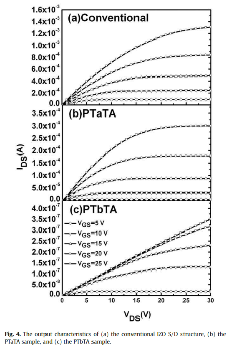
Fig. 4 shows the output characteristics of the samples. Output curves of the PTaTA sample showed fully saturated behavior for all VG similar to the conventional structure, but at the same VG voltage, the saturation VD voltage of the drain current of the PTaTA sample was slightly smaller than that of the conventional S/D structure. These saturation characteristics that appeared at a lower VD than that of the conventional S/D structure are believed to be originated from small contact resistances compared to those of the conventional S/D structure, since our suggested structure does not have heterojunctions. In contrast, the PTbTA sample showed suppressed current and non-saturation behavior for VG voltages as high as 20 V. These characteristics originated from the high sheet resistance of the sample, which obstructed carrier injection from the source electrode to the channel and from the channel to the drain.