Your browser does not fully support modern features. Please upgrade for a smoother experience.
Please note this is an old version of this entry, which may differ significantly from the current revision.
Resistive random access memory (RRAM), also often referred to as a memristor, is a non-volatile memory made from the simple structure of a metal–insulator–metal (MIM) sandwich, which is generally integrated into an elementary crossbar circuit. Resistive random access memory stands out among memory technologies due to its scalability, high-speed operation, and low power consumption.
- memristor
- resistive switching
- RRAM
1. Introduction
The last decades in human history can be called “the big data era”. Contemporary applications such as artificial intelligence, cloud storage, data mining, or the internet of things were possible due to the advances in data storage technology. Modern applications require high velocity and generate a large volume of data with less energy consumption. The conventional von Neumann architecture with silicon complementary metal-oxide-semiconductor systems (CMOS) and charge-based memory makes power scaling easier, as the charge leaks away easily in a smaller device. Therefore, non-charge-based memory technologies such as resistive random access memory (RRAM) have become promising for future applications [1][2].
Today, for data operation, both temporary and permanent storage are required. Currently, these demands are fulfilled with dynamic random access memory (DRAM), static random access memory (SRAM), and Flash memory [2]. A DRAM cell uses a capacitor to store charge and distinguish between the ‘0’ state and the ‘1’ state. The cell scaling is narrowed by the load of charge, which is accumulated in the scaled capacitor [2]. An SRAM cell stores information on the two nodes of a cross-coupled inverter pair. It is a very fast memory used to interact directly with the high-speed processor. However, an SRAM is volatile and has a lower density. Flash memories are employed for large capacity and nonvolatile requirements. A flash memory cell stores charge in the floating gate of a transistor and can store different amounts of charge to effectively store more than one bit of information per transistor [2]. All these existing charge-storage-based memory technologies face challenges in scaling down to 10 nm nodes or beyond. This is correlated with stored charge loss at the nanoscale, which results in the decrease in performance and reliability, performance, and widening of the noise margin. Furthermore, the leakage power for both SRAM and DRAM and requirements of high dynamical refresh power for DRAM pose serious design challenges [3].
Resistive random access memory (RRAM) devices have appeared as a potential candidate for the forthcoming flexible non-volatile memory (NVM) device due to their distinctive features such as scalability, higher speed operation, CMOS compatibility, and low power consumption. Therefore, in broad investigations have been carried out on RRAMs, focusing on improving their performance and eliminating limitations such as the high impact of process-induced variations [2]. Moreover, RRAM may be used in neuromorphic systems as synapse emulators [4], where one of the challenges is the lack of a compact analog RRAM that bridges the gap between the fundamental physics of the device and the behavior of the circuit/system [5].
RRAM, also often referred to as a memristor, is a non-volatile memory made from the simple structure of a metal–insulator–metal (MIM) sandwich, which is generally integrated into an elementary crossbar circuit [6][7]. Memristor is the physical realization of the fourth fundamental passive circuit element [8]. Its primary role is resistive switching. The device relies on the formation of conducting filaments to switch between low- and high-resistance states. This property makes it particularly useful for in-memory computing due to its non-volatile storage capability with a continuum of conductance states [9][10]. RRAM uses an electrical signal to activate the reversible transition between a high resistance state (HRS, OFF) and a low resistance state (LRS, ON) in a sandwiched structure, thus enabling the storage of data ‘0’ and ‘1’ [8][11][12]. Due to the characterization of the materials, the most crucial feature of MIM switches is their HRS/LRS switching ratio (the higher the ratio, the better the memristive behavior) [13].
2. RRAM Mechanism
As mentioned above, a random access memory resistor (RRAM) consists of a memory cell of resistance switching with a metal–insulator–metal structure, generally known as the MIM structure. The structure consists of a layer (I) of insulation between two metal electrodes (M) [3]. The number of electric charges flowing through it can reversibly modulate the memristor’s resistive states. The memristive device performs resistive switching behavior with an inherent memory effect. The resistive state depends both on the extra stimulations and its intrinsic states [14].
Depending on different criteria, the behavior of resistance exchange can be classified into different types. For example, resistive switching behavior can be divided into digital and analog categories based on switching dynamics. Digital resistance switches describe sudden changes between high resistance states (HRS) and low resistance states (LRS), and sudden current jumps appear in the digital cell I–V loops. Analog switching relates gradual modulation—switching cells exhibit continuous I-V loops [14]. According to the retention characteristics of the resistive states, the resistive switching behavior can be classified into volatile and non-volatile switching groups [14].
The switch from HRS to LRS is the ‘set’ process. In contrast, the LRS–HRS switch event is called a ‘reset’ process. Applying the external voltage pulse through the RRAM cell allows a transition of the device from a high resistance state (HRS), or the OFF state generally referred to as logic value ‘0’, to a low resistance state (LRS), or the ON state—logic value ‘1’ and vice versa. The resistance change phenomenon (RS) is considered the reason behind the change in resistance values in RRAM cells. In most cases, in new samples with initial resistance conditions, a voltage greater than the set voltage is required to trigger resistive switching behaviors in subsequent cycles [3][15]. To read data from the RRAM cell, a small voltage which cannot destroy the current state is applied for determination whether the cell is in the logic 0 (HRS) or logic 1 (LRS) state. Since LRS and HRS maintain their respective values even after applying voltage, RRAM is a non-volatile memory [3].
2.1. Resistive Switching
According to the current polarity, the RRAM can be divided into two modes: unipolar and bipolar (Figure 1). In unipolar switching, changing between modes does not depend on the polarity of the applied voltage. In bipolar switching, the SET and RESET processes rely on the polarity of the applied voltage. A switch from an HRS to an LRS occurs at one polarity (positive or negative) and the opposite polarity shifts the RRAM cell back into the HRS [3]. Resistance-switching properties in memristive devices were highly dependent on materials, device structures, external simulations, and switching mechanisms. Therefore, many reports deal with the adjustment of switching behavior characteristics by modifying the structure of the device and the simulation parameters [11][15].
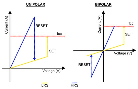
Figure 1. Unipolar and bipolar modes for RRAM devices.
The basis of a switching mechanism is the growth of a conductive filament (CF) inside the insulator. A CF is a very narrow channel that connects the top and bottom electrodes of the memory cell. Low-resistant (LRS) states with high conductivity are achieved when the filament is connected, and high-resistance state (HRS) is obtained when the filament is disconnected from the gap between the electrodes. Based on the composition of the conductive filament and the mechanism of conduction, RRAM switching can be classified as a thermal chemical mechanism (TCM), valance change mechanism (VCM), and electrochemical metallization (ECM) [3][11].
Electrochemical metallization (ECM) is based on the migration of metal ions and subsequent reduction/oxidation (redox) reactions. The junction consists of a chemically active top electrode such as Ni, Cu or Ag, a nearly inert bottom electrode (e.g., W, Pt), and a sandwiched metal oxide layer. The filament formation in such memory cells occurs due to the dissolution of the active metal electrodes, the transport of cations (M+), and their deposition or reduction on the inert electrode [3][11].
In the valence change mechanism, the formation of a conduction filament is correlated with the creation of oxygen vacancies (V2+O) and the subsequent relocation of oxygen ions (O2), thus enabling the formation of a conductive filament between the upper and lower electrodes of RRAM cell. For the commissioning of the mechanism, it is necessary to knock out oxygen atoms from the lattice by applying a high electric field toward the anode interface. The oxygen ions (O2) drift toward the electrode whereas the oxygen vacancies (V2+O) are left in the oxide layer. If noble metals are used as materials for the anode to form an interfacial oxide layer, oxygen ions (O2−) react with anode materials or are released as neutral oxygen. Next, the conductive filament (CF) is formed and the appreciable current flows in the device through the accumulation of oxygen vacancies (V2+O) in the bulk oxide, which switch the RRAM cell to the low resistance state (LRS). To return the device to the high resistance state (HRS), the reset process occurs. In the process, the oxygen ions (O2) migrate back to bulk oxide from the anode interface and combine with the oxygen vacancies (V2+O) [3][11].
The thermochemical mechanism (TCM) explains the formation and fracture of CFs resulting from ion migration induced by a thermochemical reaction (Joule heating), which is independent of the switching modes (unipolar and bipolar) for RRAM devices. In the case of LRS, the ions are driven by the Joule heating effect towards the top electrode and, in the case of the unipolar device, left oxygen vacancies. For the RESET process of the unipolar device, the current steadily increases with increasing positive voltage bias, and the formed CFs finally break when it reaches the critical temperature induced by Joule heating, which causes the device to switch back to HRS. For the RESET process of the bipolar device, oxygen ions drift back to the insulating layer due to the melting of CF and the device to HRS [11].
2.2. Activation Process
The RRAM behavior is based on the possibility of electrically modifying the conductivity of a stack of metal–insulator–metal (MIM). To activate the switching mechanism, some technologies require a preliminary formation operation [16], which is shown in Figure 2. The electroforming process (soft or hard) is usually realized by applying a large electrical bias across the two electrodes within a certain specific time interval to generate initial conductive channels via the Joule heating effect. The formation step can be conquered by appropriately modifying the fabrication process to readily introduce oxygen vacancies to facilitate the migration of anions within the switching layer [6]. Even if the forming process is performed once, this initial state plays a fundamental role in determining the subsequent array and system performance. The performance of the formation process relies on its ability to create homogeneous conductive conditions among cells, thus easing successive SET/RESET operations [16]. As explanations of the driving force of anion transport during the formation process, the following are suggested: (i) drift by electric potential gradient, (ii) electromigration assuming an electron kinetic energy, (iii) Fick diffusion due to ion concentration gradient, and (iv) thermophoresis due to temperature gradient [6].
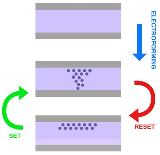
Figure 2. Process of electroforming, SET and RESET.
A standard formation can be carried out by applying a voltage ramp [17] or a voltage/current pulse to each cell individually [16]. Both formation processes produce a non-destructive soft breakdown regime and a progressive breakdown regime of the dielectric and require a sufficiently high electric field [18]. Another method, the constant voltage formation process, enables the formation of conductive filaments at lower voltages rather than the conventional fast voltage ramp method [19].
2.3. Material for Electrodes
One of the undervalued elements of MIM switches is the electrode. The materials and forms of electrodes can have a significant impact on the behavior of RS, mainly through direct participation in redox reactions or as transport routes for oxygen tanks or loading carriers [9].
Firstly, it is necessary to choose a suitable material for the top and bottom electrodes. In general, the specific material for the electrodes is related to the conduction mechanism.
VCM is triggered by the migration of field-assisted oxygen anions and valence change of the cation sublattice [20]. In the case of VCM, the most common and widely used are inert metals, such as Au, Pt, and Pd, which normally contribute less to RS, and act mainly as a carrier transport path or oxygen reservoir [9].
In the case of ECM, the conduction mechanism is based on the migration of cations in the solid electrolyte. The typical ECM cell has an asymmetric structure with one active electrode. In the case of cation-based structures, electrochemically active metals such as Cu, Ni, Ag, and Ru, have been explored [9]. Active metals with the ability to modulate the concentration or migration of anions are used, such as Ta, Ti, Al, Hf, and W. What is more, the redox reaction of a Ta electrode can lead to the formation of Ta CFs. Therefore, competition between the ECM and the VCM may exist in devices based on the Ta electrode [9]. Recently, active metals have been intentionally mixed into the electrolyte layer to achieve bipolar threshold-switching behavior with typical I–V curves. These memristive devices with bipolar threshold-changing behaviors are also called diffusive memristive devices [14].
More and more alloy electrodes are used for improving or optimizing RS behaviors by modulation of the mobile cations’ diffusivity or confination of the position of CFs [9]. The use of alloys where both components are redox-active and mobile may bring significant advantages in the design of electrode materials [21]. Most commonly used switching films are binary, ternary, or quaternary compounds such as Ta2O5, SiO2, SrTiO3, etc. In those alloys, the interactions between the ions/atoms of the active electrode/filament and the solid electrolyte matrix influence the chemical and electronic properties both of the conducting channel and also of the whole matrix [21].
Carbon-based electrodes, for example, graphene and carbon nanotubes (CNT), are reported for flexible and small-scale devices. One of the more common bottom electrodes is p- and n-type silicon, as well as nitride electrode materials such as TiN and TaN. Conducting metal oxides, such as indium tin oxide (ITO), Al-doped ZnO (AZO), Ga-doped ZnO (GZO), and F-doped SnO2 (FTO), have also been reported as electrodes for some special applications, for example, fully transparent or flexible devices [9].
The electrode material can significantly change the behavior of the active layer. Khrapovitskaya et al. [22] have investigated RS of TiO2-based memristors with respect to different material of top electrodes. In the case of the Pt electrode, the maximum to minimum resistance ratio (Roff/Ron) was up to about 100 Ω, whereas in the case of the golden electrode, the sample resistance in the low-ohmic state (Ron) was about 90 Ω, and that in the high-ohmic state (Roff) was about 900 Ω. The author claimed that the greater switching behavior in the case of memristors with gold electrodes is probably related to a lower diffusion of oxygen through the gold film compared to the case of platinum. On the other hand, Kumar et al. [23] have investigated the effect of different electrode materials in the case of the active ZnO layer of ZnO. They observed that the ZnO-based memristor with the Pt electrode showed a better hysteresis compared to Cr and Au metal electrodes. In the case of the Pt electrode, a current ratio of six times the magnitude was observed between the high resistive state and the low resistive state at 1 V, where a maximum current density value of 1.25 A/cm2 was measured.
Swathi et al. [24] investigated the changes in RS due to the bottom electrode. They investigated the Au/NiO/ITO and Au/NiO/Pt devices. Although the NiO switching layer was deposited under similar conditions, different switching patterns were observed in NiO films with ITO and Pt electrodes. In particular, the RS device with ITO as BE exhibits gradual set-and-reset switching or analog-type RS. The change from HRS to LRS and vice versa in positive and negative voltage sweeps was incremental in comparision to abrupt change in samples with Pt bottom electrode device [24].
In addition to material, the size of the top electrode influences the formation of the memristor conduction structure [25]. Gale et al. [26] showed that the scaling of the electrode changing affects the behavior of curved-type memristors and has no effect on triangular-switching ones. This suggests that the two types operate via different mechanisms. The value of the hysteresis increases with increasing electrode size as a result of the decrease in the value of Ron with increasing electrode size [26].
In another work, Gale et al. [27] observed a larger I-V curve in the case of a larger electrode, which indicates the memristor’s response under the electrical field in relation to three spatial dimensions. Furthermore, the hysteresis increases with electrode size but does not increase equally across the devices; instead, the top right quadrant of the curve increases more. This asymmetry leads to a negative hysteresis [27].
The size and materials of the electrodes may present some problems. Schroeder et al. [28] observed the molting between the top and bottom electrodes as a result of a large current during the forming process. Similarly, the fusing of electrodes lying next to each other was observed, or the observation of creating the dendritic structures on the substrates [28].
2.4. Material for Active Layer
Many thin film materials have been investigated as RS mediums for RRAM devices because of their RS characteristics under the influence of the external electrical field. Generally, organic materials and inorganic materials are two categories of RS medium [11].
2.4.1. Organic Materials
In the case of organic materials, research focuses primarily on biological materials, polymer materials, and other materials. Most of them require low-temperature processes. Therefore, in most cases, developing a way to control their interfacial pathways is a milestone [29]. For example, investigation on the memory effect began in the 1970s when the switching mechanism between different resistance states was observed in polystyrene and copper–tetracyanoquinodimethane (Cu–TNCQ) films. Since then, noteworthy progress has been made in organic memory devices [30].
Polymers are the most common group of organic materials used as active layers. One of the most commonly used materials is polyaniline (PANI). The researchers utilized its adaptive behavior: the PANI demonstrates non-linear electrical characteristics with hysteresis loop and rectification [31][32]. Berzina et al. [33] used the PANI difference in the conductivity in the oxidized and reduced states for the memristive behavior. PANI may also act as an electrode, and was utilized by Erokhin et al. [34] in a sandwich structure, where a solid electrolyte (polyethylene oxide doped with lithium salt (PEO)) acted as an active layer.
More and more researchers are focusing on producing flexible devices. For example, Xu et al. used a chlorotrifluoroethylene and vinylidene fluoride copolymer (FK-800) to produce RRAM for an artificial nociceptor (pain sensor) [35]. Another realization of a flexible memristor was proposed by Zhou [36], who used polymer nanocomposites, with the configuration of the silver nanowire (AgNW)/citric acid quantum dot (CA QD)-polyvinyl pyrrolidone (PVP)/AgNW. Park et al. [37] proposed poly(vinyl cinnamate) (PVCi) with a predefined CF.
Many polymer devices are based on complexes with 2D material or composites. One of the mediums most commonly chosen for different materials is PMMA [29][38][39] or azobenzene polymer [40].
Due to its rich electrochemical redox behavior, viologen diperchlorate EV(ClO4) with different polymers (pyridyl-iron polymer (TPy-Fe) [41], triphenylamine-containing polymer (BTPA-F) [42] are used to simulate the functions of the synapse. Other materials used in the production of memristors are (PVK (polyvinyl carbazole), PVA (polyvinyl alcohol), PDA (polydiacetylene), and PTH (polythiophene) [11].
Another widely used group of organic substances are biomaterials. Biomaterial-based memristive devices are made of biopolymers produced by organisms. These substances can be divided into two groups: carbohydrates and protein. The molecular structure of carbohydrates contains only three elements: carbon (C), hydrogen (H), and oxygen (O). However, in addition to C, H, and O, proteins usually contain nitrogen (N) from amino acids and some trace elements such as iron (Fe), zinc (Zn), copper (Cu), manganese (Mn), and so on. Thus, the memristive effect depends on trace elements, which help to form conductive filaments and redox reactions [30]. Natural organic materials can provide versatile engineering platforms and are an attractive alternative due to their biodegradability, bioabsorbability, and nontoxicity [43].
One of the most commonly used biomaterials is egg albumen [11][43]. The albumen layer is characterized by a transparency of more than 90% under visible light with a wavelength range of 230–850 nm, flexibility [30][44], clockwise and counterclockwise current hysteresis [45]. Low SET/RESET voltage ~3 V and reliable switching endurance were observed over 500 cycles with ~103 ON/OFF ratio [11].
Spider silk [46] and silkworm cocoon fibroins [11][47][48] are highly utilized in the production of MIM junctions. The fibroin structures exhibit excellent performance and behave as RRAM with the immersion process in di-isopropanol water, indicating the great potential of silk fibroin applied to transient and biocompatible electronics [11].
Battistoni et al. reported two hybrid devices based on poly(3,4-ethylenedioxy- thiophene), doped with polystyrene-sulfonate (PEDOT: PSS) and Physarum polycephalum slime mold (PP), which acted as a living electrolyte [31]. Furthermore, Abbas et al. fabricated and characterized the transparent and biocompatible resistive random access memory (ReRAM) device with the structure of Pt/Cu2+ doped salmon DNA/FTO where Cu2+ was doped in salmon DNA by solution processes [30].
Protein-based memristors were produced mainly with keratin [30] and gelatin [49]. However, polysaccharides are also widely used in the manufacture of memristors. The MIM structures are based on chitosan [30][43], cellulose [11], or glucose [11]. Furthermore, resistive switching behavior was also found in orange peel pectin [30], maple leaves [50], and anthocyanin extracted from plant tissue [51].
Organic small molecules that have a clear structure, easy purification, and low cost, and are lightweight also have caused a widespread boom in research in the field of resistive switch memory. Furthermore, in the production of RRAM, liquid crystalline polymer (LCP) aligned with polyimide was used [52]. Copper phthalocyanine nanowires were used to change the response due to IR illumination [53].
2.4.2. Inorganic Materials
Compared to organic RRAM, inorganic materials exhibit better electrical performance, more stable switching behavior, lower energy consumption, and longer retention time [11]. Hickmott proposed the first report on RS performance in binary metal oxides in 1962, which demonstrated the RS characteristics of the Al/Al2O3/Al device under the effect of an electric field [11]. Inorganic memristors usually have a typical metal–insulator–metal (MIM) structure, and their insulator layer (also known as the RS layer) is made of binary metal oxides, perovskite metal oxides, chalcogenides, and others [54].
The layer of binary metal oxides is usually formed with a single insulator such as TiO2 [11][55], NiO [11], HfO2 [11][56], SiO2 [57], TaO2 [11][58], and Ga2O3 [59]. However, with the development of research, researchers tend to make a dielectric layer diversification by doping or making a multilayer. Two or three dielectric layers have various degrees of optimization effects on the performance of the device [54]. Sakellaropoulos et al. demonstrated a comparison among other devices with three types of dielectric structures such as HfOx, TaOy/HfOx, and HfOx/TaOy/HfOx, which correspond to single-layer (SL), bilayer (BL), and triple-layer (TL) [11]. Liu et al. [54] investigated conductance modulation on TE/HfOx/AlOx/BE and Ta/TaOx/TiO2/Ti stacks. Mahata et al. reported an RRAM device with ALD-based HfO2/Al2O3 stack layers, which exhibited excellent performance with an operating voltage lower than ~2 V and an ON/OFF ratio [11]. Prezioso et al. investigated spike time-dependent plasticity on 200-nm Al2O3/TiO2−x memristors integrated into 12 × 12 crossbars [60].
For a memristive performance, porous bionic structures are investigated. One of the best examples is the work of Gao et al. [61], who researched a double-layer structure comprising a Pt/porous LiCoO2/porous SiO2/Si stack. Furthermore, binary oxides are mixed with nanomaterials such as nanotubes, which may increase reservoir oxygen vacancies [11].
Another group of materials that are used is perovskites. Perovskite is a compound with the ABX3 type crystal. A is a monovalent cation and can be an organic (methylammonium CH3NH3+) or inorganic (Cs+) cation. B is a divalent cation, such as Pb2+, and Sn2+, and X is an anion. When X is oxygen (O), the material is called an oxide perovskite, and when X is a halide (I or Br), it is called an HP [62]. The oxide perovskite, which was investigated, had higher dielectric constants, and those are LaAlO3, SrTiO3, Pr0.7Ca0.3MnO3, and BiFeO3 [11]. Halide perovskite (HP) materials with point defects (such as gaps, vacancies, and inversions) also have a strong application potential in memristors with an averaged ON/OFF ratio of 104–105 [62][63]. Unfortunately, most HPs are lead-based: MAPbI3, FAPbI3, HC(NH2)2PbI3, CsPbI3, or (Cs3Bi2I9)x- (CsPbI3)1−x. Thus, the thermal instability and toxicity severely restricted their further practical applications. Therefore, more and more researchers are focusing on lead-free HP such as CsSnI3, Cs3Bi2I9, (MA)3Bi2I9, (BzA)2CuBr4, or CsBi3I10 [64][65].
Organic–inorganic halide perovskites (OHPs) have gained attention as promising materials for memristors. Particulary, their mixed ionic-electronic conduction ability paired with light sensitivity allows OHPs to show novel functions such as optical erase memory, optogenetics-inspired synaptic functions, and light-accelerated learning capability [66]. Furthermore, to enhance the properties of perovskites, the material is mixed with nanostructures, for example, reduced graphene oxide (rGO) [67]. In addition, amorphous perovskite materials exhibit memristive properties [68].
A series of 2D materials such as graphene and molybdenum disulfide (disulfide perovskite) have gained popularity due to their small size, ultrathinness, and excellent physical properties, which have resulted in the performance of RRAM devices [11]. For example, additional graphene layers can act as the charge storage medium, resulting in a higher retention time. In addition, graphene can offer increased transparency, light weight, flexibility, and low sheet resistance [13]. Nonvolatile and bistable memory devices based on graphene oxide (GO) have prompted great interest due to their high optical transparency, low cost, easy fabrication, high flexibility, environmentally friendly nature, and controllable chemical and physical properties for future electronic devices [13]. On the other hand, MoS2 embedded in the active layer tends to trap and release charge carriers [13].
This entry is adapted from the peer-reviewed paper 10.3390/cryst13030416
References
- Carlos, E.; Branquinho, R.; Martins, R.; Kiazadeh, A.; Fortunato, E. Recent Progress in Solution-Based Metal Oxide Resistive Switching Devices. Adv. Mater. 2021, 33, 2004328.
- Gupta, V.; Kapur, S.; Saurabh, S.; Grover, A. Resistive Random Access Memory: A Review of Device Challenges. IEEE Trans. Electron Devices 2020, 37, 377–390.
- Zahoor, F.; Azni Zulkifli, T.Z.; Khanday, F.A. Resistive Random Access Memory (RRAM): An Overview of Materials, Switching Mechanism, Performance, Multilevel Cell (Mlc) Storage, Modeling, and Applications. Nanoscale Res. Lett. 2020, 15, 90.
- Mahata, C.; Park, J.; Ismail, M.; Kim, D.H.; Kim, S. Improved Resistive Switching with Low-Power Synaptic Behaviors of ZnO/Al2O3 Bilayer Structure. Materials 2022, 15, 6663.
- Liao, Y.; Gao, B.; Xu, F.; Yao, P.; Chen, J.; Zhang, W.; Tang, J.; Wu, H.; Qian, H. A Compact Model of Analog RRAM with Device and Array Nonideal Effects for Neuromorphic Systems. IEEE Trans. Electron Devices 2020, 67, 1593–1599.
- Mohammad, B.; Jaoude, M.A.; Kumar, V.; Al Homouz, D.M.; Nahla, H.A.; Al-Qutayri, M.; Christoforou, N. State of the Art of Metal Oxide Memristor Devices. Nanotechnol. Rev. 2016, 5, 311–329.
- Fauzi, F.B.; Ani, M.H.; Herman, S.H.; Mohamed, M.A. Dilute Electrodeposition of TiO2 and ZnO Thin Film Memristors on Cu Substrate. IOP Conf. Ser. Mater. Sci. Eng. 2018, 340, 012006.
- Hu, W.; Yang, B.; Zhang, Y.; She, Y. Recent Progress in Physically Transient Resistive Switching Memory. J. Mater. Chem. C Mater. 2020, 8, 14695–14710.
- Shi, T.; Wang, R.; Wu, Z.; Sun, Y.; An, J.; Liu, Q. A Review of Resistive Switching Devices: Performance Improvement, Characterization, and Applications. Small Struct. 2021, 2, 2000109.
- Anonymous. Beyond von Neumann. Nat. Nanotechnol. 2020, 15, 507.
- Shen, Z.; Zhao, C.; Qi, Y.; Xu, W.; Liu, Y.; Mitrovic, I.Z.; Yang, L.; Zhao, C. Advances of RRAM Devices: Resistive Switching Mechanisms, Materials and Bionic Synaptic Application. Nanomaterials 2020, 10, 1437.
- Yu, S.; Lee, B.; Wong, H.-S.P. Metal Oxide Resistive Switching Memory. In Springer Series in Materials Science; Springer: Berlin, Germany, 2012; Volume 149, pp. 303–335. ISBN 9781441999306.
- Rehman, M.M.; Rehman, H.M.M.U.; Gul, J.Z.; Kim, W.Y.; Karimov, K.S.; Ahmed, N. Decade of 2D-Materials-Based RRAM Devices: A Review. Sci. Technol. Adv. Mater. 2020, 21, 147–186.
- Yang, R. Review of Resistive Switching Mechanisms for Memristive Neuromorphic Devices. Chin. Phys. B 2020, 29, 094305.
- Wong, H.S.P.; Lee, H.Y.; Yu, S.; Chen, Y.S.; Wu, Y.; Chen, P.S.; Lee, B.; Chen, F.T.; Tsai, M.J. Metal-Oxide RRAM. Proc. IEEE 2012, 100, 1951–1970.
- Grossi, A.; Zambelli, C.; Olivo, P.; Miranda, E.; Stikanov, V.; Walczyk, C.; Wenger, C. Electrical Characterization and Modeling of Pulse-Based Forming Techniques in RRAM Arrays. Solid State Electron. 2016, 115, 17–25.
- Snyder, E.S.; Suehle, J. Detecting Breakdown in Ultra-Thin Dielectrics Using a Fast Voltage Ramp. In Proceedings of the 1999 IEEE International Integrated Reliability Workshop Final Report (Cat. No. 99TH8460), Lake Tahoe, CA, USA, 18–21 October 1999; pp. 118–123.
- Grossi, A.; Walczyk, D.; Zambelli, C.; Miranda, E.; Olivo, P.; Stikanov, V.; Feriani, A.; Sune, J.; Schoof, G.; Kraemer, R.; et al. Impact of Intercell and Intracell Variability on Forming and Switching Parameters in RRAM Arrays. IEEE Trans. Electron Devices 2015, 62, 2502–2509.
- Kalantarian, A.; Bersuker, G.; Gilmer, D.C.; Veksler, D.; Butcher, B.; Padovani, A.; Pirrotta, O.; Larcher, L.; Geer, R.; Nishi, Y.; et al. Controlling Uniformity of RRAM Characteristics through the Forming Process. In Proceedings of the 2012 IEEE International Reliability Physics Symposium (IRPS), Anaheim, CA, USA, 15–19 April 2012; pp. 3–7.
- Lim, E.W.; Ismail, R. Conduction Mechanism of Valence Change Resistive Switching Memory: A Survey. Electronics 2015, 4, 586–613.
- Valov, I.; Yang, Y. Memristors with Alloyed Electrodes. Nat. Nanotechnol. 2020, 15, 510–511.
- Khrapovitskaya, Y.V.; Maslova, N.E.; Grishchenko, Y.V.; Demin, V.A.; Zanaveskin, M.L. The Effect of the Memristor Electrode Material on Its Resistance to Degradation under Conditions of Cyclic Switching. Tech. Phys. Lett. 2014, 40, 317–319.
- Kumar, A.; Baghini, M.S. Experimental Study for Selection of Electrode Material for ZnO-Based Memristors. Electron. Lett. 2014, 50, 1547–1549.
- Swathi, S.P.; Angappane, S. Digital and Analog Resistive Switching in NiO-Based Memristor by Electrode Engineering. Jpn. J. Appl. Phys. 2022, 61, SM1009.
- Avilov, V.I.; Kolomiytsev, A.S.; Tominov, R.V.; Alyabyeva, N.I.; Bykova, E.M. Investigation of the Electrode Material Influence on the Titanium Oxide Nanosize Structures Memristor Effect. J. Phys. Conf. Ser. 2018, 1124, 022019.
- Gale, E.; De Lacy Costello, B.; Adamatzky, A. The Effect of Electrode Size on Memristor Properties: An Experimental and Theoretical Study. In Proceedings of the2012 IEEE International Conference on Electronics Design, Systems and Applications (ICEDSA), Kuala Lumpur, Malaysia, 5–6 November 2012; pp. 80–85.
- Gale, E.M.; Costello, B.D.L.; Adamatzky, A. Which Memristor Theory Is Best for Relating Devices Properties to Memristive Function? arXiv 2013, arXiv:1312.4422.
- Schroeder, H.; Pandian, R.; Miao, J. Resistive Switching and Changes in Microstructure. Phys. Status Solidi (A) Appl. Mater. Sci. 2011, 208, 300–316.
- Lee, S.H.; Park, H.L.; Kim, M.H.; Kang, S.; Lee, S.D. Interfacial Triggering of Conductive Filament Growth in Organic Flexible Memristor for High Reliability and Uniformity. ACS Appl. Mater. Interfaces 2019, 11, 30108–30115.
- Sun, B.; Zhou, G.; Guo, T.; Zhou, Y.N.; Wu, Y.A. Biomemristors as the next Generation Bioelectronics. Nano Energy 2020, 75, 104938.
- Battistoni, S.; Dimonte, A.; Erokhin, V. Organic Memristor Based Elements for Bio-Inspired Computing. In Advances in Unconventional Computing. Emergence, Complexity and Computation; Springer: Cham, Switzerland, 2017; pp. 469–496.
- Berzina, T.; Erokhina, S.; Camorani, P.; Konovalov, O.; Erokhin, V.; Fontana, M.P. Electrochemical Control of the Conductivity in an Organic Memristor: A Time-Resolved X-Ray Fluorescence Study of Ionic Drift as a Function of the Applied Voltage. ACS Appl. Mater. Interfaces 2009, 1, 2115–2118.
- Berzina, T.; Smerieri, A.; Bernab, M.; Pucci, A.; Ruggeri, G.; Erokhin, V.; Fontana, M.P. Optimization of an Organic Memristor as an Adaptive Memory Element. J. Appl. Phys. 2009, 105, 124515.
- Erokhin, V.; Howard, G.D.; Adamatzky, A. Organic Memristor Devices for Logic Elements with Memory. Int. J. Bifurc. Chaos 2012, 22, 1–9.
- Xu, X.; Cho, E.J.; Bekker, L.; Talin, A.A.; Lee, E.; Pascall, A.J.; Worsley, M.A.; Zhou, J.; Cook, C.C.; Kuntz, J.D.; et al. A Bioinspired Artificial Injury Response System Based on a Robust Polymer Memristor to Mimic a Sense of Pain, Sign of Injury, and Healing. Adv. Sci. 2022, 9, 629.
- Zhou, Z.; Mao, H.; Wang, X.; Sun, T.; Chang, Q.; Chen, Y.; Xiu, F.; Liu, Z.; Liu, J.; Huang, W. Transient and Flexible Polymer Memristors Utilizing Full-Solution Processed Polymer Nanocomposites. Nanoscale 2018, 10, 14824–14829.
- Park, H.L.; Kim, M.H.; Kim, M.H.; Lee, S.H. Reliable Organic Memristors for Neuromorphic Computing by Predefining a Localized Ion-Migration Path in Crosslinkable Polymer. Nanoscale 2020, 12, 22502–22510.
- Lee, S.H.; Park, H.L.; Keum, C.M.; Lee, I.H.; Kim, M.H.; Lee, S.D. Organic Flexible Memristor with Reduced Operating Voltage and High Stability by Interfacial Control of Conductive Filament Growth. Phys. Status Solidi Rapid Res. Lett. 2019, 13, 1900044.
- Park, H.L.; Lee, T.W. Organic and Perovskite Memristors for Neuromorphic Computing. Org. Electron. 2021, 98, 106301.
- Jaafar, A.H.; Al Chawa, M.M.; Cheng, F.; Kelly, S.M.; Picos, R.; Tetzlaff, R.; Kemp, N.T. Polymer/TiO2Nanorod Nanocomposite Optical Memristor Device. J. Phys. Chem. C 2021, 125, 14965–14973.
- Yang, X.; Wang, C.; Shang, J.; Zhang, C.; Tan, H.; Yi, X.; Pan, L.; Zhang, W.; Fan, F.; Liu, Y.; et al. An Organic Terpyridyl-Iron Polymer Based Memristor for Synaptic Plasticity and Learning Behavior Simulation. RSC Adv. 2016, 6, 25179–25184.
- Liu, G.; Wang, C.; Zhang, W.; Pan, L.; Zhang, C.; Yang, X.; Fan, F.; Chen, Y.; Li, R.W. Organic Biomimicking Memristor for Information Storage and Processing Applications. Adv. Electron. Mater. 2016, 2, 1500298.
- Min, S.Y.; Cho, W.J. Memristive Switching Characteristics in Biomaterial Chitosan-Based Solid Polymer Electrolyte for Artificial Synapse. Int. J. Mol. Sci. 2021, 22, 773.
- Yan, X.; Li, X.; Zhou, Z.; Zhao, J.; Wang, H.; Wang, J.; Zhang, L.; Ren, D.; Zhang, X.; Chen, J.; et al. Flexible Transparent Organic Artificial Synapse Based on the Tungsten/Egg Albumen/Indium Tin Oxide/Polyethylene Terephthalate Memristor. ACS Appl. Mater. Interfaces 2019, 11, 18654–18661.
- Tan, M.T.; Wang, T.; Gao, X.; Zhong, Y.N.; Zhang, J.Y.; Xu, J.L.; Li, C.; Wang, S.D. Egg-White-Based Polymer Memristors with Competing Electronic-Ionic Effect and Timescale-Dependent Current Modulation. IEEE Electron. Device Lett. 2021, 42, 228–231.
- Sun, B.; Liang, D.; Li, X.; Chen, P. Nonvolatile Bio-Memristor Fabricated with Natural Bio-Materials from Spider Silk. J. Mater. Sci. Mater. Electron. 2016, 27, 3957–3962.
- Hota, M.K.; Bera, M.K.; Kundu, B.; Kundu, S.C.; Maiti, C.K. A Natural Silk Fibroin Protein-Based Transparent Bio-Memristor. Adv. Funct. Mater. 2012, 22, 4493–4499.
- Wang, J.; Shi, C.; Sushko, M.L.; Lan, J.; Sun, K.; Zhao, J.; Liu, X.; Yan, X. Boost of the Bio-Memristor Performance for Artificial Electronic Synapses by Surface Reconstruction. ACS Appl. Mater. Interfaces 2021, 13, 39641–39651.
- Ge, L.; Xuan, W.; Liu, S.; Huang, S.; Wang, X.; Dong, S.; Jin, H.; Luo, J. Biomaterial Gelatin Film Based Crossbar Structure Resistive Switching Devices. IEEE Trans. Nanotechnol. 2018, 17, 78–83.
- Ranjan, S. TiO2 and Biomaterials Based Memristor Devices and Its In-Memory Computing Applications; University of Waterloo: Waterloo, ON, USA, 2020.
- Sun, B.; Guo, T.; Zhou, G.; Wu, J.; Chen, Y.; Zhou, Y.N.; Wu, Y.A. A Battery-Like Self-Selecting Biomemristor from Earth-Abundant Natural Biomaterials. ACS Appl. Bio Mater. 2021, 4, 1976–1985.
- Park, H.L.; Kim, M.H.; Lee, S.H. Control of Conductive Filament Growth in Flexible Organic Memristor by Polymer Alignment. Org. Electron. 2020, 87, 105927.
- Lv, Z.; Hu, Q.; Xu, Z.X.; Wang, J.; Chen, Z.; Wang, Y.; Chen, M.; Zhou, K.; Zhou, Y.; Han, S.T. Organic Memristor Utilizing Copper Phthalocyanine Nanowires with Infrared Response and Cation Regulating Properties. Adv. Electron. Mater. 2019, 5, 1–9.
- Liu, H.; Wei, M.; Chen, Y. Optimization of Non-Linear Conductance Modulation Based on Metal Oxide Memristors. Nanotechnol. Rev. 2018, 7, 443–468.
- Gergel-Hackett, N.; Hamadani, B.; Dunlap, B.; Suehle, J.; Richter, C.; Hacker, C.; Gundlach, D. A Flexible Solution-Processed Memristor. IEEE Electron Device Lett. 2009, 30, 706–708.
- Amer, S.; Sayyaparaju, S.; Rose, G.S.; Beckmann, K.; Cady, N.C. A Practical Hafnium-Oxide Memristor Model Suitable for Circuit Design and Simulation. In Proceedings of the 2017 IEEE International Symposium on Circuits and Systems (ISCAS), Baltimore, MD, USA, 28–31 May 2017.
- Mikhaylov, A.N.; Belov, A.I.; Guseinov, D.V.; Korolev, D.S.; Antonov, I.N.; Efimovykh, D.V.; Tikhov, S.V.; Kasatkin, A.P.; Gorshkov, O.N.; Tetelbaum, D.I.; et al. Bipolar Resistive Switching and Charge Transport in Silicon Oxide Memristor. Mater. Sci. Eng. B Solid State Mater. Adv. Technol. 2015, 194, 48–54.
- Strachan, J.P.; Torrezan, A.C.; Miao, F.; Pickett, M.D.; Joshua Yang, J.; Yi, W.; Medeiros-Ribeiro, G.; Stanley Williams, R. State Dynamics and Modeling of Tantalum Oxide Memristors. IEEE Trans. Electron Devices 2013, 60, 2194–2202.
- Wang, S.; He, C.; Tang, J.; Yang, R.; Shi, D.; Zhang, G. Electronic Synapses Based on Ultrathin Quasi-Two-Dimensional Gallium Oxide Memristor. Chin. Phys. B 2019, 28, 017304.
- Prezioso, M.; Merrikh Bayat, F.; Hoskins, B.; Likharev, K.; Strukov, D. Self-Adaptive Spike-Time-Dependent Plasticity of Metal-Oxide Memristors. Sci. Rep. 2016, 6, 2–7.
- Gao, Q.; Huang, A.; Zhang, J.; Ji, Y.; Zhang, J.; Chen, X.; Geng, X.; Hu, Q.; Wang, M.; Xiao, Z.; et al. Artificial Synapses with a Sponge-like Double-Layer Porous Oxide Memristor. NPG Asia Mater. 2021, 13, 3.
- Cao, G.; Cao, G.; Cheng, C.; Zhang, H.; Zhang, H.; Chen, R.; Huang, B.; Yan, X.; Pei, W.; Chen, H.; et al. The Application of Halide Perovskites in Memristors. J. Semicond. 2020, 41, 051205.
- Xiao, X.; Hu, J.; Tang, S.; Yan, K.; Gao, B.; Chen, H.; Zou, D. Recent Advances in Halide Perovskite Memristors: Materials, Structures, Mechanisms, and Applications. Adv. Mater. Technol. 2020, 5, 1900914.
- Zeng, F.; Guo, Y.; Hu, W.; Tan, Y.; Zhang, X.; Feng, J.; Tang, X. Opportunity of the Lead-Free All-Inorganic Cs 3 Cu 2 I 5 Perovskite Film for Memristor and Neuromorphic Computing Applications. ACS Appl. Mater. Interfaces 2020, 12, 23094–23101.
- Fang, Y.; Zhai, S.; Chu, L.; Zhong, J. Advances in Halide Perovskite Memristor from Lead-Based to Lead-Free Materials. ACS Appl. Mater. Interfaces 2021, 13, 17141–17157.
- Zhao, X.; Xu, H.; Wang, Z.; Lin, Y.; Liu, Y. Memristors with Organic-Inorganic Halide Perovskites. InfoMat 2019, 1, 183–210.
- Kumari, K.; Majumder, S.; Thakur, A.D.; Ray, S.J. Temperature-Dependent Resistive Switching Behaviour of an Oxide Memristor. Mater. Lett. 2021, 303, 130451.
- Nili, H.; Walia, S.; Balendhran, S.; Strukov, D.B.; Bhaskaran, M.; Sriram, S. Nanoscale Resistive Switching in Amorphous Perovskite Oxide (a- SrTiO3) Memristors. Adv. Funct. Mater. 2014, 24, 6741–6750.
This entry is offline, you can click here to edit this entry!