Your browser does not fully support modern features. Please upgrade for a smoother experience.
Please note this is an old version of this entry, which may differ significantly from the current revision.
The functional layer is an important part of the storage mechanism in lithium-ion batteries, as it helps to improve the performance and stability of the interface and allows for the efficient transfer of ions and electrons. The film deposition techniques are vital for the development of lithium-ion batteries by providing a functional layer at the interface between electrode and electrolyte, which fabricates a solid-state battery with a different approach from the traditional methods.
- lithium-ion batteries
- coating
- sputtering
- pulsed laser deposition
- chemical vapor deposition
- atomic layer deposition
- solid-state battery
1. Introduction
The functional layer is an important part of the storage mechanism in lithium-ion batteries, as it helps to improve the performance and stability of the interface and allows for the efficient transfer of ions and electrons. The film deposition techniques are vital for the development of lithium-ion batteries by providing a functional layer at the interface between electrode and electrolyte, which fabricates a solid-state battery with a different approach from the traditional methods.
2. Physical Vapor Deposition
Physical Vapor Deposition (PVD) techniques can help in surface modification by changing the physical properties of the surface. PVD is a process that involves the deposition of a thin film onto a substrate. PVD techniques can change the physical properties of the surface by altering its composition, structure, or morphology. In the case of lithium-ion batteries, PVD can be used to deposit a thin film of a conductive material, such as a metal or metal oxide, onto the electrode surface to improve its electronic conductivity and reduce its impedance. During PVD, target material was emitted through an energy supply with the form of heat, pulsed laser, and protons subsequently traveled in a controlled environment, then condensed on a substrate. The deposition rate and film properties are influenced by a range of processing factors including power density, chamber atmosphere, vacuum degree, gas pressure, target-substrate distance, and substrate temperature. With their excellent film-forming quality in a relatively short time, this section selectively introduces common magnetron sputtering and pulsed laser deposition techniques. It is undeniable that other PVD techniques such as thermal evaporation made a great contribution to the field of lithium-ion batteries [1][2]. However, restricted by the disadvantages of thermal evaporation, there are limited works have been reported for the modification of lithium-ion batteries. For example, many alloys and combinations are difficult to deposit due to the different melting points. The deposited film is less uniform at several nanometers of thickness and has less controllable variables [3].
2.1. Magnetron Sputtering
Direct current (DC) and radio frequency (RF) magnetron sputtering (MS) are effective techniques for surface engineering because they allow for precise control of the film thickness, composition, and microstructure. Magnetron sputtering was first observed as the loss of cathode material in a glow discharge device by Grove in 1852 [4]. In this process, the surface of the target is eroded by particle bombardment through high voltage and then landed on the substrate after traveling in the chamber for a while. The presence of a magnetic field facilitates the generation of Ar+ and further inhibits the heat up of substrate via controlling secondary electrons moving circularly around the target. Therefore, the whole process includes [5][6]: ① generation of Ar+, ② bombardment of Ar+ toward the target by electric field acceleration, ③ escapement of target particle from the surface, ④ film formation when in contact with the substrate.
It is worth noting that a wide range of materials could be sputtered regardless of conductivity. High conductive targets such as metal or alloy sputtered by DC MS, while the sputtering of insulators and semiconductors is realized by RF MS. For example, ceramic with low conductivity would be sputtered under RF sputtering [7]. The choice of materials for individual processes is typically driven by the specific properties of the material being deposited. The choice of materials for individual processes is typically driven by the specific properties of the deposited material. In the case of lithium-ion batteries, the choice of material for surface modification is often driven by the need to improve the performance and stability of the electrode-electrolyte interface, which may require the deposition of a conductive or protective film.
Sputtering techniques facilitate the investigation of the battery with the fabrication of a binder-free electrode for a thin-film battery or modification of the electrode/electrolyte in lithium-ion batteries. The deposition rate of magnetron sputtering is generally 1–10 nm/s [8], which is mainly related to the parameters of equipment operation such as chamber pressure, the distance between target and substrate, etc. Additionally, the film properties can be tuned by varying deposition parameters such as substrate temperature, power, time, working pressure, etc. Compared to other film deposition methods, sputtering is characterized by several remarkable advantages and disadvantages [9]:
Advantages
First, the sputtering process can be achieved at low temperatures, which is friendly for flexible substrates. The rigid substrates can be heated to promote deeper diffusion of the particles and provide additional energy for bonding with the substrate [10][11]. Second, sputtering enables good adhesion of films on substrates due to the highly energetic collision with accelerating speed via transforming kinetic energy into binding force partially [12]. Third, the ability of stoichiometric transfer enables the same composition of target and as-deposited film [13][14]. Fourth, the deposition rate is mainly controlled by a power supply, while a faster deposition rate can sometimes be achieved at high power [15]. Fifth, sputtering provides the possibility for scalable fabrication from laboratory up to industrial scale, with the ability to exactly control sputtering parameters (deposition rate(1–10 nm/s), uniformity, particle size) [16]. In industry, sputtering is favorable for its easy working mechanism and reproducible film deposition on a large scale.
Disadvantages
Low availability of target: circle groove would be formed in the surface of the target and would be deeper after a long period of utilization due to secondary electron damage, which in turn resulted in irreversible usage [17].
2.2. Pulsed Laser Deposition
As a most promising PVD technique, the energy of pulsed laser deposition (PLD) was supplied from laser pulses and focused on a target leading to material melting, evaporation, and ionization [18]. This produces a plasma plume that expands rapidly away from the target surface. The ablated material is collected on a substrate upon which it condenses and forms a thin film with a deposition rate of 0.03–0.07 nm/pulse [1]. Reasonably, the PLD process can be divided into three steps [19][20]: ① the generation of plasma, ② expansion of plasma plume, ③ nucleation of vapor and film growth.
The commonly used lasers include Nd: YAG (Neodymium-doped Yttrium Aluminum Garnet, λ = 266 nm), ArF (λ = 193 nm), and KrF (λ = 248 nm), while the mean diameter of the particle would increase with wavelength [21]. During the deposition, the film growth rate is controlled by the pulsing duration of the laser [18]. The deposition rate will increase when employing high repetition and high-power lasers [22]. When depositing lithium-containing material, excess lithium is required due to the high vapor pressure of lithium and its easy scattering character during deposition [23]. During the PLD process, depositing conditions such as gas pressure, deposition temperature, laser power, and post-annealing process all influence the morphology, structure, and consequent properties (e.g., electrical and ion conductivities) of the films [24].
To summarize, activated by laser energy, the plasma including ions, electrons, and atoms is ejected from the target surface forming glow zones with high temperature, which in turn provide enough energy for melting and evaporating of the target material to the vapor phase. The availability of various experimental parameters permits film growth in a wide range of characteristics. Accordingly, film characteristics such as epitaxy, phase purity, density, roughness, morphology, composition, and thickness would be tuned. Furthermore, both the substrate and target were rotated to promise uniform deposition, and the laser beam was scanned to avoid the puncture of the target. The main difference in the working mechanism between sputtering and pulsed laser deposition was the type of supplied energy as well as the mechanism of vapor generation. Namely, it can be considered that the velocity energy of plasma is transferred to the target during sputtering and the heat of laser irradiation induce vaporization of the target in PLD. Subsequently, as a PVD technique, pulsed laser deposition resembles sputtering in many aspects. In this configuration, the characteristic of pulsed laser deposition was briefly introduced in comparative perspectives as follows.
Advantages
Firstly, the high energy supplied by laser pulse may enable film crystallization during a deposition without post-annealing (e.g., a strong temperature gradient leads to the formation of amorphous-crystalline core-shell silicon nanostructures at room temperature) [25]. Secondly, PLD has been considered a clean deposition method without introducing precursor into the chamber [26]. Correspondingly, the high energy from the laser enables stoichiometry transfer from the localized target without chamber contamination. Additionally, the in-situ introduction of reaction gas allowed the formation of the heteroepitaxial film [27].
Disadvantages
In contrast to sputtering, compactness and adhesion of film were inferior due to the lower kinetic energy in the PLD process. Besides, the PLD possesses a lower deposition rate, due to the deposition rate being proportional to laser power, frequency, and fluency [22].
Notably, the introduction of reactive gas (O2 or N2) in the chamber is an alternative approach toward depositing a composite film, which was called reactive deposition [28][29]. The vaporized target particles would react with gas to form a compound, which may enable elemental doping. Additionally, deposition from multi-target in one chamber was observed with the rotation of substrate for uniform film deposition [30]. For instance, a solid electrolyte with multi-element was deposited by alternative sputtering of Al, Li2O, and LLZO (Li7La3Zr2O12) target [31]. Normally, an excessive amount of lithium was added to the target to compensate for lithium loss during sputtering [32]. Besides, the nitrogen-doped carbon was enabled by bombarding graphite targets in the nitrogen atmosphere [33].
Despite the numerous advantages of the physical vapor deposition process, it also shows disadvantages in practical application. PLD and MS need targets with a suitable diameter and an optimized composition. Additionally, if the chamber is not under a high vacuum, prepared films may be contaminated. More seriously, due to the line-of-sight deposition feature, vapor particles hardly attach to the inner side of a porous structure. It is also difficult to deposit film in the “shadow” area of the uneven surface with pinholes generated during deposition. To compensate for the disadvantage of PVD techniques, the reactive vapor reaction process was often conducted to make a wide range of usage.
3. Reactive Vapor Deposition
To differentiate and unify the chemical vapor deposition (CVD) and atomic layer deposition (ALD) processes, here, they are called reactive vapor deposition (RVD). The RVD process would be witnessing the breaking and binding of chemical bonds excited by supplied energy and forming a new material, which is the main difference from PVD. Another divergence of RVD should be the non-line of sight deposition feature derived from the pervading ability of vapor phase precursor in pores and voids mixed in a carrier gas [34]. Activation energy is required in the reaction process for bond breaking and linking with the form of heat, photons, and plasma [35][36][37]. Correspondingly, low-temperature deposition is possible in the vapor reaction process assisted by plasma [38][39].
3.1. Chemical Vapor Deposition
In the CVD process, reactions are conducted in a quartz tube with the favor of carrier gas in higher temperatures (200–1100 °C) [40][41][42]. Whereas, the ultrahigh temperature (>2000 °C) is adopted for the growth of certain materials [43]. Notably, a wide range of materials can be synthesized with various morphology. For example, a two-dimensional material with a monolayer or few layers would be realized by CVD, such as graphene, MoS2, and PtSe [44][45][46]. There are several processes involved in CVD [47][48]: ① The precursor in a vapor state was dispersed and adhered onto the surface of a substrate with the aid of carrier gas. ② The precursor decomposed into a smaller unit to react with the substrate and then form a thin film. ③ The gas-phase byproduct was purged by a vacuum pump. The precursor can be solid-state placed at the entrance of carrier gas or gas phase would adhere at the substrate followed by carrier gas from solid precursor placed at the entrance of carrier gas or gas phase filled in a bottle. The coating can be conducted at both the smooth silicon substrate and three-dimensional framework [49][50]. Affected by the chemical reaction rate of different film deposition, equipment models, and other factors, the CVD deposition rate is generally 1–100 nm/s [51]. Film thickness can be controlled by tuning physical parameters such as gas flow, temperature, and reaction time.
Advantages
The complex-structured substrate with pores and voids can be coated due to the vapor precursor can spread into them mixed in a carrier gas, which is the main difference between PVD and RVD.
Disadvantages
The major disadvantage of CVD is stemmed from its slow deposition rate. Another disadvantage is associated with the toxicity or flammability nature of precursor or exhausted gas. Additionally, a higher temperature is required to vaporize the precursor from a solid/liquid state. However, sometimes, the required energy can be lowered through the introduction of a laser or initiator [52].
3.2. Atomic Layer Deposition
ALD has been demonstrated to be an effective method to either synthesize electrode/electrolyte materials for micro/thin-film batteries or modify particles and electrodes/electrolytes through depositing thin film in a layer-by-layer process based on the sequential and saturated reaction of gaseous precursors with a cyclic manner [53]. Attributing to the limited number of active sites in the as-depositing substrate, reactive gas remained for seconds to react entirely (saturatively) when reactive gas entered into the reaction chamber, then the redundant reactive gas and by-product will be purged away by a carrier gas (N2). In the ALD process, one cycle also consists of four steps [54]: ① Release precursor in the reaction chamber, ② Purge away excess precursors and byproducts through carrier gas, ③ Exposure of a second precursor, ④ Evacuation of the excess precursor and byproduct. The desired film thickness is often realized by the controlling cycle number as well as deposition time (about 0.1 nm film was deposited in one cycle).
Advantages
Despite the similar point of the CVD process in conformal deposition, ALD possesses self-limiting nature due to its limited active sites and precursor in each cycle, resulting in thin films with uniform and controlled thickness. Additionally, the film thickness can be exactly controlled on the atomic scale with a low deposition rate of few angstroms in each cycle, which provides precise control over the film thickness, resulting in uniform and conformal thin films. Meanwhile, ALD requires a lower reaction temperature (100–300 °C) than the CVD process, while the lower temperature sacrificed the reaction rate as well as film growth. Higher temperatures (above 300 °C) compromise the growth rate since the rapid decomposition of precursors. Notably, gas-phase precursors enable penetration of pores, voids, and grain boundaries of the target material.
Disadvantages
It is suffered from a low deposition rate with few angstroms in one cycle. Moreover, few materials can be deposited through ALD the process due to the limited choice of precursors.
Therefore, RVD enables excellent step coverage on high aspect ratio structures. The reasonably, uniform and dense thin film would be achieved attributed to the smaller participating unit down to molecule size. Consequently, RVD is seldom applied in the fabrication of thin-film batteries restricted by the low deposition rate. However, it is commonly observed that the coating of the electrode surface with a functional layer and the formation of the electrode is assisted by a sacrificial template. In an endeavor to obtain full coverage with uniform coating on powder, researchers introduce fluidized beds in the film deposition process [55][56]. This method of rationally matching the required modules into advanced thin film deposition equipment provides a new idea for the next generation of industrial production of lithium-ion batteries coated with functional thin films. Here outlines the main characteristics of as-discussed four types of deposition techniques (Figure 1). It is not difficult to find that these methods have their own advantages and disadvantages as well as corresponding restrictions. From a practical point of view, researchers need to use functional thin films to compensate for the shortcomings of existing electrodes, in an attempt to obtain more comprehensive and excellent material properties. Kotlarski et al. [57] found that W deposited on aluminum and copper surfaces exhibited α-W and β-W, respectively. Among them, the resistivity of β-W is much higher than that of α-W, and the β-W can be changed into α-W after thermal annealing treatment. Under the condition of applying a contact pressure of 40 N after depositing a thickness W of 6 um, the contact resistance value of the aluminum material decreased from 9 to 6 mΩ, and the contact resistance of copper increased from 0.12 to 0.65 mΩ. Furthermore, the anti-corrosion ability of the film after the deposition of W has been improved, and the performance of α-W is better than that of β-W [58]. Certainly, in addition to the characteristics of the deposited material itself, the quality of the film obtained after deposition is also crucial to the electrode. Parameters such as adhesion, crystal phase of film materials, impurity content, and roughness are often related to factors such as deposition method, deposition environment, and sample surface cleanliness [59][60].
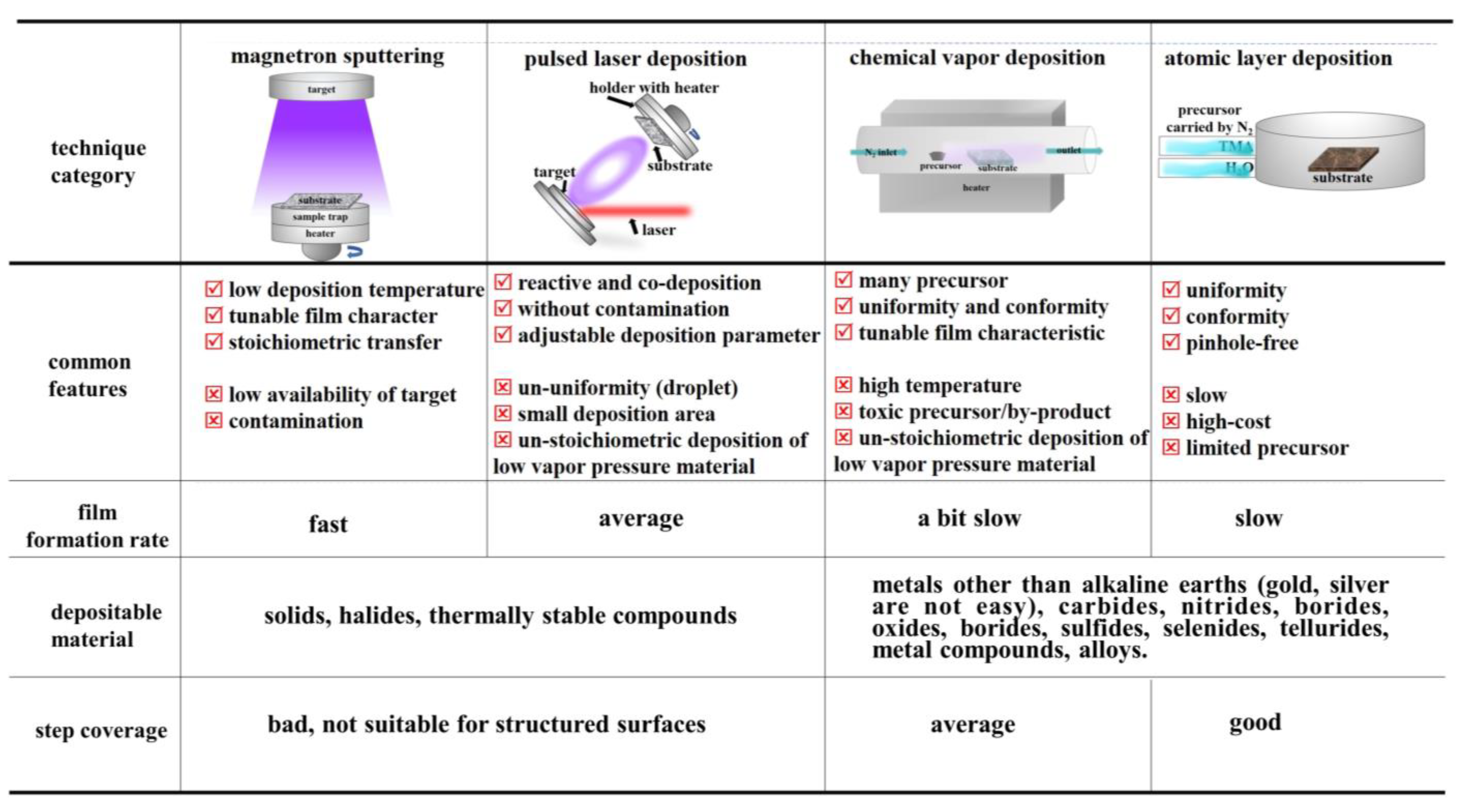
Figure 1. Schematic illustration of main characteristics of advanced deposition techniques.
Apart from the above-mentioned coating method, there also exist other approaches such as vacuum evaporation, molecular beam epitaxy(MBE), and ion plating [61], extensively employed in lithium-ion batteries. The working mechanism of vacuum evaporation involves the heating of the material to its boiling point, causing it to evaporate and form a thin film on the substrate. The deposition rate is controlled by the heating rate of the material and the pressure in the vacuum chamber; The working mechanism of MBE involves the formation of a thin film on the substrate through the deposition of neutral particles. The deposition rate is controlled by the flux of particles and the substrate temperature; The working mechanism of ion implantation involves the modification of the surface composition and structure through the implantation of ions. The implantation depth and concentration are controlled by the energy of the ions and the dose of ions implanted into the surface. In general, each of these techniques offers different advantages and disadvantages, and the choice of technique will depend on the specific requirements of the application. However, all of these techniques can be used to deposit thin films with precise control over the film thickness, composition, and microstructure, making them useful for a variety of applications, including surface modification of lithium-ion batteries.
Impressively, the small and low-cost vacuum-based coating equipment is welcomed in a laboratory for cutting-edge investigation. Certainly, coating techniques with new working principle, high coating efficiency and exactly controlling film quality is highly desired.
This entry is adapted from the peer-reviewed paper 10.3390/coatings13030505
References
- Vu, T.D.; Jin, P.; Chen, Z.; Gao, Y.; Long, Y. Physical Vapor Deposition and its application in vanadium dioxide synthesis. In Vanadium Dioxide-based Thermochromic Smart Windows; Jenny Stanford Publishing: Singapore, 2021; pp. 251–326.
- Hamon, Y.; Brousse, T.; Jousse, F.; Topart, P.; Buvat, P.; Schleich, D.M. Aluminum negative electrode in lithium ion batteries. J. Power Sources 2001, 97–98, 185–187.
- Abid, N.; Khan, M.; Shujait, S.; Chaudhary, K.; Ikram, M.; Imran, M.; Haider, J.; Khan, M.; Khan, Q.; Maqbool, M. Synthesis of nanomaterials using various top-down and bottom-up approaches, influencing factors, advantages, and disadvantages: A review. Adv. Colloid Interface Sci. 2022, 300, 102597.
- Grove, W.R. On the electro-chemical polarity of gases. Philos. Trans. R. Soc. Lond. 1852, 142, 87–101.
- Karimi, P.M. Atomic Mechanisms of Stress Formation of Group IVB-VIB Transition Metal Nitrides Deposited by DC Magnetron Sputtering. Ph.D. Thesis, RWTH Aachen University, Aachen, Germany, 2007.
- Thanit, S. Work Function of Indium Tin Oxide Studied by Photoemission Spectroscopy. Ph.D. Thesis, School of Physics Institute of Science Suranaree University of Technology, Nakhon Ratchasima, Thailand, 2016.
- Sun, Z.; Liu, L.; Yang, B.; Li, Q.; Wu, B.; Zhao, J.; Ma, L.; Liu, Y.; An, H. Preparation and ion conduction of Li1.5Al0.5Ge1.5(PO4)3 solid electrolyte films using radio frequency sputtering. Solid State Ion. 2020, 346, 115224.
- Franssila, S. Introduction to Microfabrication; John Wiley & Sons: Hoboken, NJ, USA, 2010.
- Swann, S. Magnetron sputtering. Phys. Technol. 1988, 19, 67–75.
- Banerjee, A.N.; Ghosh, C.K.; Chattopadhyay, K.K.; Minoura, H.; Sarkar, A.K.; Akiba, A.; Kamiya, A.; Endo, T. Low-temperature deposition of ZnO thin films on PET and glass substrates by DC-sputtering technique. Thin Solid Films 2006, 496, 112–116.
- Sato, H.; Minami, T.; Takata, S.; Mouri, T.; Ogawa, N. Highly conductive and transparent ZnO:Al thin films prepared on high-temperature substrates by d.c. magnetron sputtering. Thin Solid Films 1992, 220, 327–332.
- Pethe, S.A.; Takahashi, E.; Kaul, A.; Dhere, N.G. Effect of sputtering process parameters on film properties of molybdenum back contact. Sol. Energy Mater. Sol. Cells 2012, 100, 1–5.
- Cuniot-Ponsard, M.; Desvignes, J.-M.; Ea-Kim, B.; Leroy, E. Radio frequency magnetron sputtering deposition of hetero-epitaxial strontium barium niobate thin films (SrxBa1−xNb2O6). J. Appl. Phys. 2003, 93, 1718–1724.
- Stan, G.E.; Morosanu, C.O.; Marcov, D.A.; Pasuk, I.; Miculescu, F.; Reumont, G. Effect of annealing upon the structure and adhesion properties of sputtered bio-glass/titanium coatings. Appl. Surf. Sci. 2009, 255, 9132–9138.
- Raman, P.; Shchelkanov, I.A.; McLain, J.; Ruzic, D.N. High power pulsed magnetron sputtering: A method to increase deposition rate. J. Vac. Sci. Technol. A Vac. Surf. Film. 2015, 33, 031304.
- Bräuer, G.; Szyszka, B.; Vergöhl, M.; Bandorf, R. Magnetron sputtering-Milestones of 30 years. Vacuum 2010, 84, 1354–1359.
- Michaluk, C.A. Correlating discrete orientation and grain size to the sputter deposition properties of tantalum. J. Electron. Mater. 2002, 31, 2–9.
- Schou, J. Physical aspects of the pulsed laser deposition technique: The stoichiometric transfer of material from target to film. Appl. Surf. Sci. 2009, 255, 5191–5198.
- Cesaria, M.; Mazzeo, M.; Quarta, G.; Aziz, M.R.; Nobile, C.; Carallo, S.; Martino, M.; Calcagnile, L.; Caricato, A.P. Pulsed Laser Deposition of CsPbBr3 Films: Impact of the Composition of the Target and Mass Distribution in the Plasma Plume. Nanomaterials 2021, 11, 3210.
- Patel, D.; Pandey, S.; Bhattacharjee, S. Size-controlled growth of nanoparticles and clusters during pulsed laser ablation into an ambient wave induced plasma. Appl. Surf. Sci. 2018, 462, 373–377.
- Sanz, M.; Walczak, M.; Oujja, M.; Cuesta, A.; Castillejo, M. Nanosecond pulsed laser deposition of TiO2: Nanostructure and morphology of deposits and plasma diagnosis. Thin Solid Films 2009, 517, 6546–6552.
- Matsuda, Y.; Kuwata, N.; Kawamura, J. Thin-film lithium batteries with 0.3–30 μm thick LiCoO2 films fabricated by high-rate pulsed laser deposition. Solid State Ion. 2018, 320, 38–44.
- Aguesse, F.; Roddatis, V.; Roqueta, J.; García, P.; Pergolesi, D.; Santiso, J.; Kilner, J.A. Microstructure and ionic conductivity of LLTO thin films: Influence of different substrates and excess lithium in the target. Solid State Ion. 2015, 272, 1–8.
- Bharathi, K.K.; Tan, H.; Takeuchi, S.; Meshi, L.; Shen, H.; Shin, J.; Takeuchi, I.; Bendersky, L.A. Effect of oxygen pressure on structure and ionic conductivity of epitaxial Li0.33La0.55TiO3 solid electrolyte thin films produced by pulsed laser deposition. RSC Adv. 2016, 6, 61974–61983.
- Biserni, E.; Scarpellini, A.; Brescia, R.; Dellasega, D.; Li Bassi, A.; Bruno, P. Room temperature fabrication of silicon nanocrystals by pulsed laser deposition. J. Nanoparticle Res. 2014, 16, 2461.
- Xie, Z.; Duo, Y.; Lin, Z.; Fan, T.; Xing, C.; Yu, L.; Wang, R.; Qiu, M.; Zhang, Y.; Zhao, Y. The rise of 2D photothermal materials beyond graphene for clean water production. Adv. Sci. 2020, 7, 1902236.
- Oka, D.; Hirose, Y.; Fukumura, T.; Hasegawa, T. Heteroepitaxial growth of perovskite CaTaO2N thin films by nitrogen plasma-assisted pulsed laser deposition. Cryst. Growth Des. 2014, 14, 87–90.
- Soto, G. AES, EELS and XPS characterization of Ti(C, N, O) films prepared by PLD using a Ti target in N2, CH4, O2 and CO as reactive gases. Appl. Surf. Sci. 2004, 233, 115–122.
- Koralli, P.; Petropoulou, G.; Mouzakis, D.E.; Mousdis, G.; Kompitsas, M. Efficient CO sensing by a CuO:Au nanocomposite thin film deposited by PLD on a Pyrex tube. Sens. Actuators A Phys. 2021, 332, 113120.
- Bai, G.; Wang, C.; Luo, M.; Wang, J.; Luo, Q.; Luo, J.; Wang, B.; Zhao, J. High-performance tin-titanium thin-film anodes prepared by magnetron co-sputtering for lithium-ion microbatteries. J. Solid State Electrochem. 2019, 23, 2835–2841.
- Sastre, J.; Lin, T.-Y.; Filippin, A.N.; Priebe, A.; Avancini, E.; Michler, J.; Tiwari, A.N.; Romanyuk, Y.E.; Buecheler, S. Aluminum-assisted densification of cosputtered lithium garnet electrolyte films for solid-state batteries. ACS Appl. Energy Mater. 2019, 2, 8511–8524.
- Xiao, D.-L.; Tong, J.; Feng, Y.; Zhong, G.-H.; Li, W.-J.; Yang, C.-L. Improved performance of all-solid-state lithium batteries using LiPON electrolyte prepared with Li-rich sputtering target. Solid State Ion. 2018, 324, 202–206.
- Tan, G.; Bao, W.; Yuan, Y.; Liu, Z.; Shahbazian-Yassar, R.; Wu, F.; Amine, K.; Wang, J.; Lu, J. Freestanding highly defect nitrogen-enriched carbon nanofibers for lithium ion battery thin-film anodes. J. Mater. Chem. A 2017, 5, 5532–5540.
- Carlsson, J.-O.; Martin, P.M. Chapter 7—Chemical vapor deposition. In Handbook of Deposition Technologies for Films and Coatings, 3rd ed.; Martin, P.M., Ed.; William Andrew Publishing: Boston, MA, USA, 2010; pp. 314–363.
- Nigro, R.L.; Schilirò, E.; Mannino, G.; Di Franco, S.; Roccaforte, F. Comparison between thermal and plasma enhanced atomic layer deposition processes for the growth of HfO2 dielectric layers. J. Cryst. Growth 2020, 539, 125624.
- van den Bruele, F.J.; Smets, M.; Illiberi, A.; Creyghton, Y.; Buskens, P.; Roozeboom, F.; Poodt, P. Atmospheric pressure plasma enhanced spatial ALD of silver. J. Vac. Sci. Technol. A Vac. Surf. Film. 2015, 33, 01A131.
- Miikkulainen, V.; Väyrynen, K.; Kilpi, V.; Han, Z.; Vehkamäki, M.; Mizohata, K.; Räisänen, J.; Ritala, M. Photo-assisted ALD: Process development and application perspectives. ECS Trans. 2017, 80, 49.
- Coffey, B.M.; Nallan, H.C.; Engstrom, J.R.; Lam, C.H.; Ekerdt, J.G. Vacuum ultraviolet-enhanced oxidation—A route to the atomic layer etching of palladium metal. Chem. Mater. 2020, 32, 6035–6042.
- Chu, S.-Y.; Shen, M.-X.; Yeh, T.-H.; Chen, C.-H.; Lee, C.-T.; Lee, H.-Y. Investigation of Ga2O3-based deep ultraviolet photodetectors using plasma-enhanced atomic layer deposition system. Sensors 2020, 20, 6159.
- Kim, T.-H.; Lee, K.-M.; Hwang, J.-D.; Hong, W.-S. Nanocrystalline silicon films deposited with a modulated hydrogen dilution ratio by catalytic CVD at 200 °C. Curr. Appl. Phys. 2009, 9, e108–e110.
- Zhang, Y.; Zhang, L.; Zhou, C. Review of chemical vapor deposition of graphene and related applications. Acc. Chem. Res. 2013, 46, 2329–2339.
- Perera, K.; Kam, N.; Ademi, Z.; Liew, D.; Zomer, E. Bempedoic acid for high-risk patients with CVD as adjunct lipid-lowering therapy: A cost-effectiveness analysis. J. Clin. Lipidol. 2020, 14, 772–783.
- Hareesh, R.; Vetrivendan, E.; Sole, R.; Ningshen, S. Surface characterization and influence of pyrolysis temperature on microstructure, phase and oxidation kinetics of CVD pyrolytic graphite coatings. Appl. Surf. Sci. 2020, 529, 147106.
- Son, I.H.; Park, J.H.; Park, S.; Park, K.; Han, S.; Shin, J.; Doo, S.-G.; Hwang, Y.; Chang, H.; Choi, J.W. Graphene balls for lithium rechargeable batteries with fast charging and high volumetric energy densities. Nat. Commun. 2017, 8, 1561.
- Sherrell, P.C.; Palczynski, P.; Sokolikova, M.S.; Reale, F.; Pesci, F.M.; Och, M.; Mattevi, C. Large-Area CVD MoS2/WS2 heterojunctions as a photoelectrocatalyst for salt-water oxidation. ACS Appl. Energy Mater. 2019, 2, 5877–5882.
- Shawkat, M.S.; Chung, H.-S.; Dev, D.; Das, S.; Roy, T.; Jung, Y. Two-dimensional/three-dimensional Schottky junction photovoltaic devices realized by the direct CVD growth of vdw 2D PtSe2 layers on silicon. ACS Appl. Mater. Interfaces 2019, 11, 27251–27258.
- Yan, K.; Fu, L.; Peng, H.; Liu, Z. Designed CVD growth of graphene via process engineering. Acc. Chem. Res. 2013, 46, 2263–2274.
- Jones, A.C.; Hitchman, M.L. Chemical Vapour Deposition: Precursors, Processes and Applications; Royal Society of Chemistry: London, UK, 2009.
- Chen, J.; Tang, W.; Tian, B.; Liu, B.; Zhao, X.; Liu, Y.; Ren, T.; Liu, W.; Geng, D.; Jeong, H.Y. Chemical vapor deposition of high-quality large-sized MoS2 crystals on silicon dioxide substrates. Adv. Sci. 2016, 3, 1500033.
- Chen, Y.; Zhang, X.; Liu, E.; He, C.; Han, Y.; Li, Q.; Nash, P.; Zhao, N. Fabrication of three-dimensional graphene/Cu composite by in-situ CVD and its strengthening mechanism. J. Alloy. Compd. 2016, 688, 69–76.
- Vesel, A.; Zaplotnik, R.; Primc, G.; Paul, D.; Mozetič, M. Comparison of plasma deposition of carbon nanomaterials using various polymer materials as a carbon atom source. Nanomaterials 2022, 12, 246.
- Gleason, K.K. Nanoscale control by chemically vapour-deposited polymers. Nat. Rev. Phys. 2020, 2, 347–364.
- Hu, Y.; Lu, J.; Feng, H. Surface modification and functionalization of powder materials by atomic layer deposition: A review. RSC Adv. 2021, 11, 11918–11942.
- Cai, J.; Han, X.; Wang, X.; Meng, X. Atomic layer deposition of two-dimensional layered materials: Processes, growth mechanisms, and characteristics. Matter 2020, 2, 587–630.
- Shi, H.; Zhang, H.; Li, X.; Du, Y.; Hou, G.; Xiang, M.; Lv, P.; Zhu, Q. In situ fabrication of dual coating structured SiO/1D-C/a-C composite as high-performance lithium ion battery anode by fluidized bed chemical vapor deposition. Carbon 2020, 168, 113–124.
- Tiznado, H.; Domínguez, D.; Muñoz-Muñoz, F.; Romo-Herrera, J.; Machorro, R.; Contreras, O.E.; Soto, G. Pulsed-bed atomic layer deposition setup for powder coating. Powder Technol. 2014, 267, 201–207.
- Kotlarski, G.; Valkov, S.; Andreeva, A.; Mateev, V.; Marinova, I.; Petrov, P. Electrical contact resistance of tungsten coatings deposited on Cu and Al conductors. J. Phys. Conf. Ser. 2021, 1859, 012063.
- Dushik, V.V.; Redkina, G.V.; Rozhanskii, N.V.; Rybkina, T.V.; Shaporenkov, A.A.; Maschenko, V.E. Corrosion and electrochemical behavior of β-W CVD coatings in NaCl solution. Prot. Met. Phys. Chem. Surf. 2020, 56, 1321–1324.
- Mahan, J.E. Physical Vapor Deposition of Thin Films; Wiley-VCH: Hoboken, NJ, USA, 2000; p. 336.
- Olayinka Oluwatosin, A.; Esther Titilayo, A.; Oluseyi Philip, O.; Stephen, A.; Albert Uchenna, U. Overview of thin film deposition techniques. AIMS Mater. Sci. 2019, 6, 174–199.
- Seshan, K. Handbook of Thin Film Deposition Techniques Principles, Methods, Equipment and Applications, 2nd ed.; CRC Press: Boca Raton, FL, USA, 2002.
This entry is offline, you can click here to edit this entry!