The conventional boost DC/DC converter is used to step up the input voltage to a desired higher level within the practical limit required by the load with very few components. Stepping up the voltage is achieved by storing the energy in the inductor and releasing it to the output at a higher voltage. The boost converter is very popular for capacitive load applications such as photo-flashers and battery chargers. It is also used in automotive applications, power amplifiers, adaptive control applications, battery power systems, consumer electronics, DC motor drives and power factor correction circuits.
- high voltage gain
- DC/DC converter
- step-up techniques
1. High Step-Up Techniques
2. Multistage/Multilevel Structures
2.1. Cascaded Topology
2.1.1. Symmetric and Non-Symmetric Converters

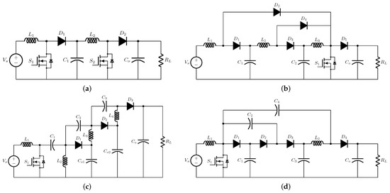
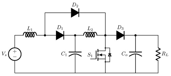
2.1.2. Quadratic Boost Converters (QBC)
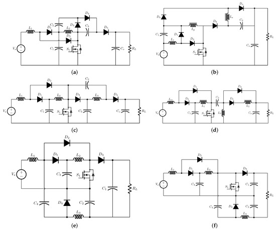
2.2. Interleaved Converters
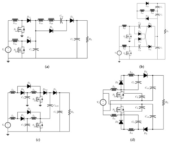
2.3. Multilevel Converters
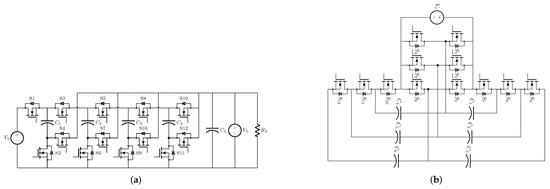
3. Switched Capacitor (SC)
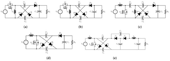
4. Voltage Multiplier
5. Voltage Lift (VL)
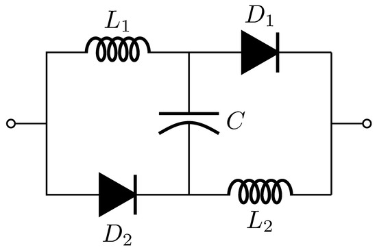
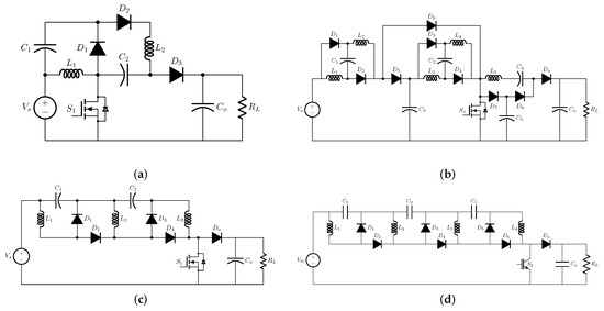
6. Switched Inductor (SL)
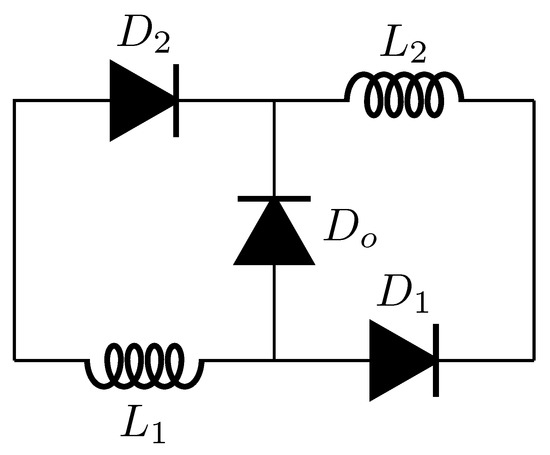
7. Magnetic Coupling
7.1. Transformer
7.2. Coupled Inductor
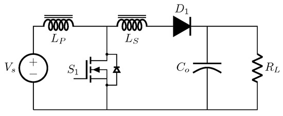
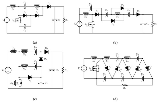
7.3. Multi-Track Structure
This entry is adapted from the peer-reviewed paper 10.3390/electronics12030718
References
- Morales-Saldana, J.; Gutierrez, E.; Leyva-Ramos, J. Modeling of switch-mode dc-dc cascade converters. IEEE Trans. Aerosp. Electron. Syst. 2002, 38, 295–299.
- Wu, T.F.; Yu, T.H. Unified approach to developing single-stage power converters. IEEE Trans. Aerosp. Electron. Syst. 1998, 34, 211–223.
- Haroun, R.; Cid-Pastor, A.; Aroudi, A.E.; Martínez-Salamero, L. Synthesis of Canonical Elements for Power Processing in DC Distribution Systems Using Cascaded Converters and Sliding-Mode Control. IEEE Trans. Power Electron. 2014, 29, 1366–1381.
- Leyva-Ramos, J.; Ortiz-Lopez, M.; Diaz-Saldierna, L.; Morales-Saldana, J. Switching regulator using a quadratic boost converter for wide DC conversion ratios. IET Power Electron. 2009, 2, 605–613.
- López-Santos, O.; Martínez-Salamero, L.; García, G.; Valderrama-Blavi, H.; Mercuri, D.O. Efficiency analysis of a sliding-mode controlled quadratic boost converter. IET Power Electron. 2013, 6, 364–373.
- Choudhury, T.R.; Nayak, B. Comparison and analysis of cascaded and Quadratic Boost Converter. In Proceedings of the 2015 IEEE Power, Communication and Information Technology Conference (PCITC), Bhubaneswar, India, 15–17 October 2015; pp. 78–83.
- Boujelben, N.; Masmoudi, F.; Djemel, M.; Derbel, N. Design and comparison of quadratic boost and double cascade boost converters with boost converter. In Proceedings of the 2017 14th International Multi-Conference on Systems, Signals and Devices (SSD), Marrakech, Morocco, 28–31 March 2017; pp. 245–252.
- Chen, Z.; Yong, W.; Gao, W. PI and Sliding Mode Control of a Multi-Input-Multi-Output Boost-Boost Converter. WSEAS Trans. Power Syst. 2014, 9, 87–102.
- Amir, A.; Amir, A.; Che, H.S.; Elkhateb, A.; Abd Rahim, N. Comparative analysis of high voltage gain DC-DC converter topologies for photovoltaic systems. Renew. Energy 2019, 136, 1147–1163.
- Feng, X.; Liu, J.; Lee, F. Impedance specifications for stable DC distributed power systems. IEEE Trans. Power Electron. 2002, 17, 157–162.
- Leyva Ramos, J.; Ortiz-Lopez, M.G.; Morales-Saldana, J.A. Control of a cascade boost converter with a single active switch. In Proceedings of the 2008 IEEE Power Electronics Specialists Conference, Rhodes, Greece, 15–19 June 2008; pp. 2383–2388.
- Ortiz-Lopez, M.G.; Leyva-Ramos, J.; Diaz-Saldierna, L.H.; Carbajal-Gutierrez, E.E. Multiloop Controller for N-Stage Cascade Boost Converter. In Proceedings of the 2007 IEEE International Conference on Control Applications, Singapore, 1–3 October 2007; pp. 587–592.
- Andrade, A.M.S.S.; Hey, H.L.; Schuch, L.; da Silva Martins, M.L. Comparative Evaluation of Single Switch High-Voltage Step-Up Topologies Based on Boost and Zeta PWM Cells. IEEE Trans. Ind. Electron. 2018, 65, 2322–2334.
- Banaei, M.R.; Sani, S.G. Analysis and Implementation of a New SEPIC-Based Single-Switch Buck–Boost DC–DC Converter With Continuous Input Current. IEEE Trans. Power Electron. 2018, 33, 10317–10325.
- Sabzali, A.J.; Ismail, E.H.; Behbehani, H.M. High voltage step-up integrated double Boost–Sepic DC–DC converter for fuel-cell and photovoltaic applications. Renew. Energy 2015, 82, 44–53.
- Wijeratne, D.S.; Moschopoulos, G. Quadratic Power Conversion for Power Electronics: Principles and Circuits. IEEE Trans. Circuits Syst. Regul. Pap. 2012, 59, 426–438.
- Zhang, S.; Xu, J.; Yang, P. A single-switch high gain quadratic boost converter based on voltage-lift-technique. In Proceedings of the 2012 10th International Power and Energy Conference (IPEC), Ho Chi Minh City, Vietnam, 12–14 December 2012; pp. 71–75.
- Morales-Saldana, J.A.; Loera-Palomo, R.; Palacios-Hernández, E.; Gonzalez-Martinez, J.L. Modelling and control of a DC-DC quadratic boost converter with R 2 P 2. IET Power Electron. 2014, 7, 11–22.
- Ye, Y.m.; Cheng, K.W.E. Quadratic boost converter with low buffer capacitor stress. IET Power Electron. 2014, 7, 1162–1170.
- Kadri, R.; Gaubert, J.P.; Champenois, G.; Mostefaï, M. Performance analysis of transformless single switch quadratic boost converter for grid connected photovoltaic systems. In Proceedings of the The XIX International Conference on Electrical Machines - ICEM 2010, Rome, Italy, 6–8 September 2010; pp. 1–7.
- Alkhaldi, A.; Akbar, F.; Elkhateb, A.; Laverty, D. N-Stage Quadratic Boost Converter Based on Voltage Lift Technique and Voltage Multiplier. In Proceedings of the The 11th International Conference on Power Electronics, Machines and Drives (PEMD 2022), Newcastle, UK, 21–23 June 2022.
- Veerachary, M.; Kumar, N. Analysis and Design of Quadratic Following Boost Converter. IEEE Trans. Ind. Appl. 2020, 56, 6657–6673.
- Veerachary, M.; Kumar, N. Modified Quadratic Following Boost Converter - Robustness Considerations. In Proceedings of the 2020 IEEE International Conference on Computing, Power and Communication Technologies (GUCON), Greater Noida, India, 2–4 October 2020; pp. 745–750.
- Lee, S.W.; Do, H.L. Quadratic Boost DC–DC Converter With High Voltage Gain and Reduced Voltage Stresses. IEEE Trans. Power Electron. 2019, 34, 2397–2404.
- Jahangiri, H.; Mohammadpour, S.; Ajami, A. A high step-up DC-DC boost converter with coupled inductor based on quadratic converters. In Proceedings of the 2018 9th Annual Power Electronics, Drives Systems and Technologies Conference (PEDSTC), Tehran, Iran, 13–15 February 2018; pp. 20–25.
- Maheshwari, M.; Arounassalame, M. A Novel Integrated High Gain DC-DC Converter. In Proceedings of the 2019 IEEE International Conference on Electrical, Computer and Communication Technologies (ICECCT), Coimbatore, India, 20–22 February 2019; pp. 1–6.
- Axelrod, B.; Berkovich, Y.; Beck, Y. New Quadratic Sepic Converter with a Switched-Coupled Inductor. In Proceedings of the 2018 20th European Conference on Power Electronics and Applications (EPE’18 ECCE Europe), Riga, Latvia, 17–21 September 2018; pp. P.1–P.9.
- Andrade, A.M.S.S.; Martins, M.L.d.S. Quadratic-Boost With Stacked Zeta Converter for High Voltage Gain Applications. IEEE J. Emerg. Sel. Top. Power Electron. 2017, 5, 1787–1796.
- Pires, V.F.; Cordeiro, A.; Foito, D.; Silva, J.F. High Step-Up DC–DC Converter for Fuel Cell Vehicles Based on Merged Quadratic Boost–Ćuk. IEEE Trans. Veh. Technol. 2019, 68, 7521–7530.
- Li, G.; Jin, X.; Chen, X.; Mu, X. A novel quadratic boost converter with low inductor currents. CPSS Trans. Power Electron. Appl. 2020, 5, 1–10.
- Hu, X.; Gong, C. A High Voltage Gain DC–DC Converter Integrating Coupled-Inductor and Diode–Capacitor Techniques. IEEE Trans. Power Electron. 2014, 29, 789–800.
- Zhang, N.; Sutanto, D.; Muttaqi, K.M.; Zhang, B.; Qiu, D. High-voltage-gain quadratic boost converter with voltage multiplier. IET Power Electron. 2015, 8, 2511–2519.
- Ghafour, Z.A.; Ajel, A.R.; Yasin, N.M. A New High Gain Quadratic DC-DC Boost Converter for Photovoltaic Applications. In Proceedings of the 2022 10th International Conference on Smart Grid (icSmartGrid), Istanbul, Turkey, 27–29 June 2022; pp. 137–144.
- Alizadeh, D.; Babaei, E.; Sabahi, M. High Step-Up Quadratic Impedance Source DC-DC Converter Based on Coupled Inductor. IEEE J. Emerg. Sel. Top. Power Electron. 2022.
- Gupta, A.; Korada, N.; Ayyanar, R. Quadratic-Extended-Duty-Ratio Boost Converters for Ultra High Gain Application with Low Input Current Ripple and Low Device Stress. IEEE Trans. Ind. Appl. 2022, 1–11.
- Abbasi, V.; Rostami, S.; Hemmati, S.; Ahmadian, S. Ultrahigh Step-Up Quadratic Boost Converter Using Coupled Inductors With Low Voltage Stress on the Switches. IEEE J. Emerg. Sel. Top. Power Electron. 2022, 10, 7733–7743.
- Li, W.; Zhao, Y.; Deng, Y.; He, X. Interleaved Converter With Voltage Multiplier Cell for High Step-Up and High-Efficiency Conversion. IEEE Trans. Power Electron. 2010, 25, 2397–2408.
- Tseng, K.C.; Huang, C.C. High Step-Up High-Efficiency Interleaved Converter With Voltage Multiplier Module for Renewable Energy System. IEEE Trans. Ind. Electron. 2014, 61, 1311–1319.
- Li, W.; Xiang, X.; Li, C.; Li, W.; He, X. Interleaved High Step-Up ZVT Converter with Built-In Transformer Voltage Doubler Cell for Distributed PV Generation System. IEEE Trans. Power Electron. 2013, 28, 300–313.
- Samuel, V.J.; Keerthi, G.; Prabhakar, M. High Gain Interleaved Quadratic Boost DCDC Converter. In Proceedings of the 2019 2nd International Conference on Power and Embedded Drive Control (ICPEDC), Chennai, India, 21–23 August 2019; pp. 390–395.
- Tseng, S.Y.; Hsu, C.Y. Interleaved step-up converter with a single-capacitor snubber for PV energy conversion applications. Int. J. Electr. Power Energy Syst. 2013, 53, 909–922.
- Li, W.; Wu, J.; Wang, D.; Deng, Y.; He, X. A Family of Interleaved DC/DC Convert Deduced from a Basic Cell with Winding-Coupled Inductors for High Step-Up/Step-Down Conversions. In Proceedings of the 2007 IEEE Power Electronics Specialists Conference, Orlando, FL, USA, 17–21 June 2007; pp. 2335–2340.
- Li, W.; He, X. An Interleaved Winding-Coupled Boost Converter With Passive Lossless Clamp Circuits. IEEE Trans. Power Electron. 2007, 22, 1499–1507.
- Mittle, A.; Singh, R.K.; J, S.C. A New Interleaved High Step-up DC-DC Converter. In Proceedings of the 2019 IEEE Students Conference on Engineering and Systems (SCES), Allahabad, India, 29–31 May 2019; pp. 1–5.
- Sedaghati, F.; Eskandarpour Azizkandi, M.; Majareh, S.H.L.; Shayeghi, H. A High-Efficiency Non-Isolated High-Gain Interleaved DC-DC Converter with Reduced Voltage Stress on Devices. In Proceedings of the 2019 10th International Power Electronics, Drive Systems and Technologies Conference (PEDSTC), Shiraz, Iran, 12–14 February 2019; pp. 729–734.
- Alghaythi, M.L.; O’Connell, R.M.; Islam, N.E.; Khan, M.M.S.; Guerrero, J.M. A High Step-Up Interleaved DC-DC Converter With Voltage Multiplier and Coupled Inductors for Renewable Energy Systems. IEEE Access 2020, 8, 123165–123174.
- Zhang, F.; Peng, F.; Qian, Z. Study of the multilevel converters in DC-DC applications. In Proceedings of the 2004 IEEE 35th Annual Power Electronics Specialists Conference (IEEE Cat. No.04CH37551), Aachen, Germany, 20–25 June 2004; Volume 2, pp. 1702–1706.
- Forouzesh, M.; Siwakoti, Y.P.; Gorji, S.A.; Blaabjerg, F.; Lehman, B. A survey on voltage boosting techniques for step-up DC-DC converters. In Proceedings of the 2016 IEEE Energy Conversion Congress and Exposition (ECCE), Milwaukee, WI, USA, 18–22 September 2016; pp. 1–8.
- Khan, F.H.; Tolbert, L.M. A Multilevel Modular Capacitor-Clamped DC–DC Converter. IEEE Trans. Ind. Appl. 2007, 43, 1628–1638.
- Cao, D.; Peng, F.Z. Zero-Current-Switching Multilevel Modular Switched-Capacitor DC–DC Converter. IEEE Trans. Ind. Appl. 2010, 46, 2536–2544.
- Khan, F.H.; Tolbert, L.M. Multiple-Load–Source Integration in a Multilevel Modular Capacitor-Clamped DC–DC Converter Featuring Fault Tolerant Capability. IEEE Trans. Power Electron. 2009, 24, 14–24.
- Qian, W.; Cao, D.; Cintron-Rivera, J.G.; Gebben, M.; Wey, D.; Peng, F.Z. A Switched-Capacitor DC–DC Converter With High Voltage Gain and Reduced Component Rating and Count. IEEE Trans. Ind. Appl. 2012, 48, 1397–1406.
- Walker, G.; Sernia, P. Cascaded DC-DC converter connection of photovoltaic modules. IEEE Trans. Power Electron. 2004, 19, 1130–1139.
- Echeverría, J.; Kouro, S.; Pérez, M.; Abu-rub, H. Multi-modular cascaded DC-DC converter for HVDC grid connection of large-scale photovoltaic power systems. In Proceedings of the IECON 2013 - 39th Annual Conference of the IEEE Industrial Electronics Society, Vienna, Austria, 10–13 November 2013; pp. 6999–7005.
- Rivera, S.; Kouro, S.; Wu, B.; Leon, J.I.; Rodríguez, J.; Franquelo, L.G. Cascaded H-bridge multilevel converter multistring topology for large scale photovoltaic systems. In Proceedings of the 2011 IEEE International Symposium on Industrial Electronics, Gdansk, Poland, 27–30 June 2011; pp. 1837–1844.
- Kutkut, N.; Divan, D. Dynamic equalization techniques for series battery stacks. In Proceedings of the Proceedings of Intelec’96 - International Telecommunications Energy Conference, Boston, MA, USA, 6–10 October 1996; pp. 514–521.
- Cheong, S.; Chung, S.; Ioinovici, A. Development of power electronics converters based on switched-capacitor circuits. In Proceedings of the 1992 IEEE International Symposium on Circuits and Systems, San Diego, CA, USA, 10–13 May 1992; Volume 4, pp. 1907–1910.
- Ueno, F.; Inoue, T.; Umeno, T.; Oota, I. Analysis and application of switched-capacitor transformers by formulation. Electron. Commun. Jpn. Part Ii: Electron. 1990, 73, 91–103.
- Cheong, S.; Chung, H.; Ioinovici, A. Inductorless DC-to-DC converter with high power density. IEEE Trans. Ind. Electron. 1994, 41, 208–215.
- Mak, O.C.; Wong, Y.C.; Ioinovici, A. Step-up DC power supply based on a switched-capacitor circuit. IEEE Trans. Ind. Electron. 1995, 42, 90–97.
- Seeman, M.D. A Design Methodology for Switched-Capacitor DC-DC Converters; University of California: Berkeley, CA, USA, 2009.
- Ioinovici, A. Switched-capacitor power electronics circuits. IEEE Circuits Syst. Mag. 2001, 1, 37–42.
- Ismail, E.H.; Al-Saffar, M.A.; Sabzali, A.J.; Fardoun, A.A. A Family of Single-Switch PWM Converters With High Step-Up Conversion Ratio. IEEE Trans. Circuits Syst. Regul. Pap. 2008, 55, 1159–1171.
- Hassan, W.; Lu, D.D.C.; Xiao, W. Single-Switch High Step-Up DC–DC Converter with Low and Steady Switch Voltage Stress. IEEE Trans. Ind. Electron. 2019, 66, 9326–9338.
- Umeno, T.; Takahashi, K.; Ueno, F.; Inoue, T.; Oota, I. A new approach to low ripple-noise switching converters on the basis of switched-capacitor converters. In Proceedings of the 1991., IEEE International Sympoisum on Circuits and Systems, Singapore, 11–14 June 1991; pp. 1077–1080.
- Li, S.; Li, Z.; Shang, W.; Zheng, S.; Jia, P. A Family of Hybrid Step-up DC-DC Converters based on Switched-capacitor Converters. In Proceedings of the 2020 IEEE 9th International Power Electronics and Motion Control Conference (IPEMC2020-ECCE Asia), Nanjing, China, 29 November–2 December 2020; pp. 497–502.
- Lei, H.; Hao, R.; You, X.; Li, F. Nonisolated High Step-Up Soft-Switching DC–DC Converter With Interleaving and Dickson Switched-Capacitor Techniques. IEEE J. Emerg. Sel. Top. Power Electron. 2020, 8, 2007–2021.
- Law, K.; Cheng, K.; Yeung, Y. Design and analysis of switched-capacitor-based step-up resonant converters. IEEE Trans. Circuits Syst. Regul. Pap. 2005, 52, 943–948.
- Schaef, C.; Stauth, J.T. A Highly Integrated Series–Parallel Switched-Capacitor Converter with 12 V Input and Quasi-Resonant Voltage-Mode Regulation. IEEE J. Emerg. Sel. Top. Power Electron. 2018, 6, 456–464.
- Prudente, M.; Pfitscher, L.L.; Emmendoerfer, G.; Romaneli, E.F.; Gules, R. Voltage Multiplier Cells Applied to Non-Isolated DC–DC Converters. IEEE Trans. Power Electron. 2008, 23, 871–887.
- Axelrod, B.; Berkovich, Y.; Ioinovici, A. Switched-Capacitor/Switched-Inductor Structures for Getting Transformerless Hybrid DC–DC PWM Converters. IEEE Trans. Circuits Syst. Regul. Pap. 2008, 55, 687–696.
- Elmakawi, A.M.; Bayındır, K.Ç. Novel Single Switch High Gain Non-isolated DC-DC Converter for Building Integrated Photovoltaic Systems. In Proceedings of the 2019 1st Global Power, Energy and Communication Conference (GPECOM), Nevsehir, Turkey, 12–15 June 2019; pp. 265–269.
- Moradpour, R.; Ardi, H.; Tavakoli, A. Design and Implementation of a New SEPIC-Based High Step-Up DC/DC Converter for Renewable Energy Applications. IEEE Trans. Ind. Electron. 2018, 65, 1290–1297.
- Hasanpour, S.; Baghramian, A.; Mojallali, H. A Modified SEPIC-Based High Step-Up DC–DC Converter with Quasi-Resonant Operation for Renewable Energy Applications. IEEE Trans. Ind. Electron. 2019, 66, 3539–3549.
- Zhao, Y.; Xiang, X.; Li, C.; Gu, Y.; Li, W.; He, X. Single-Phase High Step-up Converter With Improved Multiplier Cell Suitable for Half-Bridge-Based PV Inverter System. IEEE Trans. Power Electron. 2014, 29, 2807–2816.
- Lee, W.J.; Kim, C.E.; Moon, G.W.; Han, S.K. A New Phase-Shifted Full-Bridge Converter With Voltage-Doubler-Type Rectifier for High-Efficiency PDP Sustaining Power Module. IEEE Trans. Ind. Electron. 2008, 55, 2450–2458.
- Hu, X.; Gong, C. A High Gain Input-Parallel Output-Series DC/DC Converter With Dual Coupled Inductors. IEEE Trans. Power Electron. 2015, 30, 1306–1317.
- Lee, S.; Kim, P.; Choi, S. High Step-Up Soft-Switched Converters Using Voltage Multiplier Cells. IEEE Trans. Power Electron. 2013, 28, 3379–3387.
- Park, K.B.; Moon, G.W.; Youn, M.J. High Step-up Boost Converter Integrated With a Transformer-Assisted Auxiliary Circuit Employing Quasi-Resonant Operation. IEEE Trans. Power Electron. 2012, 27, 1974–1984.
- Nymand, M.; Andersen, M.A.E. High-Efficiency Isolated Boost DC–DC Converter for High-Power Low-Voltage Fuel-Cell Applications. IEEE Trans. Ind. Electron. 2010, 57, 505–514.
- Liang, T.J.; Lee, J.H.; Chen, S.M.; Chen, J.F.; Yang, L.S. Novel Isolated High-Step-Up DC–DC Converter with Voltage Lift. IEEE Trans. Ind. Electron. 2013, 60, 1483–1491.
- Luo, F.L. Luo-converters, voltage lift technique. In Proceedings of the PESC 98 Record. 29th Annual IEEE Power Electronics Specialists Conference (Cat. No.98CH36196), Fukuoka, Japan, 22 May 1998; Volume 2, pp. 1783–1789.
- Totonchi, N.; Gholizadeh, H.; Mahdizadeh, S.; Afjei, E. A High Step up DC-DC Converter Based on the Cascade Boost, Voltage Multiplier Cell and Self Lift Luo Converter. In Proceedings of the 2020 10th Smart Grid Conference (SGC), Kashan, Iran, 16–17 December 2020; pp. 1–5.
- Mohammadzadeh Shahir, F.; Babaei, E.; Farsadi, M. Voltage-Lift Technique Based Nonisolated Boost DC–DC Converter: Analysis and Design. IEEE Trans. Power Electron. 2018, 33, 5917–5926.
- Shahir, F.M.; Babaei, E.; Farsadi, M. Extended Topology for a Boost DC–DC Converter. IEEE Trans. Power Electron. 2019, 34, 2375–2384.
- Luo, F.L.; Ye, H. Advanced dc/dc Converters; CRC Press: Boca Raton, FL, USA, 2016.
- Luo, F.L. Six self-lift DC-DC converters, voltage lift technique. IEEE Trans. Ind. Electron. 2001, 48, 1268–1272.
- Zhu, M.; Luo, F. Series SEPIC implementing voltage-lift technique for DC–DC power conversion. IET Power Electron. 2008, 1, 109–121.
- Laha, A. A High Voltage Gain Quadratic Boost Converter using a Voltage Doubler and Voltage-Lift Technique. In Proceedings of the 2020 IEEE International Conference on Power Electronics, Smart Grid and Renewable Energy (PESGRE2020), Cochin, India, 2–4 January 2020; pp. 1–6.
- Chakraborty, S.; Kumar, A. A High Step-Up Transformerless DC-DC Quadratic Boost Converter using Voltage-Lift Switched Inductor and Voltage Multiplier. In Proceedings of the 2022 IEEE IAS Global Conference on Emerging Technologies (GlobConET), Arad, Romania, 20–22 May 2022; pp. 170–175.
- Li, Y.; Sathiakumar, S. Improved Quadratic Boost Converter Based on the Voltage Lift Technique. In Proceedings of the 2017 Asia Modelling Symposium (AMS), Kota Kinabalu, Malaysia, 4–6 December 2017; pp. 139–144.
- Radhika, S.; Margaret, V. A Comparative Assessment of Cascaded Double Voltage Lift Boost Converter. In Proceedings of the 2020 Fifth International Conference on Research in Computational Intelligence and Communication Networks (ICRCICN), Bangalore, India, 26–27 November 2020; pp. 177–180.
- Ye, Y.; Cheng, K.W.E. A Family of Single-Stage Switched-Capacitor–Inductor PWM Converters. IEEE Trans. Power Electron. 2013, 28, 5196–5205.
- Jiao, Y.; Luo, F.; Zhu, M. Voltage-lift-type switched-inductor cells for enhancing DC–DC boost ability: Principles and integrations in Luo converter. IET Power Electron. 2011, 4, 131–142.
- Almalaq, Y.; Alateeq, A.; Matin, M. A Non-Isolated High Gain Switched-Inductor Switched-Capacitor Step-Up Converter for Renewable Energy Applications. In Proceedings of the 2018 IEEE International Conference on Electro/Information Technology (EIT), Rochester, MI, USA, 3–5 May 2018; pp. 0134–0137.
- Choudhury, T.R.; Nayak, B.; Santra, S.B. A Novel Switch Current Stress Reduction Technique for Single Switch Boost-Flyback Integrated High Step Up DC–DC Converter. IEEE Trans. Ind. Electron. 2019, 66, 6876–6886.
- Eskandari, R.; Babaei, E.; Sabahi, M.; Ojaghkandi, S.R. Interleaved high step-up zero-voltage zero-current switching boost DC–DC converter. IET Power Electron. 2020, 13, 96–103.
- Song, W.; Lehman, B. Dual-bridge DC-DC converter: A new topology characterized with no deadtime operation. IEEE Trans. Power Electron. 2004, 19, 94–103.
- Song, W.; Lehman, B. Current-Fed Dual-Bridge DC–DC Converter. IEEE Trans. Power Electron. 2007, 22, 461–469.
- Du, Y.; Lukic, S.; Jacobson, B.; Huang, A. Review of high power isolated bi-directional DC-DC converters for PHEV/EV DC charging infrastructure. In Proceedings of the 2011 IEEE Energy Conversion Congress and Exposition, Phoenix, AZ, USA, 17–22 September 2011; pp. 553–560.
- Forouzesh, M.; Baghramian, A. Galvanically isolated high gain Y-source DC–DC converters for dispersed power generation. IET Power Electron. 2016, 9, 1192–1203.
- Husev, O.; Liivik, L.; Blaabjerg, F.; Chub, A.; Vinnikov, D.; Roasto, I. Galvanically Isolated Quasi-Z-Source DC–DC Converter With a Novel ZVS and ZCS Technique. IEEE Trans. Ind. Electron. 2015, 62, 7547–7556.
- Chub, A.; Vinnikov, D.; Blaabjerg, F.; Peng, F.Z. A Review of Galvanically Isolated Impedance-Source DC–DC Converters. IEEE Trans. Power Electron. 2016, 31, 2808–2828.
- Alhurayyis, I.; Elkhateb, A.; Morrow, J. Isolated and Nonisolated DC-to-DC Converters for Medium-Voltage DC Networks: A Review. IEEE J. Emerg. Sel. Top. Power Electron. 2021, 9, 7486–7500.
- Zhao, Q.; Lee, F. High-efficiency, high step-up DC-DC converters. IEEE Trans. Power Electron. 2003, 18, 65–73.
- Wai, R.J.; Duan, R.Y. High step-up converter with coupled-inductor. IEEE Trans. Power Electron. 2005, 20, 1025–1035.
- Hsieh, Y.P.; Chen, J.F.; Liang, T.J.; Yang, L.S. Novel High Step-Up DC–DC Converter for Distributed Generation System. IEEE Trans. Ind. Electron. 2013, 60, 1473–1482.
- Siwakoti, Y.P.; Blaabjerg, F.; Loh, P.C. Ultra-step-up DC-DC converter with integrated autotransformer and coupled inductor. In Proceedings of the 2016 IEEE Applied Power Electronics Conference and Exposition (APEC), Long Beach, CA, USA, 20–24 March 2016; pp. 1872–1877.
- Forouzesh, M.; Yari, K.; Baghramian, A.; Hasanpour, S. Single-switch high step-up converter based on coupled inductor and switched capacitor techniques with quasi-resonant operation. IET Power Electron. 2017, 10, 240–250.
- Hasanpour, S.; Siwakoti, Y.P.; Blaabjerg, F. A New High Efficiency High Step-Up DC/DC Converter for Renewable Energy Applications. IEEE Trans. Ind. Electron. 2023, 70, 1489–1500.
- Talebi, P.; Packnezhad, M.; Farzanehfard, H. Fully Soft Switched Ultra-High Step-Up Converter With Very Low Switch Voltage Stress. IEEE Trans. Power Electron. 2022, 38, 3523–3530.
- Taheri, S.M.; Baghramian, A.; Pourseyedi, S.A. A Novel High Step-Up SEPIC-Based Non-Isolated Three-Port DC-DC Converter Proper for Renewable Energy Applications. IEEE Trans. Ind. Electron. 2022.
- Habibi, S.; Rahimi, R.; Ferdowsi, M.; Shamsi, P. Coupled Inductor Based Single-Switch Quadratic High Step-Up DC-DC Converters with Reduced Voltage Stress on Switch. IEEE J. Emerg. Sel. Top. Ind. Electron. 2022, 1–12.
- Schmitz, L.; Martins, D.C.; Coelho, R.F. Three-Terminal Gain Cells Based on Coupled Inductor and Voltage Multiplers for High Step-Up Conversion. IEEE Trans. Circuits Syst. II Express Briefs 2022.
- Ardi, H.; Ajami, A.; Sabahi, M. A Novel High Step-Up DC–DC Converter With Continuous Input Current Integrating Coupled Inductor for Renewable Energy Applications. IEEE Trans. Ind. Electron. 2018, 65, 1306–1315.
- Das, M.; Pal, M.; Agarwal, V. Novel High Gain, High Efficiency DC–DC Converter Suitable for Solar PV Module Integration with Three-Phase Grid Tied Inverters. IEEE J. Photovoltaics 2019, 9, 528–537.
- Minami, M.; Tomoeda, K. An Analysis of Operation in Single-Switch High Step-up DC-DC Converter with Three-winding Coupled Inductor. In Proceedings of the 2019 IEEE Applied Power Electronics Conference and Exposition (APEC), Anaheim, CA, USA, 17–21 March 2019; pp. 2135–2137.
- Siwakoti, Y.P.; Peng, F.Z.; Blaabjerg, F.; Loh, P.C.; Town, G.E. Impedance-Source Networks for Electric Power Conversion Part I: A Topological Review. IEEE Trans. Power Electron. 2015, 30, 699–716.
- Siwakoti, Y.P.; Peng, F.Z.; Blaabjerg, F.; Loh, P.C.; Town, G.E.; Yang, S. Impedance-Source Networks for Electric Power Conversion Part II: Review of Control and Modulation Techniques. IEEE Trans. Power Electron. 2015, 30, 1887–1906.
- Siwakoti, Y.P.; Loh, P.C.; Blaabjerg, F.; Andreasen, S.J.; Town, G.E. Y-Source Boost DC/DC Converter for Distributed Generation. IEEE Trans. Ind. Electron. 2015, 62, 1059–1069.
- Siwakoti, Y.P.; Blaabjerg, F.; Loh, P.C. Quasi-Y-Source Boost DC–DC Converter. IEEE Trans. Power Electron. 2015, 30, 6514–6519.
- Siwakoti, Y.P.; Blaabjerg, F.; Chiang Loh, P. High Step-Up Trans-Inverse (Tx—1) DC–DC Converter for the Distributed Generation System. IEEE Trans. Ind. Electron. 2016, 63, 4278–4291.
- Lai, J.S.; Peng, F.Z. Multilevel converters-a new breed of power converters. IEEE Trans. Ind. Appl. 1996, 32, 509–517.
- Meynard, T.; Foch, H. Multi-level conversion: High voltage choppers and voltage-source inverters. In Proceedings of the PESC ’92 Record. 23rd Annual IEEE Power Electronics Specialists Conference, Toledo, Spain, 29 June–3 July 1992; pp. 397–403.
- Sanders, S.R.; Alon, E.; Le, H.P.; Seeman, M.D.; John, M.; Ng, V.W. The Road to Fully Integrated DC–DC Conversion via the Switched-Capacitor Approach. IEEE Trans. Power Electron. 2013, 28, 4146–4155.
- Hamma, F.; Meynard, T.; Tourkhani, F.; Viarouge, P. Characteristics and design of multilevel choppers. Proceedings of PESC ’95 - Power Electronics Specialist Conference, Atlanta, GA, USA, 18–22 June 1995; Volume 2, pp. 1208–12142.
- Sun, J.; Xu, M.; Ying, Y.; Lee, F.C. High power density, high efficiency system two-stage power architecture for laptop computers. In Proceedings of the 2006 37th IEEE Power Electronics Specialists Conference, Jeju, Republic of Korea, 18–22 June 2006; pp. 1–7.
- Xu, M.; Sun, J.; Lee, F. Voltage divider and its application in the two-stage power architecture. In Proceedings of the Twenty-First Annual IEEE Applied Power Electronics Conference and Exposition, 2006. APEC ’06, Dallas, TX, USA, 19–23 March 2006; p. 7.
- Chen, M.; Afridi, K.K.; Chakraborty, S.; Perreault, D.J. Multitrack Power Conversion Architecture. IEEE Trans. Power Electron. 2017, 32, 325–340.
