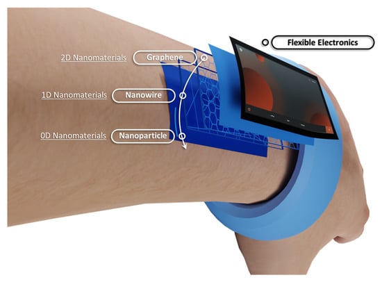
Hence, this section will provide a brief introduction to low-dimensional materials and their applications in flexible electronics.
Before discussing low-dimensional materials and their artificial synapses applications in detail, Table 1 provides a brief summary of the advantages and disadvantages of low-dimensional materials.
Table 1. Summary of the advantages and disadvantages of low-dimensional materials in the applications of flexible artificial synapses.
2.1. Zero Dimensional Materials
0D materials are the group of materials that have all three dimensions less than 100 nm, such as nanoclusters, quantum dots (QDs), and nanoparticles [
48]. Changes in spatial structure, morphology, size, and other parameters of 0D materials will lead to versatility in their physical and chemical properties [
49]. Due to their unique electrical and optical properties and their tuning properties, 0D materials have been widely employed in various electronic devices, including flexible artificial synapses [
50,
51,
52].
The performance of both memristors and transistors can be enhanced with the outstanding properties of 0D materials [
51,
53,
54]. For the application in memristors, conductive or semiconductive QDs were frequently used as the charge-trapping materials to increase uniformity in the performance of resistive switching among different cycles [
55]. Chen reported a MgO-graphene oxide quantum dot hybrid film with a solution processed method. The device exhibited highly controllable RS behavior, due to the enhancement of the local electric field by QD and the redox of QD under an electric field, and the basic synaptic behavior could be emulated [
53,
56]. For the application in synaptic transistors, conductive or semiconductive QDs can be embedded in the charge trapping layer or the dielectric/semiconductor interface of the transistor to store the charges. As a result, the synaptic characteristics can be mimicked. For example, Meng reported a synaptic transistor with a 2D MoSe channel and an 0D BPQD trap layer. The device had low power consumption of 0.86 fJ/spike and was able to emulate the classical conditioning of Pavlov’s dog [
51,
55]. In addition to the improvement in the electrical performance, the optical properties of the materials could make the artificial synapse responsive to both electrical and optical signals, which contributed to the advancement of optoelectronic synapses for neuromorphic electronics and artificial intelligence.
2.2. One-Dimensional Materials
Conductors, semiconductors, and insulators are three basic categories of materials, classified on the basis of their bandgaps or conductivity, for the fabrication of electronic devices. Conventional bulk materials with outstanding electrical properties are less useful in flexible electronics, which is desired for wearable systems, due to their brittleness and rigidity. By contrast, 1D nanomaterials, a group of low-dimensional materials, have been widely studied. For instance, conductive and semiconductor nanowires are used for the electrodes and channels, respectively, of synaptic transistors [
57]. The memristor can be fabricated with various nanowires [
58,
59].
Metal nanowires, such as Ag nanowire (AgNW), are typical conductive nanowires used in flexible electronics, due to their excellent mechanical deformability, high conductivity with less than 20 Ω/sq, and high transparency with a transmittance of 85% [
60]. In addition to their employment in drain/source/gate electrodes of transistors, AgNW is also widely employed in flexible and wearable sensors [
66]. Carbon nanotube (CNT), another typical nanowire, exhibits conductor and semiconductor properties, depending on its structure [
61]. In particular, the conductor-type CNT shows high conductivity and excellent mechanical deformability, due to the high aspect ratio of its structural characteristics [
67]. In addition, the electrochemical properties can be modified according to requirements through a wide range of functional groups. This phenomenon is beneficial for the fabrication of memristive devices, whose working mechanism is based on the trapping/detrapping of the carriers [
23]. However, if high transparency is also required, the layer of the conduction network should be carefully controlled, as a monolayer or a few layers [
68]. In addition, metal nanowires can be used in memristors when they are decorated with other materials, such as some polymers [
69].
Semiconductor-type nanowire is an indispensable component in flexible electronics, especially for transistor-based devices. Conventional semiconductor-based nanowires, such as silicon, germanium, and other compound semiconductor nanowires, have been widely studied, due to their excellent chemical stability, optical properties, and compatability with complementary metal oxide semiconductor (CMOS) technology. Kim et al. reported on an InGaAs nanowires-based field effect transistor (FET), which shows high stability and low variation in threshold voltage shift [
63]. Apart from conventional semiconductor nanowires, metal-oxide nanowires have attracted great attention due to the convenient synthesis method [
63,
70]. As previously reported, most metal-oxide nanowires can be synthesized by either hydrothermal or chemical vapor deposition (CVD) methods [
71,
72,
73]. For example, Hong et al. synthesized zinc oxide (ZnO) nanowires by the CVD method and fabricated the ZnO-based FETs by transferring the nanowire to a pre-prepared substrate [
62]. Both enhancement- and depletion-mode transistors were fabricated by tuning the diameter of the ZnO nanowires. Hence, the fabrication of flexible transistors with 1D materials provides a possible solution for the construction of transistor-type artificial synapses and corresponding neuromorphic systems [
16]. Some semiconductor nanowires, such as Si nanowire and ZnO nanowire, can also be used as resistive layers of memristor devices [
74,
75].
Insulator nanowires, synthesized on the basis of metal-oxide materials, are widely used in memristor devices due to the wide bandgap, although semiconductor nanowires and decorated metal nanowires can also be used as the resistive layer of a memristor [
58]. Compared with conventional memristors that are based on bulk metal-oxide insulators requiring a high working voltage and exhibiting rigidity in morphology, flexible memristors with a low working voltage can be fabricated with nanowire materials. Sun reported on the SiO
2 nanowire with a soft break phenomenon, indicating that nanowires can be used to fabricate memristor devices [
65]. Shan investigated a vertical-structure memristor based on TiO
2 nanowires, which implied that the fundamental synaptic characteristic can be emulated [
64].
2.3. Two-Dimensional Materials
Since the thickness of the material is one of the dominant factors for the flexibility of the devices, 2D materials with one or a few layers of atoms have a great advantage in the fabrication of flexible devices [
76]. Therefore, a number of 2D materials have been employed in the design and fabrication of flexible devices, based on their properties.
Graphene, a carbon allotrope composed of one layer of carbon atoms, was the first reported 2D material [
37]. Although graphene transistors’ low on/off ratio, attributed to its gapless band structure, hinders its applications in digital devices, its high carrier mobility of up to 250,000 cm
2 V
−1 s
−1 contributes to its application in analog devices and electrochemical sensors [
84]. In addition, its mechanical flexibility and outstanding Young’s modulus, due to strong atomic bonding, provide a foundation for the fabrication of flexible electronics [
77]. In addition to graphene, graphene oxide (GO) shows a number of advantages in memristive devices and chemical sensors, due to the plethora of functional groups [
23].
TMDs, a group of 2D materials with a non-zero bandgap, obtain tunable electrical and physical properties by various methods, such as defect engineering, electrostatic doping, and chemical intercalation [
43,
85,
86], which contribute to modifying the performance of FETs when TMDs are employed as the channel materials. MoS
2, a representative 2D material with high mobility and a suitable bandgap, is one of the most widely studied 2D materials recently. For example, MoS
2 FETs with low-threshold voltage shift, free hysteresis, and long-term reliability under bias were reported, involving the dielectrics’ optimal deposition and passivation methods [
78]. Moreover, benefiting from the atomic thickness of 2D materials, memristors with ultra-low voltage at several hundred millivoltages, called atomristors, can be achieved [
79,
87]. Although the underlying mechanism for the memristive behavior is unclear, this device provides a novel approach to constructing low-power neuromorphic devices. Taking advantage of the atomic thin property and free-standing nature of the 2D materials, a wide range of van der Waals heterostructures can be obtained by stacking various individual layers on top of each other without the constraints of lattice matching and processing compatibility. The heterostructure shows superior performances in optical, electrical, and electrochemical properties than those of single 2D materials. Yang reported a Cu
9S
5/PtS
2/WSe
2 double-heterojunction bipolar transistor with an excellent current gain (β ≈ 910) [
80]. Kim studied a heterojunction FET by engineering the band structure, and a low threshold swing of about 22 mV/dec was obtained, which paved the way for applications in low-power devices [
88].
In addition to conventional carbon-based 2D materials and TMDs, some novel 2D materials, such as MXene and perovskite, have been reported and employed in flexible electronics. For example, benefiting from its excellent mechanical, electrical, chemical, and physical properties and its hydrophilic surface, MXene has been widely used in energy storage, nanocomposite fabrication, and chemical sensing [
89,
90,
91]. Xu fabricated a label-free MXene-FET using ultrathin-conductive Ti
3C
2-MXene micropatterns for detecting dopamine, and a temporal resolution of ≈50 ms for neural activity was obtained [
81]. In addition, perovskite and other novel 2D materials were investigated in the application of electronic devices, although the long-term stability in ambient conditions still needs further improvement [
82,
83].