Large-Strain-Extrusion Machining: History
Please note this is an old version of this entry, which may differ significantly from the current revision.

Bulk nanostructured metals and alloys are finding increasing structural applications due to their superior mechanical properties. The methods that rely on the severe plastic deformation technique for effecting microstructural refinement through imposing large strains are utilized mostly to produce nanostructured materials. The machining process has been demonstrated as a simple process for severe plastic deformation by imposing large strains through a single pass of the cutting tool where strains in a range of 1–15 can be imposed for a variety of materials by varying the cutting conditions and tool geometry. However, the geometry of the resulting chip subjected to severe plastic deformation during the machining process is not under control and, hence, a variant of the machining process, called the large-strain-extrusion machining process, has been proposed and utilized extensively for producing bulk nanostructured materials. Large-strain-extrusion machining possesses simultaneous control over microstructure refinement, through managing the strain during large-strain machining, and the shape and dimension of the resulting chip by the extrusion process.

  • severe plastic deformation
  • large-strain-extrusion machining
  • ultra-fine-grain materials

1. Introduction

The presence of submicron-size grains in nanostructured materials provides them with some novel attributes compared to the conventional materials [1,2]. The level of microstructure refinement attained by varying the grain size has a greater impact on these novel characteristics of higher hardness, strength, ductility, and difference in electrical and magnetic properties [1,3,4]. Further superplasticity has also been observed in these nanostructured materials at relatively low temperatures [5,6]. Though nanostructured materials possess more benefits compared to conventional materials, they are not widely utilized for many applications due to the cost involved in the production process. Severe plastic deformation (SPD) in large-strain deformation has been increasingly utilized as a method to produce bulk nanostructured materials through microstructure refinement, effected by reductions in the grain size due to the imposition of large strains [7,8,9]. In this regard, the conventional manufacturing processes involving large-scale deformation, such as rolling, drawing, equal channel angular extrusion (ECAE), or high-pressure torsion, has been utilized. However, multiple passes are required in these SPD processes to impose very high strains of more than 4 with each pass effecting a strain of approximately 1 [10]. Further, these SPD processes are not suitable for high-strength metals and alloys in imposing large strains and, mostly, this SPD approach is restricted to produce nanostructured bulk material from low- to medium-strength ductile metal and alloys [8]. Further, these SPD techniques require multiple passes to impose high strain and, hence, the large-scale production of bulk nano-structured materials is cumbersome and expensive. In order to overcome these difficulties machining, was explored as an SPD technique since the chips produced during machining were found to have nano-crystalline structures, as they are subjected to very large shear strains [11].
Machining is a manufacturing process where excess material is removed from the workpiece to produce a finished component, with the desired dimensions and surface finish. It is a three-dimensional process, as shown in Figure 1, where a cutting tool with a sharp cutting edge would move longitudinally at a feed of (f) relative to the revolving workpiece, hence, reducing the diameter of the workpiece by the depth of cut (to) while the workpiece revolves at a certain rotational speed corresponding to a linear cutting velocity of V. It should be noted that the metal cutting process shown in Figure 1 is called turning, which is a classic representation of oblique or three-dimensional processes.
Figure 1. Schematic representation of machining process.
In machining, the work material is subjected to large values of strain in the order of 1 to 10 and strain rates of up to 106/s and temperatures in a range of 0.1 to 0.7 Tm (melting temperature) in a narrow cutting zone called the shear plane [12,13,14], as shown in Figure 2. The machining process is capable of imposing large values of strain and strain rate in a single pass, which is significantly higher than the strain and strain rate values that can be achieved, even through multiple stages of deformation using other SPD processes. Thus, machining has been utilized as an SPD technique to produce fine-grain materials from various metals and alloys [15]. A range of strain and strain rate values can be imposed in the machining process by altering the machining parameters, but since it is an unconstrained deformation process, it does not have control over shape and dimensions of the chip that is being cut from the work material [15]. In this regard, a constrained machining process, called large-strain-extrusion machining (LSEM), has been developed and explored as an SPD technique for producing bulk fine-structured materials with predefined geometry from various metals and alloys [16].
Figure 2. Schematic of orthogonal machining process.

2. Large-Strain-Extrusion Machining

LSEM is a constrained machining operation for obtaining a chip that has ultrafine-grain microstructure with a controlled shape and size. This process is carried out either through an orthogonal cutting or a conventional turning approach, with certain modifications in the tool and fixtures. Smaller strips are obtained when the orthogonal cutting configuration is implemented, as shown in Figure 3, and continuous chips are possible when the turning approach is utilized.
Figure 3. Schematic of large-strain-extrusion machining [22].

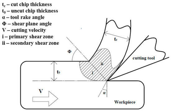
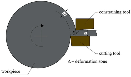
2.1. LSEM through Orthogonal Cutting

The basic functionality of both LSEM configurations remains the same. The only difference comes in the geometry of the machined chip. A schematic of the LSEM process through the orthogonal cutting procedure is shown in Figure 3. It consists of a cutting tool with a rake angle α and a constraining tool that controls the shape of the chip, which is being extruded with a thickness tc. This process is very similar to the orthogonal cutting process but with control over the shape and thickness of the chip. Gurusamy et al. [22] and Palaiappan et al. [23] conducted LSEM experiments through this method by using a Computer Numeric Control (CNC) milling machine with a custom-made tool and fixture for producing UFG chips of Inconel 718 and Ti-6Al-4V, respectively, as shown in Figure 4, Figure 5 and Figure 6.
Figure 4. Cutting tool dimensions [22].
Figure 5. LSEM fixture dimensions [22].
Figure 6. LSEM setup [22].

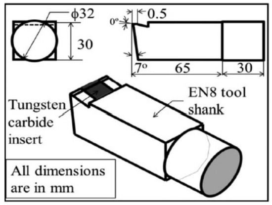
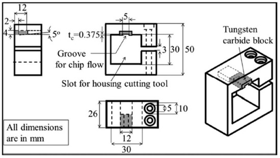
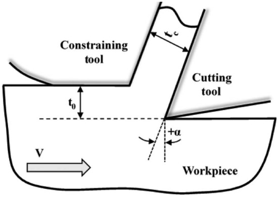
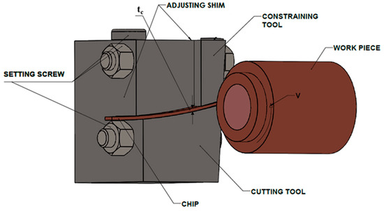
Cutting Tool and LSME Fixture

As shown in Figure 4 and Figure 5, a single-edge cutting tool and specially designed LSEM fixture were utilized for LSEM experiments by Palaniappan et al. [23]. Figure 5 provides details of the cutting tool utilized for the LSEM experiment with EN8 steel used for the tool shank, which is brazed to a Tungsten Carbide (WC-Co) insert with a defined rake and clearance angle of 0° and 7°. To avoid the effect of friction along the tool–chip interface, a restricted contact length of 0.5 mm is provided on the tungsten carbide insert, as shown in Figure 4 and Figure 5. Palaniappan et al. [23] designed an LSEM fixture specifically for orthogonal cutting, as per the dimensions shown in Figure 5. The LSEM fixture shown in Figure 5 has a tungsten carbide block of higher hardness brazed in the inner region where the chip extrudes. It helps avoid the erosion of the inner surface of the groove, as extrusion occurs due to the higher hardness of chip material compared to the EN8 utilized for manufacturing the LSEM fixture.
In our previous efforts [22,23], we were able to produce UFG foils of Ti-6Al-4V and Inconel 718 through LSEM experiments conducted using the orthogonal cutting approach. The extruded foils of Ti-6Al-4V and Inconel 718 had superior mechanical properties compared to the bulk material.

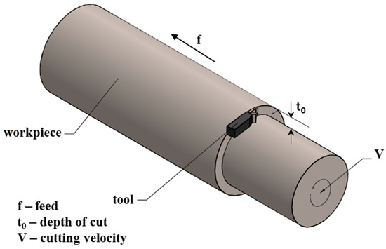
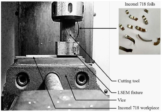
2.2. LSEM through Turning Experiment

The only limitation of LSEM through the orthogonal cutting configuration is that the continuous UFG strips or foils cannot be produced since the feed is restricted to the length of the workpiece. To overcome this shortcoming, a turning methodology is followed where the tool moves over a disc-shaped workpiece rotating at a constant speed V (m/s).
This setup also consists of two components, a single-point cutting tool with rake angle α and a wedge shape constraining part, as shown in Figure 7, which is made of a harder material. Because of the intense cutting pressure experienced during LSEM, the inner surface of the constraining part might be eroded. Hence, tungsten carbide inserts are brazed onto the inner side of the constraint tool or the whole constraining part should be made of a harder material similar to the cutting tool [23]. The tool radially advances at a constant feed rate t where the undeformed material is fed continuously in the machining zone. The velocity of the chip at the exit during the LSEM process is given by Vc = Vt0/tc, where tc is the cut chip thickness and t0 is the uncut chip thickness. Shear strain is purely dependent on rake angle α and chip thickness ratio (λ) where λ = tc/t0. Shear strain (γ) is given by,
γ = λ cos α + 1 λ cos α + 2 tan α
Figure 7. Schematic of turning approach in LSEM experiment.
The turning experiment of LSEM is either carried out on hollow cylindrical tubes or solid cylindrical tubes [24,25,26]. Hollow tubes made of pure copper and solid tubes made of low-carbon steel are machined through the LSEM experimental setup, as shown in Figure 8 [27,28]. In the LSEM experimental setup shown in Figure 8, both cut and uncut chip thickness can be controlled by adjusting the screws provided. In order to minimize the effect of shear strain and temperature on the extruded chip, the cutting velocity is maintained at a low level [27,28].
Figure 8. Turing-based LSEM experimental setup.

2.3. Advantages of LSEM Process over Other SPD Processes

Equal-channel angular pressing (ECAP) is a conventional SPD process, as mentioned in Section 1, and it requires at least four passes to produce ultrafine-grain structures. In this regard, the time consumed by an ECAP process is higher compared to that of an LSEM process and, hence, the carbon footprint generated in ECAP is higher due to the larger machine run-time. In large-strain-extrusion machining, a single cut is enough for producing UFG foils or strips and, thus, reduces the energy consumption, which, in turn, translates to lesser carbon footprint deposition. In the LSEM process, UFG foils of different shapes with varying diameters can be achieved by modifying the fixture design. The nano-structured ribbons obtained from the LSEM process and other SPD have enhanced magnetic and electrical properties due to the assembly of organic structures. These UFG materials can be used in fabricating nanoelectromechanical systems (NEMSs) [25]. When the material is extruded in the shape of a wire or a rod, it can also be used as a core for multifunctional batteries. Machining of certain metals and alloys produces a shear localized chip, which, in turn, leads to larger tool wear, improper surface finish, and machine tool vibrations, which might lead to higher resource and energy consumption. Shear localization occurs when the rate of decrease in strength due to thermal softening exceeds the rate of increase in strength due to strain hardening. LSEM is a single-step plane-strain deformation process that combines large plastic strains of machining with a dimensional control of the chip due to extrusion. The chip is simultaneously forced to flow through the gap between the constraining edge and the rake surface of the cutting tool, thereby affecting the chip geometry to form a foil and, thus, helping to suppress shear localization. As a result, complete control of the deformation parameters, such as strain, strain rate, temperature, shape, and size of the grain, is possible through this combination of extrusion and machining processes [25].
Chatter is another important parameter to take into consideration when the quality of the finished product and energy consumed during machining are important. Serrated chips mostly give rise to vibrations, which might result in chatter. The LSEM process suppresses shear localization and produces continuous chips, which eventually ends up reducing the chatter [25].
 

LSEM as Frugal Process

The exploitation of Earth’s limited resources through human activities has led to a severe scarcity of resources and issues of climate change. In this regard, it is high time to adopt sustainability principles for all-round sustainable development, which would help in improving the standard of living and also allow the earth to prosper and be maintained [107]. Sustainable innovations are the need of the hour, as suggested by Boons et al. [108], for both economic and environmental upheaval. In this regard, advances in science and technology are required for frugal manufacturing, which will reduce cost and resource consumption [109]. Frugality through resource optimization is an important pillar for sustainable development [110]. Rao [111] examined the disruptive nature of frugal innovations by studying various examples of frugal innovations in different sectors. The frugal products are manufactured with minimal resources at low cost but they exhibit better functionalities compared to conventional types and, in recent years, they have started proliferating the market, which is a sign of moving towards sustainable development [112,113,114,115,116]. The manufacturing process plays an important role by providing proper inputs to frugal design and, further, for the fabrication of frugal products. Therefore, there is a need to conceptualize and implement a frugal manufacturing process [117]. Rao [118] defined the concept of frugal manufacturing as a fabrication activity utilizing a minimal number of processes at low cost without any compromise on surface integrity and other appropriate properties.
Mann et al. [119] studied the demonstrated capabilities of the LSEM process and proposed that it is an attractive machining-based process for producing bulk forms, such as foils, sheets, wires, and strips, in a low-cost energy-efficient method because of its characteristic features. LSEM, as single-step SPD process, has the capability to produce bulk forms of sheet, foil, strip, and wire, even from low-machinability alloys with varying UFG microstructure and crystallographic texture using a compact and economical infrastructure. Therefore, LSEM could be considered as a frugal manufacturing process since it helps in reducing waste through recycling the chip and it is also a single-step energy-efficient process.

This entry is adapted from the peer-reviewed paper 10.3390/cryst13010131

References

  1. Arnold, M. Fostering sustainability by linking co-creation and relationship management concepts. J. Clean. Prod. 2017, 140, 179–188. [Google Scholar] [CrossRef]
  2. Boons, F.; Montalvo, C.; Quist, J.; Wagner, M. Sustainable innovation, business models and economic performance: An overview. J. Clean. Prod. 2013, 45, 1–8. [Google Scholar] [CrossRef]
  3. Rao, B.C. Advances in science and technology through frugality. IEEE Eng. Manag. Rev. 2017, 45, 32–38. [Google Scholar] [CrossRef]
  4. Hoekstra, A.Y.; Wiedmann, T.O. Humanity’s unsustainable environmental footprint. Science 2014, 344, 1114–1117. [Google Scholar] [CrossRef]
  5. Rao, B.C. How disruptive is frugal? Technol. Soc. 2013, 35, 65–73. [Google Scholar] [CrossRef]
  6. Zeschky, M.; Widenmayer, B.; Gassmann, O. Frugal Innovation in Emerging Markets: The Case of Mettler Toledo. Res. Technol. Manag. 2011, 54, 38–45. [Google Scholar] [CrossRef]
  7. Tiwari, R.; Herstatt, C. Open Global Innovation Networks as Enablers of Frugal Innovation: Propositions Based on Evidence from India; Working Paper No. 72; Hamburg University of Technology, Technology and Innovation Management: Hamburg, Germany, 2012. [Google Scholar]
  8. Knorringa, P.; Peša, I.; Leliveld, A.; Van Beers, C. Frugal innovation and development: Aides or adversaries? Eur. J. Dev. Res. 2016, 28, 143–153. [Google Scholar] [CrossRef]
  9. Prabhu, J. Frugal innovation: Doing more with less for more. Philos. Trans. R. Soc. A Math. Phys. Eng. Sci. 2017, 375, 20160372. [Google Scholar] [CrossRef]
  10. Rao, B.C. The science underlying frugal innovations should not be frugal. R. Soc. Open Sci. 2019, 6, 180421. [Google Scholar] [CrossRef] [PubMed]
  11. Rao, B.C. Revisiting classical design in engineering from a perspective of frugality. Heliyon 2017, 3, e00299. [Google Scholar] [CrossRef] [PubMed]
  12. Rao, B.C. Frugal manufacturing in smart factories for widespread sustainable development. R. Soc. Open Sci. 2021, 8, 210375. [Google Scholar] [CrossRef] [PubMed]
  13. Mann, J.B.; Saei, M.; Udupa, A.; Puentes-Rodriguez, B.S.; Sagapuram, D. Applications of Machining in Materials Manufacturing. In International Manufacturing Science and Engineering Conference; American Society of Mechanical Engineers: New York, NY, USA, 2020; Volume 84256, p. V001T05A008. [Google Scholar]
  14. Shaw, M.C. Metal Cutting Principles; Clarendon: Oxford, UK, 1984; p. 32. [Google Scholar]
  15. Swaminathan, S.; RaviShankar, M.; Lee, S.; Hwang, J.; King, A.H.; Kezar, R.F.; Rao, B.C.; Brown, T.L.; Chandrasekar, S.; Compton, W.D.; et al. Large Strain Deformation and Ultrafine Grained Materials by Machining. Mater. Sci. Eng. A 2005, 410–411, 358–363. [Google Scholar] [CrossRef]
  16. Moscoso, W.; Ravi Shankar, M.; Mann, J.B.; Compton, W.D.; Chandrasekar, S. Bulk Nanostructured Materials by Large Strain Extrusion Machining. J. Mater. Res. 2007, 22, 201–205. [Google Scholar] [CrossRef]
  17. Liu, Y.; Cai, S.; Xu, F.; Wang, Y.; Dai, L. Enhancing strength without compromising ductility in copper by combining extrusion machining and heat treatment. J. Mater. Process. Technol. 2019, 267, 52–60. [Google Scholar] [CrossRef]
  18. Cai, S.L.; Chen, Y.; Ye, G.G.; Jiang, M.Q.; Wang, H.Y.; Dai, L.H. Characterization of the deformation field in large-strain extrusion machining. J. Mater. Process. Technol. 2015, 216, 48–58. [Google Scholar] [CrossRef]
  19. Guo, Y.A.N.G.; Efe, M.; Moscoso, W.; Sagapuram, D.; Trumble, K.P.; Chandrasekar, S. Deformation field in large-strain extrusion machining and implications for deformation processing. Scr. Mater. 2012, 66, 235–238. [Google Scholar] [CrossRef]
  20. Guo, Y.; Chen, J.; Saleh, A. In situ analysis of deformation mechanics of constrained cutting toward enhanced material removal. J. Manuf. Sci. Eng. 2020, 142, 021002. [Google Scholar] [CrossRef]
  21. Efe, M.; Moscoso, W.; Trumble, K.P.; Compton, W.D.; Chandrasekar, S. Mechanics of large strain extrusion machining and application to deformation processing of magnesium alloys. Acta Mater. 2012, 60, 2031–2042. [Google Scholar] [CrossRef]
  22. Gurusamy, M.; Palaniappan, K.; Murthy, H.; Rao, B.C. A Finite Element Study of Large Strain Extrusion Machining Using Modified Zerilli–Armstrong Constitutive Relation. J. Manuf. Sci. Eng. 2021, 143, 101004. [Google Scholar] [CrossRef]
  23. Palaniappan, K.; Murthy, H.; Rao, B.C. Production of fine-grained foils by large strain extrusion-machining of textured Ti–6Al–4V. J. Mater. Res. 2018, 33, 108–120. [Google Scholar] [CrossRef]
  24. Deng, W.J.; Lin, P.; Li, Q.; Xia, W. Effect of constraining tool corner radius on large strain extrusion machining. Mater. Manuf. Process. 2013, 28, 1090–1094. [Google Scholar] [CrossRef]
  25. Moscoso, W. Severe Plastic Deformation and Nanostructured Materials by Large Strain Extrusion Machining. Ph.D. Thesis, Purdue University, West Lafayette, IN, USA, 2008. [Google Scholar]
  26. Arnold, M. Fostering sustainability by linking co-creation and relationship management concepts. J. Clean. Prod. 2017, 140, 179–188. [Google Scholar] [CrossRef]
  27. Boons, F.; Montalvo, C.; Quist, J.; Wagner, M. Sustainable innovation, business models and economic performance: An overview. J. Clean. Prod. 2013, 45, 1–8. [Google Scholar] [CrossRef]
  28. Rao, B.C. Advances in science and technology through frugality. IEEE Eng. Manag. Rev. 2017, 45, 32–38. [Google Scholar] [CrossRef]
  29. Hoekstra, A.Y.; Wiedmann, T.O. Humanity’s unsustainable environmental footprint. Science 2014, 344, 1114–1117. [Google Scholar] [CrossRef]
  30. Rao, B.C. How disruptive is frugal? Technol. Soc. 2013, 35, 65–73. [Google Scholar] [CrossRef]
  31. Zeschky, M.; Widenmayer, B.; Gassmann, O. Frugal Innovation in Emerging Markets: The Case of Mettler Toledo. Res. Technol. Manag. 2011, 54, 38–45. [Google Scholar] [CrossRef]
  32. Tiwari, R.; Herstatt, C. Open Global Innovation Networks as Enablers of Frugal Innovation: Propositions Based on Evidence from India; Working Paper No. 72; Hamburg University of Technology, Technology and Innovation Management: Hamburg, Germany, 2012. [Google Scholar]
  33. Knorringa, P.; Peša, I.; Leliveld, A.; Van Beers, C. Frugal innovation and development: Aides or adversaries? Eur. J. Dev. Res. 2016, 28, 143–153. [Google Scholar] [CrossRef]
  34. Prabhu, J. Frugal innovation: Doing more with less for more. Philos. Trans. R. Soc. A Math. Phys. Eng. Sci. 2017, 375, 20160372. [Google Scholar] [CrossRef]
  35. Rao, B.C. The science underlying frugal innovations should not be frugal. R. Soc. Open Sci. 2019, 6, 180421. [Google Scholar] [CrossRef] [PubMed]
  36. Rao, B.C. Revisiting classical design in engineering from a perspective of frugality. Heliyon 2017, 3, e00299. [Google Scholar] [CrossRef] [PubMed]
  37. Rao, B.C. Frugal manufacturing in smart factories for widespread sustainable development. R. Soc. Open Sci. 2021, 8, 210375. [Google Scholar] [CrossRef] [PubMed]
  38. Mann, J.B.; Saei, M.; Udupa, A.; Puentes-Rodriguez, B.S.; Sagapuram, D. Applications of Machining in Materials Manufacturing. In International Manufacturing Science and Engineering Conference; American Society of Mechanical Engineers: New York, NY, USA, 2020; Volume 84256, p. V001T05A008. [Google Scholar]
More
This entry is offline, you can click here to edit this entry!
ScholarVision Creations