Single-element-based 2D materials (Xenes) have garnered tremendous interest. At present, 16 kinds of Xenes (silicene, borophene, germanene, phosphorene, tellurene, etc.) have been explored, mainly distributed in the third, fourth, fifth, and sixth main groups. Although two Xenes (aluminene and indiene) have not been synthesized due to the limitations of synthetic methods and the stability of Xenes, other Xenes have been successfully created via elaborate artificial design and synthesis. Elemental 2D materials show potential applications in various fields, including spintronics, electronics, optoelectronics, superconducting, photovoltaics, sensors, catalysis, and biomedicines.
- elemental two-dimensional materials
- allotropic structures
- synthesis methods
- applications
1. Introduction
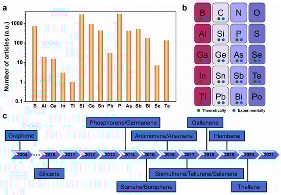
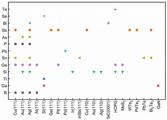
2. Classification of 2D Xenes
3. Applications of 2D Xenes
This entry is adapted from the peer-reviewed paper 10.3390/molecules28010200
References
- Novoselov, K.S.; Geim, A.K.; Morozov, S.V.; Jiang, D.‑e.; Zhang, Y.; Dubonos, S.V.; Grigorieva, I.V.; Firsov, A.A. Electric field effect in atomically thin carbon films. Science 2004, 306, 666–669.
- Mannix, A.J.; Kiraly, B.; Hersam, M.C.; Guisinger, N.P. Synthesis and chemistry of elemental 2D materials. Nat. Rev. Chem. 2017, 1, 0014.
- Kis, A. Graphene is not alone. Nat. Nanotechnol. 2012, 7, 683.
- Butler, S.Z.; Hollen, S.M.; Cao, L.; Cui, Y.; Gupta, J.A.; Gutiérrez, H.R.; Heinz, T.F.; Hong, S.S.; Huang, J.; Ismach, A.F. Progress, challenges, and opportunities in two‑dimensional materials beyond graphene. ACS Nano 2013, 7, 2898–2926.
- Xiao, X.; Song, H.; Lin, S.; Zhou, Y.; Zhan, X.; Hu, Z.; Zhang, Q.; Sun, J.; Yang, B.; Li, T. Scalable salt‑templated synthesis of two‑dimensional transition metal oxides. Nat. Commun. 2016, 7, 11296.
- Huang, B.; Clark, G.; Navarro‑Moratalla, E.; Klein, D.R.; Cheng, R.; Seyler, K.L.; Zhong, D.; Schmidgall, E.; McGuire, M.A.; Cobden, D.H. Layer‑dependent ferromagnetism in a van der Waals crystal down to the monolayer limit. Nature 2017, 546, 270–273.
- Burch, K.S.; Mandrus, D.; Park, J.‑G. Magnetism in two‑dimensional van der Waals materials. Nature 2018, 563, 47–52.
- Zhang, Y.‑Z.; El‑Demellawi, J.K.; Jiang, Q.; Ge, G.; Liang, H.; Lee, K.; Dong, X.; Alshareef, H.N. MXene hydrogels: Fundamentals and applications. Chem. Soc. Rev. 2020, 49, 7229–7251.
- Zhang, C.J.; McKeon, L.; Kremer, M.P.; Park, S.‑H.; Ronan, O.; Seral‑Ascaso, A.; Barwich, S.; Coileáin, C.Ó.; McEvoy, N.; Nerl, H.C. Additive‑free MXene inks and direct printing of micro‑supercapacitors. Nat. Commun. 2019, 10, 1795.
- Novoselov, K.; Mishchenko, O.A.; Carvalho, O.A.; Castro Neto, A. 2D materials and van der Waals heterostructures. Science 2016, 353, aac9439.
- Li, L.; Kim, J.; Jin, C.; Ye, G.J.; Qiu, D.Y.; Da Jornada, F.H.; Shi, Z.; Chen, L.; Zhang, Z.; Yang, F. Direct observation of the layer‑dependent electronic structure in phosphorene. Nat. Nanotechnol. 2017, 12, 21–25.
- Ma, Y.; Shao, X.; Li, J.; Dong, B.; Hu, Z.; Zhou, Q.; Xu, H.; Zhao, X.; Fang, H.; Li, X. Electrochemically exfoliated platinum dichalcogenide atomic layers for high‑performance air‑stable infrared photodetectors. ACS Appl. Mater. Interfaces 2021, 13, 8518–8527.
- Hasan, M.Z.; Kane, C.L. Colloquium: Topological insulators. Rev. Mod. Phys. 2010, 82, 3045.
- Konig, M.; Wiedmann, S.; Brune, C.; Roth, A.; Buhmann, H.; Molenkamp, L.W.; Qi, X.‑L.; Zhang, S.‑C. Quantum spin Hall insulator state in HgTe quantum wells. Science 2007, 318, 766–770.
- Kane, C.L.; Mele, E.J. Quantum spin Hall effect in graphene. Phys. Rev. Lett. 2005, 95, 226801.
- Liu, C.‑C.; Feng, W.; Yao, Y. Quantum spin Hall effect in silicene and two‑dimensional germanium. Phys. Rev. Lett. 2011, 107, 076802.
- Schaibley, J.R.; Yu, H.; Clark, G.; Rivera, P.; Ross, J.S.; Seyler, K.L.; Yao, W.; Xu, X. Valleytronics in 2D materials. Nat. Rev. Mater. 2016, 1, 16055.
- Castellanos‑Gomez, A. Why all the fuss about 2D semiconductors? Nat. Photonics 2016, 10, 202–204.
- Xu, M.; Liang, T.; Shi, M.; Chen, H. Graphene‑like two‑dimensional materials. Chem. Rev. 2013, 113, 3766–3798.
- Aufray, B.; Kara, A.; Vizzini, S.; Oughaddou, H.; Léandri, C.; Ealet, B.; Le Lay, G. Graphene‑like silicon nanoribbons on Ag (110): A possible formation of silicene. Appl. Phys. Lett. 2010, 96, 183102.
- Dávila, M.; Xian, L.; Cahangirov, S.; Rubio, A.; Le Lay, G. Germanene: A novel two‑dimensional germanium allotrope akin to graphene and silicene. New J. Phys. 2014, 16, 095002.
- Mannix, A.J.; Zhou, X.‑F.; Kiraly, B.; Wood, J.D.; Alducin, D.; Myers, B.D.; Liu, X.; Fisher, B.L.; Santiago, U.; Guest, J.R. Synthesis of borophenes: Anisotropic, two‑dimensional boron polymorphs. Science 2015, 350, 1513–1516.
- Li, L.; Yu, Y.; Ye, G.J.; Ge, Q.; Ou, X.; Wu, H.; Feng, D.; Chen, X.H.; Zhang, Y. Black phosphorus field‑effect transistors. Nat. Nanotechnol. 2014, 9, 372–377.
- Zhang, S.; Yan, Z.; Li, Y.; Chen, Z.; Zeng, H. Atomically thin arsenene and antimonene: Semimetal–semiconductor and indirect–direct band‑gap transitions. Angew. Chem. 2015, 127, 3155–3158.
- Zhu, F.‑F.; Chen, W.‑J.; Xu, Y.; Gao, C.‑L.; Guan, D.‑D.; Liu, C.‑H.; Qian, D.; Zhang, S.‑C.; Jia, J.‑F. Epitaxial growth of two-dimensional stanene. Nat. Mater. 2015, 14, 1020–1025.
- Reis, F.; Li, G.; Dudy, L.; Bauernfeind, M.; Glass, S.; Hanke, W.; Thomale, R.; Schäfer, J.; Claessen, R. Bismuthene on a SiC substrate: A candidate for a high‑temperature quantum spin Hall material. Science 2017, 357, 287–290.
- Zhu, Z.; Cai, X.; Yi, S.; Chen, J.; Dai, Y.; Niu, C.; Guo, Z.; Xie, M.; Liu, F.; Cho, J.‑H. Multivalency‑driven formation of Te‑based monolayer materials: A combined first‑principles and experimental study. Phys. Rev. Lett. 2017, 119, 106101.
- Qin, J.; Qiu, G.; Jian, J.; Zhou, H.; Yang, L.; Charnas, A.; Zemlyanov, D.Y.; Xu, C.‑Y.; Xu, X.; Wu, W. Controlled growth of a large-size 2D selenium nanosheet and its electronic and optoelectronic applications. ACS Nano 2017, 11, 10222–10229.
- Kochat, V.; Samanta, A.; Zhang, Y.; Bhowmick, S.; Manimunda, P.; Asif, S.A.S.; Stender, A.S.; Vajtai, R.; Singh, A.K.; Tiwary, C.S. Atomically thin gallium layers from solid‑melt exfoliation. Sci. Adv. 2018, 4, e1701373.
- Yuhara, J.; He, B.; Matsunami, N.; Nakatake, M.; Le Lay, G. Graphene’s latest cousin: Plumbene epitaxial growth on a “nano WaterCube”. Adv. Mater. 2019, 31, 1901017.
- Liu, G.; Xu, S.‑G.; Ma, Y.; Shao, X.; Xiong, W.; Wu, X.; Zhang, S.; Liao, C.; Chen, C.; Wang, X. Arsenic Monolayers Formed by Zero‑Dimensional Tetrahedral Clusters and One‑Dimensional Armchair Nanochains. ACS Nano 2022, 16, 17087–17096.
- Yeoh, K.H.; Yoon, T.L.; Ong, D.S.; Lim, T.L. First‑principles studies on the superconductivity of aluminene. Appl. Surf. Sci. 2018, 445, 161–166.
- Hernandez, Y.; Nicolosi, V.; Lotya, M.; Blighe, F.M.; Sun, Z.; De, S.; McGovern, I.T.; Holland, B.; Byrne, M.; Gun’Ko, Y.K. High-yield production of graphene by liquid‑phase exfoliation of graphite. Nat. Nanotechnol. 2008, 3, 563–568.
- Yuan, J.; Yu, N.; Xue, K.; Miao, X. Stability, electronic and thermodynamic properties of aluminene from first‑principles calculations. Appl. Surf. Sci. 2017, 409, 85–90.
- Zhang, Z.; Yang, Y.; Gao, G.; Yakobson, B.I. Two‑dimensional boron monolayers mediated by metal substrates. Angew. Chem. 2015, 127, 13214–13218.
- Liu, Y.; Penev, E.S.; Yakobson, B.I. Probing the synthesis of two‑dimensional boron by first‑principles computations. Angew. Chem. Int. Ed. 2013, 52, 3156–3159.
- Huang, Y.; Shirodkar, S.N.; Yakobson, B.I. Two‑dimensional boron polymorphs for visible range plasmonics: A first‑principles exploration. J. Am. Chem. Soc. 2017, 139, 17181–17185.
- Singh, D.; Gupta, S.K.; Lukačević, I.; Sonvane, Y. Indiene 2D monolayer: A new nanoelectronic material. RSC Adv. 2016, 6, 8006–8014.
- Deng, J.; Xia, B.; Ma, X.; Chen, H.; Shan, H.; Zhai, X.; Li, B.; Zhao, A.; Xu, Y.; Duan, W. Epitaxial growth of ultraflat stanene with topological band inversion. Nat. Mater. 2018, 17, 1081–1086.
- Ren, W.; Cheng, H.‑M. The global growth of graphene. Nat. Nanotechnol. 2014, 9, 726–730.
- Sprinkle, M.; Ruan, M.; Hu, Y.; Hankinson, J.; Rubio‑Roy, M.; Zhang, B.; Wu, X.; Berger, C.; De Heer, W.A. Scalable templated growth of graphene nanoribbons on SiC. Nat. Nanotechnol. 2010, 5, 727–731.
- Meng, L.; Wang, Y.; Zhang, L.; Du, S.; Wu, R.; Li, L.; Zhang, Y.; Li, G.; Zhou, H.; Hofer, W.A. Buckled silicene formation on Ir(111). Nano Lett. 2013, 13, 685–690.
- Li, L.; Lu, S.Z.; Pan, J.; Qin, Z.; Wang, Y.q.; Wang, Y.; Cao, G.y.; Du, S.; Gao, H.J. Buckled germanene formation on Pt (111). Adv. Mater. 2014, 26, 4820–4824.
- Zhang, S.; Zhou, J.; Wang, Q.; Chen, X.; Kawazoe, Y.; Jena, P. Penta‑graphene: A new carbon allotrope. Proc. Natl. Acad. Sci. USA 2015, 112, 2372–2377.
- Wang, Z.; Zhou, X.‑F.; Zhang, X.; Zhu, Q.; Dong, H.; Zhao, M.; Oganov, A.R. Phagraphene: A low‑energy graphene allotrope composed of 5–6–7 carbon rings with distorted Dirac cones. Nano Lett. 2015, 15, 6182–6186.
- Matusalem, F.; Marques, M.; Teles, L.K.; Bechstedt, F. Stability and electronic structure of two‑dimensional allotropes of group‑IV materials. Phys. Rev. B 2015, 92, 045436.
- Guan, J.; Zhu, Z.; Tománek, D. Tiling phosphorene. ACS Nano 2014, 8, 12763–12768.
- Wu, X.; Shao, Y.; Liu, H.; Feng, Z.; Wang, Y.L.; Sun, J.T.; Liu, C.; Wang, J.O.; Liu, Z.L.; Zhu, S.Y. Epitaxial growth and air‑stability of monolayer antimonene on PdTe2. Adv. Mater. 2017, 29, 1605407.
- Lu, Y.; Xu, W.; Zeng, M.; Yao, G.; Shen, L.; Yang, M.; Luo, Z.; Pan, F.; Wu, K.; Das, T. Topological properties determined by atomic buckling in self‑assembled ultrathin Bi (110). Nano Lett. 2015, 15, 80–87.
- Carvalho, A.; Wang, M.; Zhu, X.; Rodin, A.S.; Su, H.; Castro Neto, A.H. Phosphorene: From theory to applications. Nat. Rev. Mater. 2016, 1, 16061.
- Aktürk, E.; Aktürk, O.Ü.; Ciraci, S. Single and bilayer bismuthene: Stability at high temperature and mechanical and electronic properties. Phys. Rev. B 2016, 94, 014115.
- Kamal, C.; Ezawa, M. Arsenene: Two‑dimensional buckled and puckered honeycomb arsenic systems. Phys. Rev. B 2015, 91, 085423.
- Mardanya, S.; Thakur, V.K.; Bhowmick, S.; Agarwal, A. Four allotropes of semiconducting layered arsenic that switch into a topological insulator via an electric field: Computational study. Phys. Rev. B 2016, 94, 035423.
- Xian, L.; Paz, A.P.; Bianco, E.; Ajayan, P.M.; Rubio, A. Square selenene and tellurene: Novel group VI elemental 2D materials with nontrivial topological properties. 2D Mater. 2017, 4, 041003.
- Sakaguchi, H.; Song, S.; Kojima, T.; Nakae, T. Homochiral polymerization‑driven selective growth of graphene nanoribbons. Nat. Chem. 2017, 9, 57–63.
- Ni, Z.; Ma, L.; Du, S.; Xu, Y.; Yuan, M.; Fang, H.; Wang, Z.; Xu, M.; Li, D.; Yang, J. Plasmonic silicon quantum dots enabled high-sensitivity ultra-broadband photodetection of graphene‑based hybrid phototransistors. ACS Nano 2017, 11, 9854–9862.
- Dang, Z.; Wang, W.; Chen, J.; Walker, E.S.; Bank, S.R.; Akinwande, D.; Ni, Z.; Tao, L. Vis‑NIR photodetector with microsecond response enabled by 2D bismuth/Si (111) heterojunction. 2D Mater. 2021, 8, 035002.
- Lin, S.; Liu, S.; Yang, Z.; Li, Y.; Ng, T.W.; Xu, Z.; Bao, Q.; Hao, J.; Lee, C.S.; Surya, C. Solution‑processable ultrathin black phosphorus as an effective electron transport layer in organic photovoltaics. Adv. Funct. Mater. 2016, 26, 864–871.
- Mayorga‑Martinez, C.C.; Sofer, Z.; Pumera, M. Layered black phosphorus as a selective vapor sensor. Angew. Chem. Int. Ed. 2015, 54, 14317–14320.
- Saito, Y.; Iizuka, T.; Koretsune, T.; Arita, R.; Shimizu, S.; Iwasa, Y. Gate‑tuned thermoelectric power in black phosphorus. Nano Lett. 2016, 16, 4819–4824.
- Kong, X.; Gao, M.; Yan, X.‑W.; Lu, Z.‑Y.; Xiang, T. Superconductivity in electron‑doped arsenene. Chin. Phys. B 2018, 27, 046301.
- Xu, Y.; Yan, B.; Zhang, H.‑J.; Wang, J.; Xu, G.; Tang, P.; Duan, W.; Zhang, S.‑C. Large‑gap quantum spin Hall insulators in tin films. Phys. Rev. Lett. 2013, 111, 136804.
- Yao, Y.; Fu, Q.; Zhang, Y.; Weng, X.; Li, H.; Chen, M.; Jin, L.; Dong, A.; Mu, R.; Jiang, P. Graphene cover‑promoted metal‑catalyzed reactions. Proc. Natl. Acad. Sci. USA 2014, 111, 17023–17028.
- Chang, K.; Mei, Z.; Wang, T.; Kang, Q.; Ouyang, S.; Ye, J. MoS2/graphene cocatalyst for efficient photocatalytic H2 evolution under visible light irradiation. ACS Nano 2014, 8, 7078–7087.
- Tao, W.; Kong, N.; Ji, X.; Zhang, Y.; Sharma, A.; Ouyang, J.; Qi, B.; Wang, J.; Xie, N.; Kang, C.; et al. Emerging two‑dimensional monoelemental materials (Xenes) for biomedical applications. Chem. Soc. Rev. 2019, 48, 2891–2912.
- Xue, T.; Bongu, S.R.; Huang, H.; Liang, W.; Wang, Y.; Zhang, F.; Liu, Z.; Zhang, Y.; Zhang, H.; Cui, X. Ultrasensitive detection of microRNA using a bismuthene‑enabled fluorescence quenching biosensor. Chem. Commun. 2020, 56, 7041–7044.
- Tao, W.; Ji, X.; Xu, X.; Islam, M.A.; Li, Z.; Chen, S.; Saw, P.E.; Zhang, H.; Bharwani, Z.; Guo, Z. Antimonene quantum dots: Synthesis and application as near‑infrared photothermal agents for effective cancer therapy. Angew. Chem. 2017, 129, 12058–12062.