A scanning transmission electron microscope (STEM) is a type of transmission electron microscope (TEM). Pronunciation is [stɛm] or [ɛsti:i:ɛm]. As with a conventional transmission electron microscope (CTEM), images are formed by electrons passing through a sufficiently thin specimen. However, unlike CTEM, in STEM the electron beam is focused to a fine spot (with the typical spot size 0.05 – 0.2 nm) which is then scanned over the sample in a raster illumination system constructed so that the sample is illuminated at each point with the beam parallel to the optical axis. The rastering of the beam across the sample makes STEM suitable for analytical techniques such as Z-contrast annular dark-field imaging, and spectroscopic mapping by energy dispersive X-ray (EDX) spectroscopy, or electron energy loss spectroscopy (EELS). These signals can be obtained simultaneously, allowing direct correlation of images and spectroscopic data. A typical STEM is a conventional transmission electron microscope equipped with additional scanning coils, detectors, and necessary circuitry, which allows it to switch between operating as a STEM, or a CTEM; however, dedicated STEMs are also manufactured. High-resolution scanning transmission electron microscopes require exceptionally stable room environments. In order to obtain atomic resolution images in STEM, the level of vibration, temperature fluctuations, electromagnetic waves, and acoustic waves must be limited in the room housing the microscope.
- atomic resolution
- electron microscope
- acoustic waves
1. History
In 1925, Louis de Broglie first theorized the wave-like properties of an electron, with a wavelength substantially smaller than visible light.[1] This would allow the use of electrons to image objects much smaller than the previous diffraction limit set by visible light. The first STEM was built in 1938 by Baron Manfred von Ardenne,[2][3] working in Berlin for Siemens. However, at the time the results were inferior to those of transmission electron microscopy, and von Ardenne only spent two years working on the problem. The microscope was destroyed in an air raid in 1944, and von Ardenne did not return to his work after World War II.[4]
The technique was not developed further until the 1970s, when Albert Crewe at the University of Chicago developed the field emission gun[5] and added a high-quality objective lens to create a modern STEM. He demonstrated the ability to image atoms using an annular dark field detector. Crewe and coworkers at the University of Chicago developed the cold field emission electron source and built a STEM able to visualize single heavy atoms on thin carbon substrates.[6]
By the late 1980s and early 1990s, improvements in STEM technology allowed for samples to be imaged with better than 2 Å resolution, meaning that atomic structure could be imaged in some materials.[7]
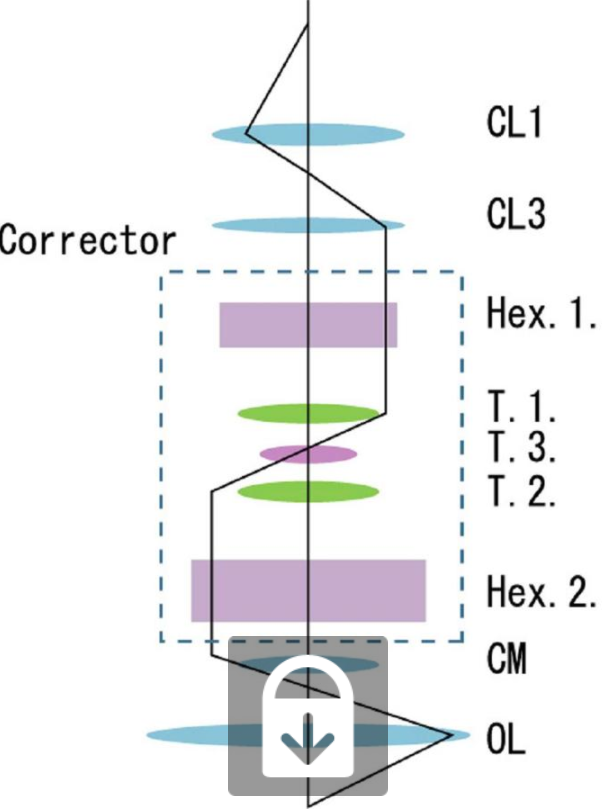
1.1. Aberration Correction
The addition of an aberration corrector to STEMs enables electron probes to be focused to sub-angstrom diameters, allowing images with sub-angstrom resolution to be acquired. This has made it possible to identify individual atomic columns with unprecedented clarity. Aberration-corrected STEM was demonstrated with 1.9 Å resolution in 1997[8] and soon after in 2000 with roughly 1.36 Å resolution.[9] Advanced aberration-corrected STEMs have since been developed with sub-50 pm resolution.[10] Aberration-corrected STEM provides the added resolution and beam current critical to the implementation of atomic resolution chemical and elemental spectroscopic mapping.
2. Applications
Scanning transmission electron microscopes are used to characterize the nanoscale and atomic-scale structure of specimens, providing important insights into the properties and behaviour of materials and biological cells.
2.1. Materials Science
Scanning transmission electron microscopy has been applied to characterize the structure of a wide range of material specimens, including solar cells,[11] semiconductor devices,[12] complex oxides,[13] batteries,[14] fuel cells,[15] catalysts,[16] and 2D materials.[17]
2.2. Biology
The first application of STEM to the imaging of biological molecules was demonstrated in 1971.[18] The advantage of STEM imaging of biological samples is the high contrast of annular dark-field images, which can allow imaging of biological samples without the need for staining. STEM has been widely used to solve a number of structural problems in molecular biology.[19][20][21]
3. STEM Detectors and Imaging Modes
3.1. Annular Dark-Field
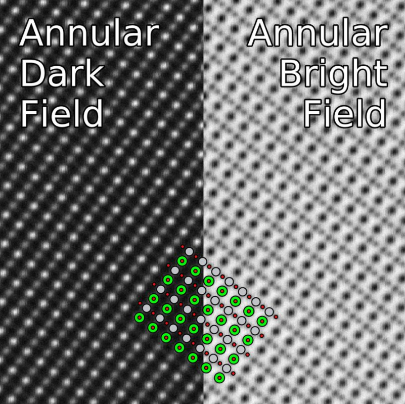
In annular dark-field mode, images are formed by fore-scattered electrons incident on an annular detector, which lies outside of the path of the directly transmitted beam. By using a high-angle ADF detector, it is possible to form atomic resolution images where the contrast of an atomic column is directly related to the atomic number (Z-contrast image).[22] Directly interpretable Z-contrast imaging makes STEM imaging with a high-angle detector an appealing technique in contrast to conventional high-resolution electron microscopy, in which phase-contrast effects mean that atomic resolution images must be compared to simulations to aid interpretation.
3.2. Bright-Field
In STEM, bright-field detectors are located in the path of the transmitted electron beam. Axial bright-field detectors are located in the centre of the cone of illumination of the transmitted beam, and are often used to provide complementary images to those obtained by ADF imaging.[23] Annular bright-field detectors, located within the cone of illumination of the transmitted beam, have been used to obtain atomic resolution images in which the atomic columns of light elements such as oxygen are visible.[24]
3.3. Differential Phase Contrast
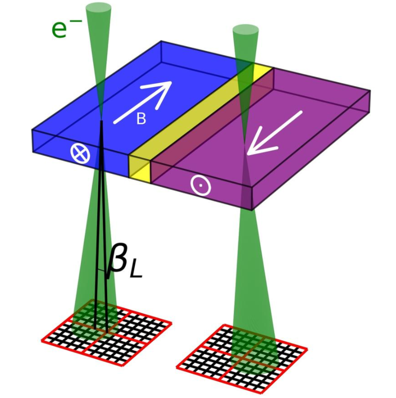
Differential phase contrast (DPC) is an imaging mode which relies on the beam being deflected by electromagnetic fields. In the classical case, the fast electrons in the electron beam is deflected by the Lorentz force, as shown schematically for a magnetic field in the figure to the left. The fast electron with charge −1 e passing through an electric field E and a magnetic field B experiences a force F:
- [math]\displaystyle{ \mathbf{F} = -e\mathbf{E} - e\mathbf{v} \times \mathbf{B} }[/math]
For a magnetic field, this can be expressed as the amount of beam deflection experienced by the electron, βL:[25]
- [math]\displaystyle{ \beta_L = -\frac{e\lambda}{h} \int \mathbf{B} \times d\mathbf{l} }[/math]
where [math]\displaystyle{ \lambda }[/math] is the wavelength of the electron, [math]\displaystyle{ h }[/math] the Planck constant and [math]\displaystyle{ \textstyle\int \mathbf{B} \times d\mathbf{l} }[/math] is integrated magnetic induction along the trajectory of the electron. This last term reduces to [math]\displaystyle{ B_S t }[/math] when the electron beam is perpendicular to a sample of thickness [math]\displaystyle{ t }[/math] with constant in-plane magnetic induction of magnitude [math]\displaystyle{ B_S }[/math]. The beam deflection can then be imaged on a segmented or pixelated detector.[25] This can be used to image magnetic[25][26] and electric fields[27] in materials. While the beam deflection mechanism through the Lorentz force is the most intuitive way of understanding DPC, a quantum mechanical approach is necessary to understand the phase-shift generated by the electromagnetic fields through the Aharonov–Bohm effect.[25]
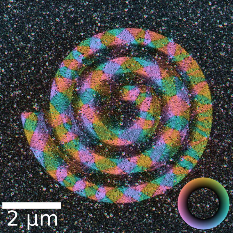
Imaging most ferromagnetic materials require the current in the objective lens of the STEM to be reduced to almost zero. This is due to the sample residing inside the magnetic field of the objective lens, which can be several Tesla, which for most ferromagnetic materials would destroy any magnetic domain structure.[28] However, turning the objective lens almost off drastically increase the amount of aberrations in the STEM probe, leading to an increase in the probe size, and reduction in resolution. By using a probe aberration corrector it is possible to get a resolution of 1 nm.[29]
3.4. Universal Detectors (4D STEM)
Recently, detectors have been developed for STEM that can record a complete convergent-beam electron diffraction pattern of all scattered and unscattered electrons at every pixel in a scan of the sample in a large four-dimensional dataset (a 2D diffraction pattern recorded at every 2D probe position).[30] Due to the four-dimensional nature of the datasets, the term "4D STEM" has become a common name for this technique.[31][32] The 4D datasets generated using the technique can be analyzed to reconstruct images equivalent to those of any conventional detector geometry, and can be used to map fields in the sample at high spatial resolution, including information about strain and electric fields.[33] The technique can also be used to perform ptychography.
4. Spectroscopy in STEM
4.1. Electron Energy Loss Spectroscopy
As the electron beam passes through the sample, some electrons in the beam lose energy via inelastic scattering interactions with electrons in the sample. In electron energy loss spectroscopy (EELS), the energy lost by the electrons in the beam is measured using an electron spectrometer, allowing features such as plasmons, and elemental ionization edges to be identified. Energy resolution in EELS is sufficient to allow the fine structure of ionization edges to be observed, which means that EELS can be used for chemical mapping, as well as elemental mapping.[34] In STEM, EELS can be used to spectroscopically map a sample at atomic resolution.[35] Recently developed monochromators can achieve an energy resolution of ~10 meV in EELS, allowing vibrational spectra to be acquired in STEM.[36]
4.2. Energy-Dispersive X-Ray Spectroscopy
In energy-dispersive X-ray spectroscopy (EDX) or (EDXS), which is also referred to in literature as X-ray energy dispersive spectroscopy (EDS) or (XEDS), an X-ray spectrometer is used to detect the characteristic X-rays that are emitted by atoms in the sample as they are ionized by electron in the beam. In STEM, EDX is typically used for compositional analysis and elemental mapping of samples.[37] Typical X-ray detectors for electron microscopes cover only a small solid angle, which makes X-ray detection relatively inefficient since X-rays are emitted from the sample in every direction. However, detectors covering large solid angles have been recently developed,[38] and atomic resolution X-ray mapping has even been achieved.[39]
5. Convergent-beam Electron Diffraction
Convergent-beam electron diffraction (CBED) is a STEM technique that provides information about crystal structure at a specific point in a sample. In CBED, the width of the area a diffraction pattern is acquired from is equal to the size of the probe used, which can be smaller than 1 Å in an aberration-corrected STEM (see above). CBED differs from conventional electron diffraction in that CBED patterns consist of diffraction disks, rather than spots. The width of CBED disks is determined by the convergence angle of the electron beam. Other features, such as Kikuchi lines are often visible in CBED patterns. CBED can be used to determine the point and space groups of a specimen.[40]
6. Quantitative Scanning Transmission Electron Microscopy (QSTEM)
Electron microscopy has accelerated research in materials science by quantifying properties and features from nanometer-resolution imaging with STEM, which is crucial in observing and confirming factors, such as thin film deposition, crystal growth, surface structure formation, and dislocation movement. Until recently, most papers have inferred the properties and behaviors of material systems based on these images without being able to establish rigorous rules for what exactly is observed. The techniques that have emerged as a result of interest in quantitative scanning transmission electron microscopy (QSTEM) closes this gap by allowing researchers to identify and quantify structural features that are only visible using high-resolution imaging in a STEM. Widely available image processing techniques are applied to high-angle annular dark field (HAADF) images of atomic columns to precisely locate their positions and the material's lattice constant(s). This ideology has been successfully used to quantify structural properties, such as strain and bond angle, at interfaces and defect complexes. QSTEM allows researchers to now compare the experimental data to theoretical simulations both qualitatively and quantitatively. Recent studies published have shown that QSTEM can measure structural properties, such as interatomic distances, lattice distortions from point defects, and locations of defects within an atomic column, with high accuracy. QSTEM can also be applied to selected area diffraction patterns and convergent beam diffraction patterns to quantify the degree and types of symmetry present in a specimen. Since any materials research requires structure-property relationship studies, this technique is applicable to countless fields. A notable study is the mapping of atomic column intensities and interatomic bond angles in a mott-insulator system.[41] This was the first study to show that the transition from the insulating to conducting state was due to a slight global decrease in distortion, which was concluded by mapping the interatomic bond angles as a function of the dopant concentration. This effect is not visible by the human eye in a standard atomic-scale image enabled by HAADF imaging, thus this important finding was only made possible due to the application of QSTEM.
QSTEM analysis can be achieved using commonplace software and programming languages, such as MatLab or Python, with the help of toolboxes and plug-ins that serve to expedite the process. This is analysis that can be performed virtually anywhere. Consequently, the largest roadblock is acquiring a high-resolution, aberration-corrected scanning transmission electron microscope that can provide the images necessary to provide accurate quantification of structural properties at the atomic level. Most university research groups, for example, require permission to use such high-end electron microscopes at national lab facilities, which requires excessive time commitment. Universal challenges mainly involve becoming accustomed to the programming language desired and writing software that can tackle the very specific problems for a given material system. For example, one can imagine how a different analysis technique, and thus a separate image processing algorithm, is necessary for studying ideal cubic versus complex monoclinic structures.
7. Other STEM Techniques
Specialized sample holders or modifications to the microscope can allow a number of additional techniques to be performed in STEM. Some examples are described below.
7.1. STEM Tomography
STEM tomography allows the complete three-dimensional internal and external structure of a specimen to be reconstructed from a tilt-series of 2D projection images of the specimen acquired at incremental tilts.[42] High angle ADF STEM is a particularly useful imaging mode for electron tomography because the intensity of high angle ADF-STEM images varies only with the projected mass-thickness of the sample, and the atomic number of atoms in the sample. This yields highly interpretable three dimensional reconstructions.[43]
7.2. Cryo-STEM
Cryogenic electron microscopy in STEM (Cryo-STEM) allows specimens to be held in the microscope at liquid nitrogen or liquid helium temperatures. This is useful for imaging specimens that would be volatile in high vacuum at room temperature. Cryo-STEM has been used to study vitrified biological samples,[44] vitrified solid-liquid interfaces in material specimens,[45] and specimens containing elemental sulfur, which is prone to sublimation in electron microscopes at room temperature.[46]
7.3. In Situ/Environmental STEM
In order to study the reactions of particles in gaseous environments, a STEM may be modified with a differentially pumped sample chamber to allow gas flow around the sample, whilst a specialized holder is used to control the reaction temperature.[47] Alternatively a holder mounted with an enclosed gas flow cell may be used.[48] Nanoparticles and biological cells have been studied in liquid environments using liquid-phase electron microscopy[49] in STEM, accomplished by mounting a microfluidic enclosure in the specimen holder.[50][51][52]
7.4. Low-Voltage STEM
A low-voltage electron microscope (LVEM) is an electron microscope that is designed to operate at relatively low electron accelerating voltages of between 0.5 and 30 kV. Some LVEMs can function as an SEM, a TEM, and a STEM in a single compact instrument. Using a low beam voltage increases image contrast which is especially important for biological specimens. This increase in contrast significantly reduces, or even eliminates the need to stain biological samples. Resolutions of a few nm are possible in TEM, SEM and STEM modes. The low energy of the electron beam means that permanent magnets can be used as lenses and thus a miniature column that does not require cooling can be used.[53][54]
The content is sourced from: https://handwiki.org/wiki/Engineering:Scanning_transmission_electron_microscopy
References
- de Broglie (1925). "Recherches sur la Theorie des Quanta". Annales de Physique 10 (3): 22–128. doi:10.1051/anphys/192510030022. Bibcode: 1925AnPh...10...22D. https://tel.archives-ouvertes.fr/tel-00006807/document. translation
- von Ardenne, M (1938). "Das Elektronen-Rastermikroskop. Theoretische Grundlagen". Z. Phys. 109 (9–10): 553–572. doi:10.1007/BF01341584. Bibcode: 1938ZPhy..109..553V. https://dx.doi.org/10.1007%2FBF01341584
- von Ardenne, M (1938). "Das Elektronen-Rastermikroskop. Praktische Ausführung". Z. Tech. Phys. 19: 407–416.
- D. McMullan, SEM 1928 – 1965 http://www-g.eng.cam.ac.uk/125/achievements/mcmullan/mcm.htm
- Crewe, Albert V; Isaacson, M.; Johnson, D. (1969). "A Simple Scanning Electron Microscope". Rev. Sci. Instrum. 40 (2): 241–246. doi:10.1063/1.1683910. Bibcode: 1969RScI...40..241C. https://digital.library.unt.edu/ark:/67531/metadc1061663/.
- Crewe, Albert V; Wall, J.; Langmore, J. (1970). "Visibility of a single atom". Science 168 (3937): 1338–1340. doi:10.1126/science.168.3937.1338. PMID 17731040. Bibcode: 1970Sci...168.1338C. https://dx.doi.org/10.1126%2Fscience.168.3937.1338
- Shin, D.H.; Kirkland, E.J.; Silcox, J. (1989). "Annular dark field electron microscope images with better than 2 Å resolution at 100 kV". Appl. Phys. Lett. 55 (23): 2456. doi:10.1063/1.102297. Bibcode: 1989ApPhL..55.2456S. https://dx.doi.org/10.1063%2F1.102297
- Batson, P.E.; Domenincucci, A.G.; Lemoine, E. (1997). "Atomic resolution electronic structure in device development". Microsc. Microanal. 3 (S2): 645. doi:10.1017/S1431927600026064. Bibcode: 1997MiMic...3S.645B. https://dx.doi.org/10.1017%2FS1431927600026064
- Dellby, N.; Krivanek, O. L.; Nellist, P. D.; Batson, P. E.; Lupini, A. R. (2001). "Progress in aberration-corrected scanning transmission electron microscopy". Microscopy 50 (3): 177–185. doi:10.1093/jmicro/50.3.177. PMID 11469406. https://dx.doi.org/10.1093%2Fjmicro%2F50.3.177
- Kisielowski, C.; Freitag, B.; Bischoff, M.; Van Lin, H.; Lazar, S.; Knippels, G.; Tiemeijer, P.; Van Der Stam, M. et al. (2008). "Detection of Single Atoms and Buried Defects in Three Dimensions by Aberration-Corrected Electron Microscope with 0.5-Å Information Limit". Microscopy and Microanalysis 14 (5): 469–477. doi:10.1017/S1431927608080902. PMID 18793491. Bibcode: 2008MiMic..14..469K. https://semanticscholar.org/paper/0cb75075e81b1653a6dfe24af122a5fce9e112c6.
- Kosasih, Felix Utama; Ducati, Caterina (May 2018). "Characterising degradation of perovskite solar cells through in-situ and operando electron microscopy". Nano Energy 47: 243–256. doi:10.1016/j.nanoen.2018.02.055. https://www.repository.cam.ac.uk/handle/1810/275845.
- Van Benthem, Klaus; Lupini, Andrew R.; Kim, Miyoung; Baik, Hion Suck; Doh, Seokjoo; Lee, Jong-Ho; Oxley, Mark P.; Findlay, Scott D. et al. (2005). "Three-dimensional imaging of individual hafnium atoms inside a semiconductor device". Applied Physics Letters 87 (3): 034104. doi:10.1063/1.1991989. Bibcode: 2005ApPhL..87c4104V. https://semanticscholar.org/paper/8d539d3da2212626c1dd3decfb61d899ecd5528a.
- Reyren, N.; Thiel, S.; Caviglia, A. D.; Kourkoutis, L. F.; Hammerl, G.; Richter, C.; Schneider, C. W.; Kopp, T. et al. (2007). "Superconducting Interfaces Between Insulating Oxides". Science 317 (5842): 1196–1199. doi:10.1126/science.1146006. PMID 17673621. Bibcode: 2007Sci...317.1196R. https://hal.archives-ouvertes.fr/hal-02076434/file/reyren%20July%2018%2C%2017%2000.pdf.
- Lin, Feng; Markus, Isaac M.; Nordlund, Dennis; Weng, Tsu-Chien; Asta, Mark D.; Xin, Huolin L.; Doeff, Marca M. (2014). "Surface reconstruction and chemical evolution of stoichiometric layered cathode materials for lithium-ion batteries". Nature Materials 5: 1196–1199. doi:10.1038/ncomms4529. PMID 24670975. Bibcode: 2014NatCo...5.3529L. https://www.researchgate.net/publication/261138095.
- Xin, Huolin L.; Mundy, Julia A.; Liu, Zhongyi; Cabezas, Randi; Hovden, Robert; Kourkoutis, Lena Fitting; Zhang, Junliang; Subramanian, Nalini P. et al. (2012). "Atomic-Resolution Spectroscopic Imaging of Ensembles of Nanocatalyst Particles Across the Life of a Fuel Cell". Nano Letters 12 (1): 490–497. doi:10.1021/nl203975u. PMID 22122715. Bibcode: 2012NanoL..12..490X. https://dx.doi.org/10.1021%2Fnl203975u
- Jones, Lewys; MacArthur, Katherine E.; Fauske, Vidar T.; Van Helvoort, Antonius T. J.; Nellist, Peter D. (2014). "Rapid Estimation of Catalyst Nanoparticle Morphology and Atomic-Coordination by High-Resolution Z-Contrast Electron Microscopy". Nano Letters 14 (11): 6336–6341. doi:10.1021/nl502762m. PMID 25340541. Bibcode: 2014NanoL..14.6336J. https://dx.doi.org/10.1021%2Fnl502762m
- Huang, P. Y.; Kurasch, S.; Alden, J. S.; Shekhawat, A.; Alemi, A. A.; McEuen, P. L.; Sethna, J. P.; Kaiser, U. et al. (2013). "Imaging Atomic Rearrangements in Two-Dimensional Silica Glass: Watching Silica's Dance". Science 342 (6155): 224–227. doi:10.1126/science.1242248. PMID 24115436. Bibcode: 2013Sci...342..224H. https://semanticscholar.org/paper/25f3113162758a01548ef7200de1024dad872c3a.
- Wall, J.S. (1971) A high resolution scanning electron microscope for the study of single biological molecules. PhD thesis, University of Chicago
- Wall JS; Hainfeld JF (1986). "Mass mapping with the scanning transmission electron microscope". Annu Rev Biophys Biophys Chem 15: 355–76. doi:10.1146/annurev.bb.15.060186.002035. PMID 3521658. https://dx.doi.org/10.1146%2Fannurev.bb.15.060186.002035
- Hainfeld JF; Wall JS (1988). "High resolution electron microscopy for structure and mapping". Biotechnology and the Human Genome. Basic Life Sciences. 46. Boston, MA. 131–47. doi:10.1007/978-1-4684-5547-2_13. ISBN 978-1-4684-5549-6. https://dx.doi.org/10.1007%2F978-1-4684-5547-2_13
- Wall JS, Simon MN (2001). "Scanning transmission electron microscopy of DNA-protein complexes". DNA-Protein Interactions. Methods Mol Biol. 148. pp. 589–601. doi:10.1385/1-59259-208-2:589. ISBN 978-1-59259-208-1. https://dx.doi.org/10.1385%2F1-59259-208-2%3A589
- Pennycook, S.J.; Jesson, D.E. (1991). "High-resolution Z-contrast imaging of crystals". Ultramicroscopy 37 (1–4): 14–38. doi:10.1016/0304-3991(91)90004-P. https://zenodo.org/record/1258469.
- Xu, Peirong; Kirkland, Earl J.; Silcox, John; Keyse, Robert (1990). "High-resolution imaging of silicon (111) using a 100 keV STEM". Ultramicroscopy 32 (2): 93–102. doi:10.1016/0304-3991(90)90027-J. https://dx.doi.org/10.1016%2F0304-3991%2890%2990027-J
- Findlay, S.D.; Shibata, N.; Sawada, H.; Okunishi, E.; Kondo, Y.; Ikuhara, Y. (2010). "Dynamics of annular bright field imaging in scanning transmission electron microscopy". Ultramicroscopy 32 (7): 903–923. doi:10.1016/j.ultramic.2010.04.004. PMID 20434265. https://dx.doi.org/10.1016%2Fj.ultramic.2010.04.004
- Krajnak, Matus; McGrouther, Damien; Maneuski, Dzmitry; Shea, Val O'; McVitie, Stephen (June 2016). "Pixelated detectors and improved efficiency for magnetic imaging in STEM differential phase contrast". Ultramicroscopy 165: 42–50. doi:10.1016/j.ultramic.2016.03.006. PMID 27085170. https://dx.doi.org/10.1016%2Fj.ultramic.2016.03.006
- McVitie, S.; Hughes, S.; Fallon, K.; McFadzean, S.; McGrouther, D.; Krajnak, M.; Legrand, W.; Maccariello, D. et al. (9 April 2018). "A transmission electron microscope study of Néel skyrmion magnetic textures in multilayer thin film systems with large interfacial chiral interaction". Scientific Reports 8 (1): 5703. doi:10.1038/s41598-018-23799-0. PMID 29632330. Bibcode: 2018NatSR...8.5703M. http://www.pubmedcentral.nih.gov/articlerender.fcgi?tool=pmcentrez&artid=5890272
- Haas, Benedikt; Rouvière, Jean-Luc; Boureau, Victor; Berthier, Remy; Cooper, David (March 2019). "Direct comparison of off-axis holography and differential phase contrast for the mapping of electric fields in semiconductors by transmission electron microscopy.". Ultramicroscopy 198: 58–72. doi:10.1016/j.ultramic.2018.12.003. PMID 30660032. https://dx.doi.org/10.1016%2Fj.ultramic.2018.12.003
- Chapman, J N (14 April 1984). "The investigation of magnetic domain structures in thin foils by electron microscopy". Journal of Physics D: Applied Physics 17 (4): 623–647. doi:10.1088/0022-3727/17/4/003. https://dx.doi.org/10.1088%2F0022-3727%2F17%2F4%2F003
- McVitie, S.; McGrouther, D.; McFadzean, S.; MacLaren, D.A.; O’Shea, K.J.; Benitez, M.J. (May 2015). "Aberration corrected Lorentz scanning transmission electron microscopy". Ultramicroscopy 152: 57–62. doi:10.1016/j.ultramic.2015.01.003. PMID 25677688. http://eprints.gla.ac.uk/102200/2/102200.pdf.
- Tate, Mark W.; Purohit, Prafull; Chamberlain, Darol; Nguyen, Kayla X.; Hovden, Robert; Chang, Celesta S.; Deb, Pratiti; Turgut, Emrah et al. (2016). "High Dynamic Range Pixel Array Detector for Scanning Transmission Electron Microscopy". Microscopy and Microanalysis 22 (1): 237–249. doi:10.1017/S1431927615015664. PMID 26750260. Bibcode: 2016MiMic..22..237T. https://dx.doi.org/10.1017%2FS1431927615015664
- Ophus, Colin (June 2019). "Four-Dimensional Scanning Transmission Electron Microscopy (4D-STEM): From Scanning Nanodiffraction to Ptychography and Beyond" (in en). Microscopy and Microanalysis 25 (3): 563–582. doi:10.1017/S1431927619000497. ISSN 1431-9276. PMID 31084643. Bibcode: 2019MiMic..25..563O. https://dx.doi.org/10.1017%2FS1431927619000497
- (in en) 4D STEM with a direct electron detector. doi:10.1002/was.00010003. https://analyticalscience.wiley.com/do/10.1002/was.00010003. Retrieved 2020-02-11.
- Ciston, Jim; Ophus, Colin; Ercius, Peter; Yang, Hao; Dos Reis, Roberto; Nelson, Christopher T.; Hsu, Shang-Lin; Gammer, Christoph et al. (2016). "Multimodal Acquisition of Properties and Structure with Transmission Electron Reciprocal-space (MAPSTER) Microscopy". Microscopy and Microanalysis 22(S3) (S3): 1412–1413. doi:10.1017/S143192761600790X. Bibcode: 2016MiMic..22S1412C. https://dx.doi.org/10.1017%2FS143192761600790X
- Egerton,R.F., ed (2011). Electron Energy-Loss Spectroscopy in the Electron Microscope. Springer. ISBN 978-1-4419-9582-7.
- Mundy, Julia A.; Hikita, Yasuyuki; Hidaka, Takeaki; Yajima, Takeaki; Higuchi, Takuya; Hwang, Harold Y.; Muller, David A.; Kourkoutis, Lena F. (2014). "Visualizing the interfacial evolution from charge compensation to metallic screening across the manganite metal–insulator transition". Nature Communications 5: 3464. doi:10.1038/ncomms4464. PMID 24632721. Bibcode: 2014NatCo...5.3464M. https://dx.doi.org/10.1038%2Fncomms4464
- Krivanek, Ondrej L.; Lovejoy, Tracy C.; Dellby, Niklas; Aoki, Toshihiro; Carpenter, R. W.; Rez, Peter; Soignard, Emmanuel; Zhu, Jiangtao et al. (2016). "Vibrational spectroscopy in the electron microscope". Nature 514 (7521): 209–212. doi:10.1038/nature13870. PMID 25297434. Bibcode: 2014Natur.514..209K. https://dx.doi.org/10.1038%2Fnature13870
- Friel, J.J.; Lyman, C.E. (2006). "Tutorial Review: X-ray Mapping in Electron-Beam Instruments". Microscopy and Microanalysis 12 (1): 2–25. doi:10.1017/S1431927606060211. PMID 17481338. Bibcode: 2006MiMic..12....2F. https://dx.doi.org/10.1017%2FS1431927606060211
- Zaluzec, Nestor J. (2009). "Innovative Instrumentation for Analysis of Nanoparticles: The π Steradian Detector". Microsc. Today 17 (4): 56–59. doi:10.1017/S1551929509000224. https://semanticscholar.org/paper/840ee2ed0dd54c352d40fadae6ddf7ac164b567f.
- Chen, Z.; Weyland, M.; Sang, X.; Xu, W.; Dycus, J.H.; Lebeau, J.M.; d'Alfonso, A.J.; Allen, L.J. et al. (2016). "Quantitative atomic resolution elemental mapping via absolute-scale energy dispersive X-ray spectroscopy". Ultramicroscopy 168 (4): 7–16. doi:10.1016/j.ultramic.2016.05.008. PMID 27258645. https://dx.doi.org/10.1016%2Fj.ultramic.2016.05.008
- null
- Kim, Honggyu; Marshall, Patrick B.; Ahadi, Kaveh; Mates, Thomas E.; Mikheev, Evgeny; Stemmer, Susanne (2017). "Response of the Lattice across the Filling-Controlled Mott Metal-Insulator Transition of a Rare Earth Titanate". Physical Review Letters 119 (18): 186803. doi:10.1103/PhysRevLett.119.186803. PMID 29219551. Bibcode: 2017PhRvL.119r6803K. https://dx.doi.org/10.1103%2FPhysRevLett.119.186803
- Levin, Barnaby D.A.; Padgett, Elliot; Chen, Chien-Chun; Scott, M.C.; Xu, Rui; Theis, Wolfgang; Jiang, Yi; Yang, Yongsoo et al. (2016). "Nanomaterial datasets to advance tomography in scanning transmission electron microscopy". Scientific Data 3 (160041): 160041. doi:10.1038/sdata.2016.41. PMID 27272459. Bibcode: 2016NatSD...360041L. http://www.pubmedcentral.nih.gov/articlerender.fcgi?tool=pmcentrez&artid=4896123
- Midgley, P. A.; Weyland, M. (2003). "3D electron microscopy in the physical sciences: The development of Z-contrast and EFTEM tomography". Ultramicroscopy 96 (3–4): 413–431. doi:10.1016/S0304-3991(03)00105-0. PMID 12871805. https://dx.doi.org/10.1016%2FS0304-3991%2803%2900105-0
- Wolf, Sharon Grayer; Houben, Lothar; Elbaum, Michael (2014). "Cryo-scanning transmission electron tomography of vitrified cells". Nature Methods 11 (4): 423–428. doi:10.1038/nmeth.2842. PMID 24531421. https://dx.doi.org/10.1038%2Fnmeth.2842
- Zachman, Michael J.; Asenath-Smith, Emily; Estroff, Lara A.; Kourkoutis, Lena F. (2016). "Site-Specific Preparation of Intact Solid–Liquid Interfaces by Label-Free In Situ Localization and Cryo-Focused Ion Beam Lift-Out". Microscopy and Microanalysis 22 (6): 1338–1349. doi:10.1017/S1431927616011892. PMID 27869059. Bibcode: 2016MiMic..22.1338Z. https://dx.doi.org/10.1017%2FS1431927616011892
- Levin, Barnaby D.A.; Zachman, Michael J.; Werner, Jörg G.; Sahore, Ritu; Nguyen, Kayla X.; Han, Yimo; Xie, Baoquan; Ma, Lin et al. (2017). "Characterization of Sulfur and Nanostructured Sulfur Battery Cathodes in Electron Microscopy Without Sublimation Artifacts". Microscopy and Microanalysis 23 (1): 155–162. doi:10.1017/S1431927617000058. PMID 28228169. Bibcode: 2017MiMic..23..155L. https://zenodo.org/record/889883.
- Boyes, Edward D.; Ward, Michael R.; Lari, Leonardo; Gai, Pratibha L. (2013). "ESTEM imaging of single atoms under controlled temperature and gas environment conditions in catalyst reaction studies". Annalen der Physik 525 (6): 423–429. doi:10.1002/andp.201300068. Bibcode: 2013AnP...525..423B. https://dx.doi.org/10.1002%2Fandp.201300068
- Li, Y.; Zakharov, D.; Zhao, S.; Tappero, R.; Jung, U.; Elsen, A.; Baumann, Ph.; Nuzzo, R.G. et al. (2015). "Complex structural dynamics of nanocatalysts revealed in Operando conditions by correlated imaging and spectroscopy probes". Nature Communications 6: 7583. doi:10.1038/ncomms8583. PMID 26119246. Bibcode: 2015NatCo...6.7583L. http://www.pubmedcentral.nih.gov/articlerender.fcgi?tool=pmcentrez&artid=4491830
- de Jonge, N.; Ross, F.M. (2011). "Electron microscopy of specimens in liquid". Nature Nanotechnology 6 (8): 695–704. doi:10.1038/nmat944. PMID 12872162. Bibcode: 2003NatMa...2..532W. https://www.researchgate.net/publication/51735636.
- de Jonge, N.; Peckys, D.B.; Kremers, G.J.; Piston, D.W. (2009). "Electron microscopy of whole cells in liquid with nanometer resolution". Proceedings of the National Academy of Sciences of the USA 106 (7): 2159–2164. doi:10.1073/pnas.0809567106. PMID 19164524. Bibcode: 2009PNAS..106.2159J. http://www.pubmedcentral.nih.gov/articlerender.fcgi?tool=pmcentrez&artid=2650183
- Ievlev, Anton V.; Jesse, Stephen; Cochell, Thomas J.; Unocic, Raymond R.; Protopopescu, Vladimir A.; Kalinin, Sergei V. (2015). "Quantitative Description of Crystal Nucleation and Growth from in Situ Liquid Scanning Transmission Electron Microscopy". ACS Nano 9 (12): 11784–11791. doi:10.1021/acsnano.5b03720. PMID 26509714. https://dx.doi.org/10.1021%2Facsnano.5b03720
- Unocic, Raymond R.; Lupini, Andrew R.; Borisevich, Albina Y.; Cullen, David A.; Kalinin, Sergei V.; Jesse, Stephen (2016). "Direct-write liquid phase transformations with a scanning transmission electron microscope". Nanoscale 8 (34): 15581–15588. doi:10.1039/C6NR04994J. PMID 27510435. https://dx.doi.org/10.1039%2FC6NR04994J
- Nebesářová, Jana; Vancová, Marie (2007). "How to Observe Small Biological Objects in Low-Voltage Electron Microscope". Microscopy and Microanalysis 13 (S03): 248–249. doi:10.1017/S143192760708124X. Bibcode: 2007MiMic..13S.248N. https://www.cambridge.org/core/journals/microscopy-and-microanalysis/article/div-classtitlehow-to-observe-small-biological-objects-in-low-voltage-electron-microscopediv/9A089B9CA06B9F5D18A2CD12EA4B2A24.
- Drummy, Lawrence, F.; Yang, Junyan; Martin, David C. (2004). "Low-voltage electron microscopy of polymer and organic molecular thin films". Ultramicroscopy 99 (4): 247–256. doi:10.1016/j.ultramic.2004.01.011. PMID 15149719. https://dx.doi.org/10.1016%2Fj.ultramic.2004.01.011