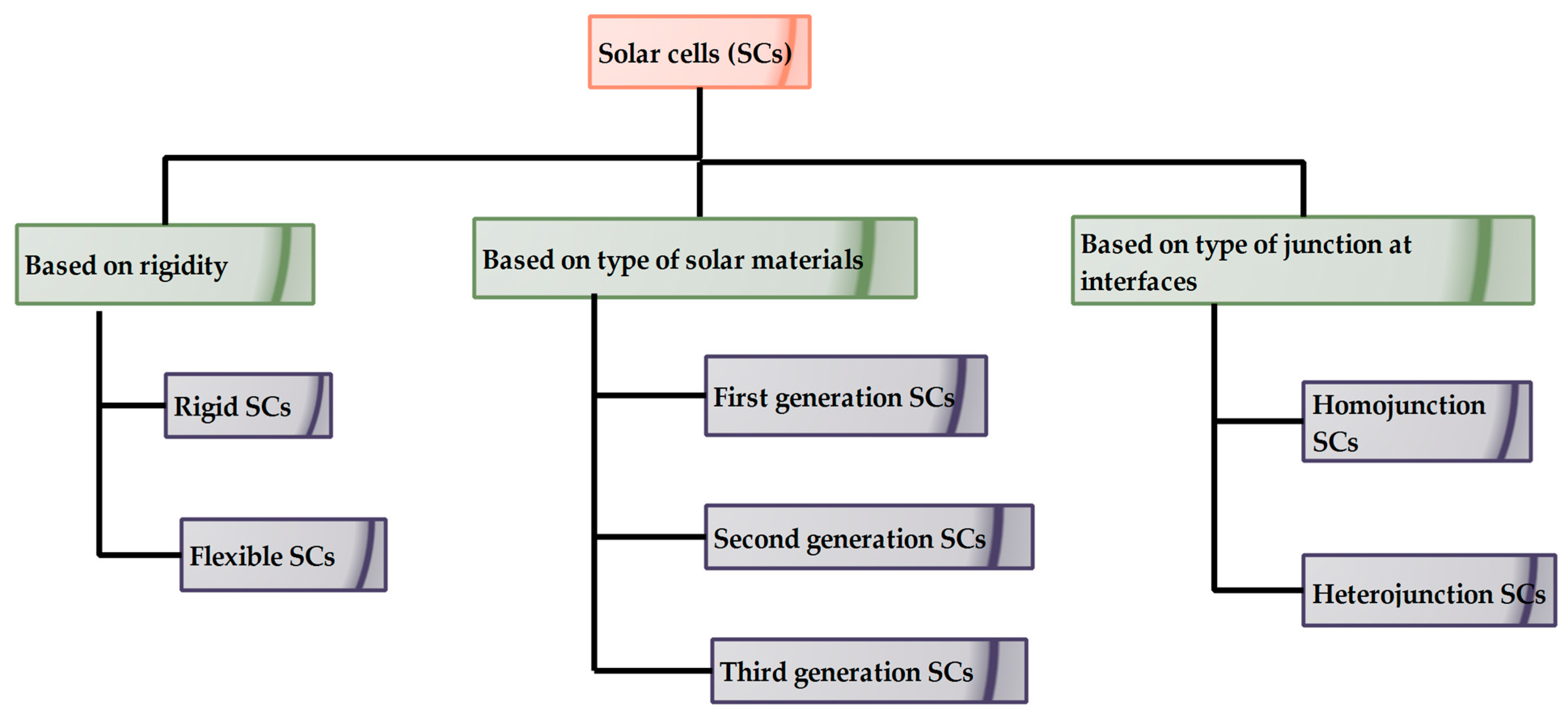
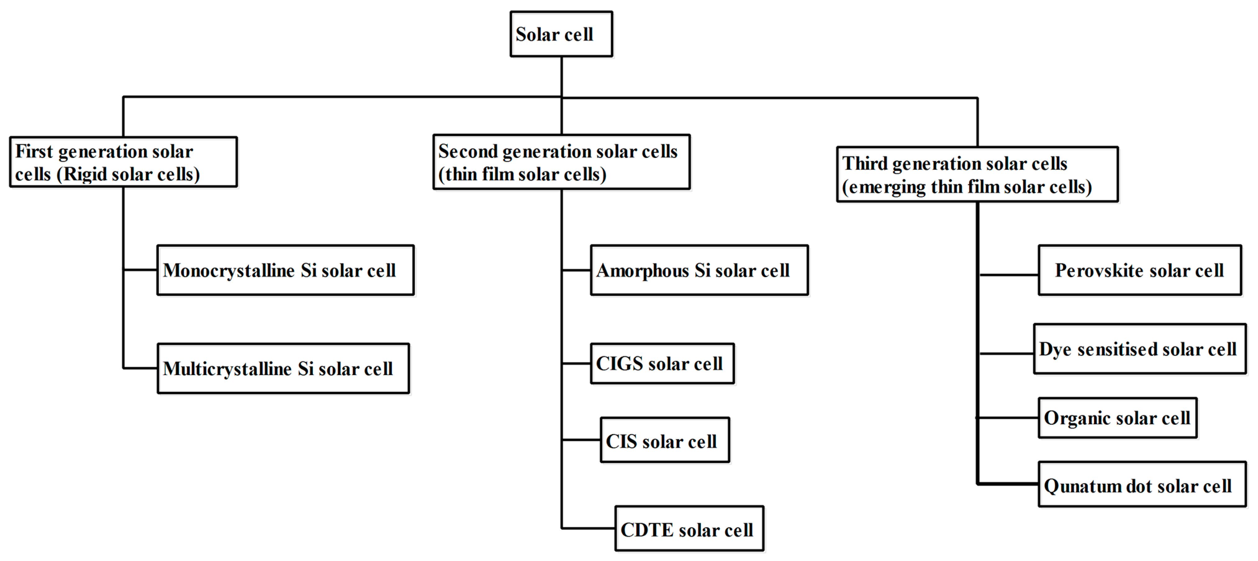
Due to the surge in silicon demand for solar modules, thin-film photovoltaic (PV) modules have a potential to penetrate the market in significant numbers. As an alternate candidate, thin film technologies in PVs have the ability to achieve better performance. The competing thin-film PV technologies have the flexibility to adapt to any sort of curvature compared to rigid solar cells (SCs). Due to the peculiar characteristics of newer solar materials, stability issues, reflection losses, advancements in electrode materials and dopant materials with a photoactive layer are current challenges driving the industrial-academic voyage of development of solar materials for the betterment of Photo-conversion Efficiency (PCE). Based on the photoactive materials used over time, SC evolution was broadly classified into first, second and third generation SCs.
- solar cells
- photo-absorber materials
- working mechanism
- thin film solar cells
1. Introduction
2. Second Generation Solar Cells
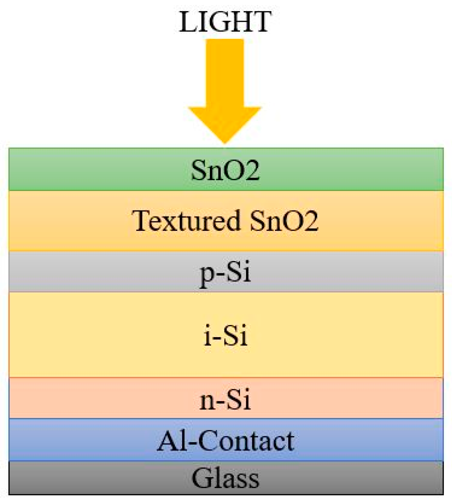
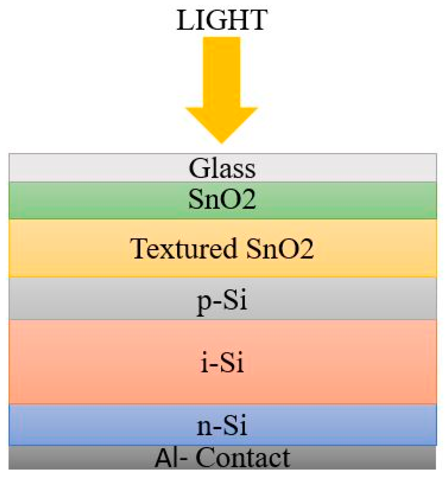
2.1. Amorphous Silicon Solar Cells
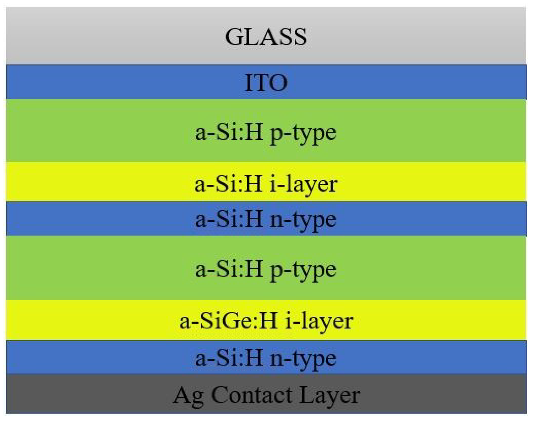
-
Simple working mechanism and inexpensive
-
With optimal thickness, light absorption is higher than in the C-Si
-
Lesser raw material is required
-
The capability to adhere over any sort of surfaces.
-
Lesser working life due to low hole-mobility
-
Harmful gases were needed during fabrication process [33]
-
Mostly absorbs light at a wavelength not greater than 700 nm.
| S.No | Absorber Material | Voc (V) |
Jsc (mA/cm2) |
FF | eff | Ref |
|---|---|---|---|---|---|---|
| 1 | μc-Si:H | 0.542 | 27.44 | 73.8 | 10.97 | [31] |
| 2 | μc-Si:H | 1.411 | 12.6 | 67.8 | 12.1 | [34] |
| 3 | a-Si n type | 0.704 | 42.4 | 82.6 | 24.7 | [35] |
| 4 | a-Si:H | 0.877 | 17.28 | 66.6 | 10.09 | [36] |
| 5 | μc-Si:H | 0.548 | 29.39 | 73.1 | 11.77 | [37] |
| 6 | a-Si:H | 0.896 | 16.36 | 69.8 | 10.22 | [37] |
| 7 | μc-Si:H | 1.322 | 13.02 | 69 | 11.9 | [38] |
| 8 | a-Si:H μc-Si:H μc-Si:H | 1.936 | 8.96 | 71.5 | 12.41 | [39] |
| 9 | μc-Si:H | 0.521 | 28.17 | 71.6 | 10.5 | [40] |
| 10 | a-Si:H μc-Si:H μc-Si:H | 1.901 | 9.92 | 72.1 | 13.46 | [41] |
2.2. CIGS Solar Cell
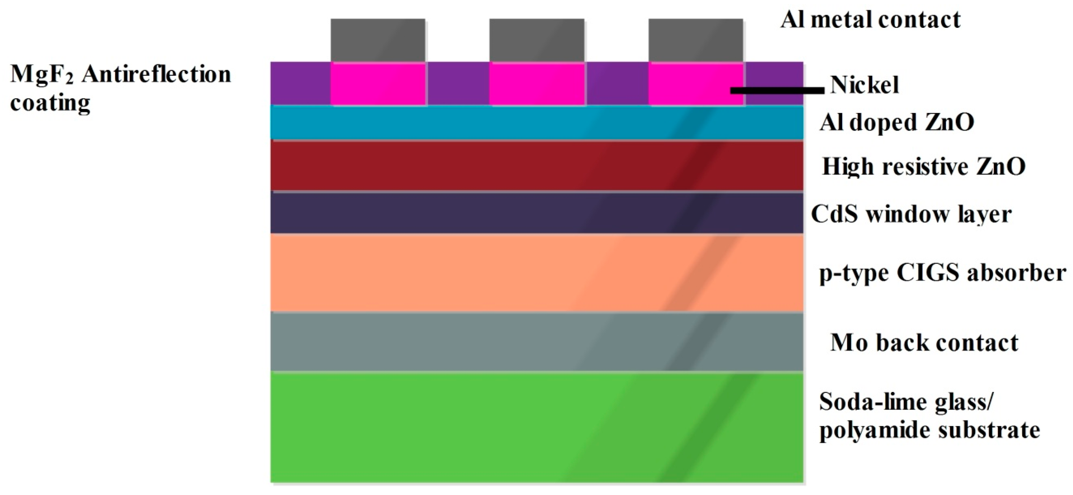
| S.No | Cell Architecture | Inference | Voc (V) | Jsc (mA cm−2) |
FF (%) |
Eff (%) |
Ref |
|---|---|---|---|---|---|---|---|
| 1. | Mo-N back contact diffusion barrier deposition in CIGS SC | 0.622 | 28.67 | 67.53 | 12.05 | [57] | |
| 2. | alkali post deposition treatment of RbF | 0.741 | 37.8 | 80.6 | 22.66 | [58] | |
| 3. | glass/Mo/CIGS/CdS/i-ZnO/TCO/Au | CdS buffer layer deposition through chemical bath method, effect of i-ZnO high resistive layer | 0.661 | 32.08 | 78.9 | 15.50 | [59] |
| 4. | high mobility TCO with 1 eV absorbers | 0.609 | 42.3 | 74.6 | 19.20 | [60] | |
| 5. | Mo/Si/CIGS/ZnS/ZnO | impact of silicon inclusion to reduce the cell thickness and influence of thickness and gallium concentration of the CIGS absorber layer on the performance | 0.6903 | 37.57 | 81.03 | 21.08 | [61] |
| 6. | ZnO NWs/AZO/ZnS/CIGS/Mo/Thermal electric generator | enhanced performance achieved by ZnO NWs with CIGS SC along with series connection of Thermal electric generator | 0.85 | 38.55 | 67.2 | 22.02 | [62] |
| 7. | (Ni/Al)/MgF2/Al:ZnO/CdS/(KF-PDT/CIGS)/Mo/SLG | influence of light-soaking, heat-soaking, and combined LS and HS on KF-treated and KF-free CIGS SCs with CBD-CdS buffer layer | [63] | ||||
| 8. | ZnO/Buffer n-ZnS/p-CIGS/Mo | effect of ZnS buffer layer | 0.804 | 35.66 | 82.14 | 23.54 | [64] |
| 9. | Al2O3/MgF2)/AZO/i-ZnO/CdS/CIGS/Mo | effect of thickness of ARC over CIGS cell | 31.22 | [65] | |||
| 10. | (Al/Ni)/TCO/CdS/GaOx/CIGS/Mo/Soda-lime glass | gallium oxide deposited by plasma-enhanced atomic layer deposition, as a surface passivation material at the interface of CdS buffer layer of CIGS SC | 0.056 | 1 | 8.22 | 2.60 | [66] |
| 11. | (glass/stainless steel)/Mo/CIGS/CdS/ZnO NWs/ITO | ZnO NWS incorporated in CIGS and the effect of externally applied stress (rigid) and strain (flexible) | 11.40 (stress) 5.96 (strain) | [67] |
-
They are more resistant to heat than Si SCs.
-
The active material (CIGS) does not contain harmful components.
-
Holds easily tunable bandgap, facilitating tandem architecture.
-
Its grain boundaries acts as buffer layer, which inhibits the surface recombination.
-
Achieving improved performance takes longer than Si SCs.
-
Less efficient than conventional SCs.
2.3. CdTe Solar Cell
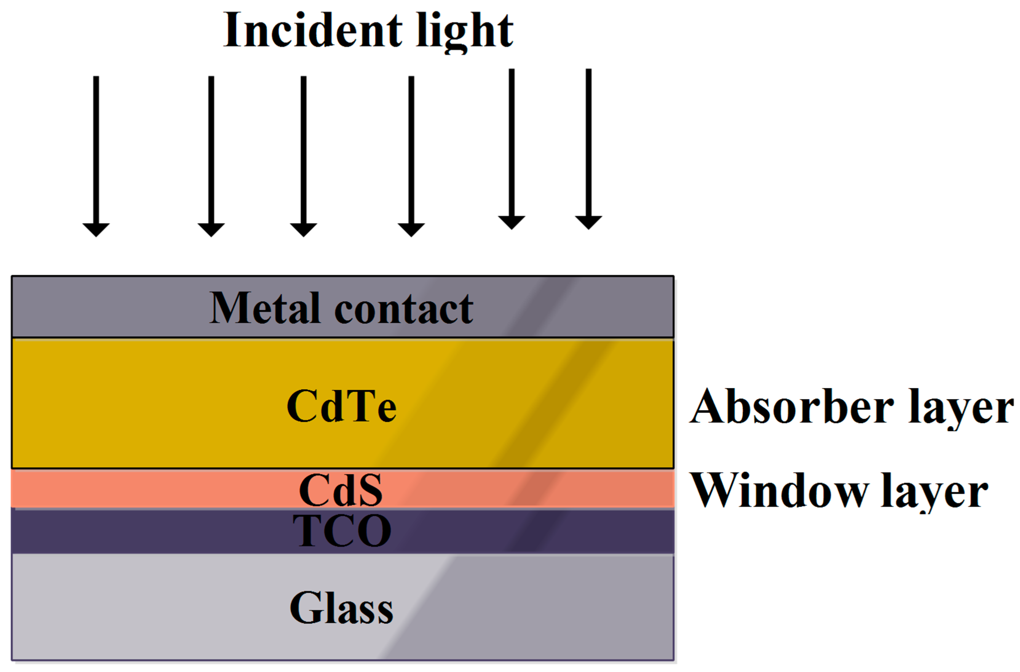
| S.no | Cell Architecture | Voc (mV) | Jsc (mAcm−2) | FF | η (%) | Ref. |
|---|---|---|---|---|---|---|
| 1. | Glass/FTO/n-CdS/n-CdTe/p-CdTe/Au | 730 | 33.8 | 0.62 | 15.30 | [83] |
| 2. | Glass/FTO/CdS/CdTe | 838 | 25 | 0.72 | 15.20 | [84] |
| 3. | glass/FTO/CdS/CdSe/CdTe/ZnTe:Cu/Au | 791 | 27.4 | 13.47 | [85] | |
| 4 | 861 | 26.9 | 0.754 | 17.50 | [71] | |
| 5. | 863 | 28.6 | 0.781 | 19.25 | [86] | |
| 6. | Glass/ZnO:Al/n-CdS/p-CdTe/ZnTe | 1528.5 | 28.355 | 0.497 | 21.57 | [87] |
| 7. | Glass/n-FTO/n-Cd(S,O)/p-CdTe/p-CuZnTe/Au | 848 | 26.6 | 0.733 | 16.60 | [88] |
| 8. | ZnO/CdS/CdTe (0.25/0.05/2.5 micrometers) | 859 | 28.4 | 0.737 | 17.66 | [89] |
| 9. | Quartz/Ti/SiO2/CdTe/ITO | 40.36 | [90] | |||
| 10. | Sodalime glass/SnO2:F/SnO2/CdS:O/CdTe/(Cu/Au) | 857 | 23.6 | 0.672 | 14.10 | [91] |
| 11. | SiO2/Si(DBR)/ZnTe (BSF)/CdTe/CdS/ZnO/FTO. | 109,820 | 1201 | 0.8203 | 10.39 | [92] |
| 12. | glass/SnO2:F(FTO)/n-CdS/p-CdTe/Cu/V2O5/Cu/Au | 806 | 24.8 | 0.7 | 14 | [84] |
-
The preparation of CdTe SCs was performed in minimal time duration, compared to other SCs.
-
It has a direct band gap with energy of 1.4 eV.
-
It can absorb much shorter wavelengths than silicon solar panels.
-
Raw material Cd was obtained as a sub-product of zinc extraction, hence has less price fluctuation than Si.
-
Delivers less power output than Si SCs.
-
Even though Cd was easily available, Te was rarely found in the crust.
-
Cd was highly toxic and its disposal was a rather difficult process
This entry is adapted from the peer-reviewed paper 10.3390/en15228688
References
- Pansal, K.; Ramani, B.; kumar Sadasivuni, K.; Panchal, H.; Manokar, M.; Sathyamurthy, R.; Israr, M. Use of solar photovoltaic with active solar still to improve distillate output: A review Groundwater sustain. Develop 2020, 10, 100341.
- Anand, A.; Shukla, A.; Panchal, H.; Sharma, A. Thermal regulation of photovoltaic system for enhanced power production: A review. J. Energy Storage 2021, 35, 102236.
- Pandiaraj, S.; Jaffar, A.A.; Muthusamy, S.; Panchal, H.; Pandiyan, S. A study of solar heat gain variation in building applied photovoltaic buildings and its impact on environment and indoor air quality. Energy Sources Part A Recovery Util. Environ. Eff. 2022, 44, 6192–6212.
- Shah, A.; Platz, R.; Keppner, H. Thin-film silicon solar cells: A review and selected trends. Sol. Energy Mater. Sol. Cells 1995, 38, 501–520.
- Asghar, M.; Zhang, J.; Wang, H.; Lund, P. Device stability of perovskite solar cells–A review. Renew. Sustain. Energy Rev. 2017, 77, 131–146.
- Santhosh, S.; Rajasekar, R.; Gobinath, V.; Moganapriya, C.; Arun Kumar, S.; Manju Sri, A. Influence of Electrosprayed MoSe2 Antireflective Surface Coatings on Performance of Multicrystalline Silicon Solar Cell. Silicon 2022, 14, 6039–6051.
- Chinnasamy, M.; Rathanasamy, R.; Sivaraj, S.; Velu Kaliyannan, G.; Palanisamy, M.; Pal, S.K.; Uddin, M. Effective Utilization of Synthesized FeS2 for Improving Output Performance of Polycrystalline Silicon Solar Cell. Adv. Mater. Sci. Eng. 2022, 2022, 1252105.
- Rathanasamy, R.; Velu Kaliyannan, G.; Sivaraj, S.; Saminathan, A.; Krishnan, B.; Palanichamy, D.; Uddin, M. Influence of Silicon Dioxide-Titanium Dioxide Antireflective Electrosprayed Coatings on Multicrystalline Silicon Cells. Adv. Mater. Sci. Eng. 2022.
- Lee, Y.; Park, C.; Balaji, N.; Lee, Y.J.; Dao, V.A. High-efficiency silicon solar cells: A review. Isr. J. Chem. 2015, 55, 1050–1063.
- Menna, P.; Di Francia, G.; La Ferrara, V. Porous silicon in solar cells: A review and a description of its application as an AR coating. Sol. Energy Mater. Sol. Cells 1995, 37, 13–24.
- Lal, N.N.; Dkhissi, Y.; Li, W.; Hou, Q.; Cheng, Y.B.; Bach, U. Perovskite tandem solar cells. Adv. Energy Mater. 2017, 7, 1602761.
- Bouich, A. Study and Characterization of Hybrid Perovskites and Copper-Indium-Gallium Selenide Thin Films for Tandem Solar Cells; Universitat Politècnica de València: Valencia, Spain, 2021.
- Mahmood, A. Triphenylamine based dyes for dye sensitized solar cells: A review. Sol. Energy 2016, 123, 127–144.
- De Wolf, S.; Descoeudres, A.; Holman, Z.C.; Ballif, C. High-efficiency silicon heterojunction solar cells: A review. Green 2012, 2, 7–24.
- Chopra, K.; Paulson, P.; Dutta, V. Thin-film solar cells: An overview. Prog. Photovolt. Res. Appl. 2004, 12, 69–92.
- Shah, A.; Torres, P.; Tscharner, R.; Wyrsch, N.; Keppner, H. Photovoltaic technology: The case for thin-film solar cells. Science 1999, 285, 692–698.
- Carlson, D.E.; Wronski, C.R. Amorphous silicon solar cell. Appl. Phys. Lett. 1976, 28, 671–673.
- Elsayed, H.A.; Sayed, H.; Taha, T.; Alharbi, A.G.; Alenad, A.M.; Alshammari, B.A.; Ahmed, A.M.; Mehaney, A.; Aly, A.H. Simple and efficient design towards a significant improvement of the optical absorption of amorphous silicon solar cell. J. Quant. Spectrosc. Radiat. Transf. 2021, 275, 107890.
- Eminian, C.; Haug, F.J.; Cubero, O.; Niquille, X.; Ballif, C. Photocurrent enhancement in thin film amorphous silicon solar cells with silver nanoparticles. Prog. Photovolt. Res. Appl. 2011, 19, 260–265.
- Liu, W.; Shi, J.; Zhang, L.; Han, A.; Huang, S.; Li, X.; Peng, J.; Yang, Y.; Gao, Y.; Yu, J. Light-induced activation of boron doping in hydrogenated amorphous silicon for over 25% efficiency silicon solar cells. Nat. Energy 2022, 7, 427–437.
- Krč, J.; Zeman, M.; Kluth, O.; Smole, F.; Topič, M. Effect of surface roughness of ZnO: Al films on light scattering in hydrogenated amorphous silicon solar cells. Thin Solid Film. 2003, 426, 296–304.
- Baek, S.; Lee, J.C.; Lee, Y.-J.; Iftiquar, S.S.; Kim, Y.; Park, J.; Yi, J. Interface modification effect between p-type a-SiC: H and ZnO: Al in pin amorphous silicon solar cells. Nanoscale Res. Lett. 2012, 7, 1–5.
- Sichanugrist, P.; Sasaki, T.; Asano, A.; Ichikawa, Y.; Sakai, H. Amorphous silicon oxide and its application to metal/nip/ITO type a-Si solar cells. Sol. Energy Mater. Sol. Cells 1994, 34, 415–422.
- Theuring, M.; Geissendörfer, S.; Vehse, M.; von Maydell, K.; Agert, C. Thin metal layer as transparent electrode in nip amorphous silicon solar cells. EPJ Photovolt. 2014, 5, 55205.
- Yue, G.; Han, D.; Williamson, D.; Yang, J.; Lord, K.; Guha, S. Electronic states of intrinsic layers in nip solar cells near amorphous to microcrystalline silicon transition studied by photoluminescence spectroscopy. Appl. Phys. Lett. 2000, 77, 3185–3187.
- Kwak, J.; Kwon, S.W.; Lim, K.S. Fabrication of an–p–p tunnel junction for a protocrystalline silicon multilayer/amorphous silicon tandem solar cell. J. Non-Cryst. Solids 2006, 352, 1847–1850.
- Myong, S.Y.; Kwon, S.W.; Lim, K.S.; Konagai, M. Highly stabilized protocrystalline silicon multilayer solar cell using a silicon–carbide double p-layer structure. Sol. Energy Mater. Sol. Cells 2005, 85, 133–140.
- Kim, K.-H.; Johnson, E.V.; i Cabarrocas, P.R. Irreversible light-induced degradation and stabilization of hydrogenated polymorphous silicon solar cells. Sol. Energy Mater. Sol. Cells 2012, 105, 208–212.
- Street, R.A. Hydrogenated Amorphous Silicon; Cambridge University Press: Cambridge, UK, 2005.
- Lee, T.D.; Ebong, A.U. A review of thin film solar cell technologies and challenges. Renew. Sustain. Energy Rev. 2017, 70, 1286–1297.
- Sai, H.; Matsui, T.; Matsubara, K.; Kondo, M.; Yoshida, I. 11.0%-efficient thin-film microcrystalline silicon solar cells with honeycomb textured substrates. IEEE J. Photovolt. 2014, 4, 1349–1353.
- Pakala, P.S.A.; Pattnaik, A.; Tomar, A. Comprehensive Study on Heterojunction Solar Cell. In Machine Learning, Advances in Computing, Renewable Energy and Communication; Springer: Berlib, Germany, 2022; pp. 543–552.
- Liu, H.; Du, Y.; Yin, X.; Bai, M.; Liu, W. Micro/Nanostructures for Light Trapping in Monocrystalline Silicon Solar Cells. J. Nanomater. 2022, 2022, 8139174.
- Stannowski, B.; Gabriel, O.; Calnan, S.; Frijnts, T.; Heidelberg, A.; Neubert, S.; Kirner, S.; Ring, S.; Zelt, M.; Rau, B. Achievements and challenges in thin film silicon module production. Sol. Energy Mater. Sol. Cells 2013, 119, 196–203.
- Yan, D.; Phang, S.P.; Wan, Y.; Samundsett, C.; Macdonald, D.; Cuevas, A. High efficiency n-type silicon solar cells with passivating contacts based on PECVD silicon films doped by phosphorus diffusion. Sol. Energy Mater. Sol. Cells 2019, 193, 80–84.
- Benagli, S.; Borrello, D.; Vallat-Sauvain, E.; Meier, J.; Kroll, U.; Hötzel, J.; Bailat, J.; Steinhauser, J.; Marmelo, M.; Monteduro, G. High-efficiency amorphous silicon devices on LPCVD-ZnO TCO prepared in industrial KAI-M R&D reactor. In Proceedings of the 24th European Photovoltaic Solar Energy Conference, Hamburg, Germany, 21–25 September 2009; pp. 21–25.
- Matsui, T.; Maejima, K.; Bidiville, A.; Sai, H.; Koida, T.; Suezaki, T.; Matsumoto, M.; Saito, K.; Yoshida, I.; Kondo, M. High-efficiency thin-film silicon solar cells realized by integrating stable a-Si: H absorbers into improved device design. Jpn. J. Appl. Phys. 2015, 54, 08KB10.
- Matsui, T.; Sai, H.; Saito, K.; Kondo, M. High-efficiency thin-film silicon solar cells with improved light-soaking stability. Prog. Photovolt. Res. Appl. 2013, 21, 1363–1369.
- Banerjee, A.; Su, T.; Beglau, D.; Pietka, G.; Liu, F.S.; Almutawalli, S.; Yang, J.; Guha, S. High-efficiency, multijunction nc-Si: H-based solar cells at high deposition rate. IEEE J. Photovolt. 2012, 2, 99–103.
- Sai, H.; Koida, T.; Matsui, T.; Yoshida, I.; Saito, K.; Kondo, M. Microcrystalline silicon solar cells with 10.5% efficiency realized by improved photon absorption via periodic textures and highly transparent conductive oxide. Appl. Phys. Express 2013, 6, 104101.
- Sai, H.; Matsui, T.; Koida, T.; Matsubara, K.; Kondo, M.; Sugiyama, S.; Katayama, H.; Takeuchi, Y.; Yoshida, I. Triple-junction thin-film silicon solar cell fabricated on periodically textured substrate with a stabilized efficiency of 13.6%. Appl. Phys. Lett. 2015, 106, 213902.
- Ramanujam, J.; Bishop, D.M.; Todorov, T.K.; Gunawan, O.; Rath, J.; Nekovei, R.; Artegiani, E.; Romeo, A. Flexible CIGS, CdTe and a-Si: H based thin film solar cells: A review. Prog. Mater. Sci. 2020, 110, 100619.
- Ramanujam, J.; Singh, U.P. Copper indium gallium selenide based solar cells–a review. Energy Environ. Sci. 2017, 10, 1306–1319.
- Nicolaou, C.; Zacharia, A.; Delimitis, A.; Itskos, G.; Giapintzakis, J. Single-step growth of high quality CIGS/CdS heterojunctions using Pulsed Laser Deposition. Appl. Surf. Sci. 2020, 511, 145547.
- Yamaguchi, T.; Ogawa, H.; Nakashima, M.; Naoi, H.; Araki, H.; Jimbo, K.; Katagiri, H.; Sasano, J.; Izaki, M. Fabrication of Cu2ZnSn (S, Se) 4 thin-film solar cells by sulfurization using Cu2ZnSnSe4, NaF and KF compounds. Jpn. J. Appl. Phys. 2020, 59, SGGF11.
- Kaliyannan, G.V.; Rathanasamy, R.; Sivaraj, S.; Chinnasamy, M.; Kandasamy, S. An Extensive Review Owing to the Influence of Surface Coating on the Technical Performance of Solar Cells. Adv. Funct. Smart Mater. 2022, 13–23.
- Mufti, N.; Amrillah, T.; Taufiq, A.; Diantoro, M.; Nur, H. Review of CIGS-based solar cells manufacturing by structural engineering. Sol. Energy 2020, 207, 1146–1157.
- Bensaad, A.; Garadi, A.; Beloufa, A.; Bensaad, Z. Efficiency enhancement of Cd-free buffer layers on CIGS solar cell performance using WxAMPS. Optik 2022, 267, 169736.
- Zouache, R.; Bouchama, I.; Saidani, O.; Djedoui, L.; Zaidi, E. Numerical study of high-efficiency CIGS solar cells by inserting a BSF µc-Si: H layer. J. Comput. Electron. 2022, 21, 1386–1395.
- Kamada, R.; Yagioka, T.; Adachi, S.; Handa, A.; Tai, K.F.; Kato, T.; Sugimoto, H. New world record Cu (In, Ga)(Se, S)2 thin film solar cell efficiency beyond 22%. In Proceedings of the 2016 IEEE 43rd Photovoltaic Specialists Conference (PVSC), Portland, OR, USA, 5–10 June 2016; pp. 1287–1291.
- Powalla, M.; Paetel, S.; Ahlswede, E.; Wuerz, R.; Wessendorf, C.D.; Magorian Friedlmeier, T. Thin-film solar cells exceeding 22% solar cell efficiency: An overview on CdTe-, Cu (In, Ga) Se2-, and perovskite-based materials. Appl. Phys. Rev. 2018, 5, 041602.
- Youn, S.-M.; Park, M.-J.; Kim, J.H.; Jeong, C. Performance enhancement of CIGS thin-film solar cells with a functional-window NiO thin layer. J. Alloy. Compd. 2020, 836, 154803.
- Zhao, Y.; Yuan, S.; Kou, D.; Zhou, Z.; Wang, X.; Xiao, H.; Deng, Y.; Cui, C.; Chang, Q.; Wu, S. High Efficiency CIGS Solar Cells by Bulk Defect Passivation through Ag Substituting Strategy. ACS Appl. Mater. Interfaces 2020, 12, 12717–12726.
- Guchhait, A.; Dewi, H.A.; Leow, S.W.; Wang, H.; Han, G.; Suhaimi, F.B.; Mhaisalkar, S.; Wong, L.H.; Mathews, N. Over 20% efficient CIGS–perovskite tandem solar cells. ACS Energy Lett. 2017, 2, 807–812.
- Poncelet, O.; Kotipalli, R.; Vermang, B.; Macleod, A.; Francis, L.A.; Flandre, D. Optimisation of rear reflectance in ultra-thin CIGS solar cells towards> 20% efficiency. Sol. Energy 2017, 146, 443–452.
- Ma, P.; Li, W.; Yi, C.; Dai, C.; Luo, H.; Yang, C. Investigation of Mo films deposited on high temperature polyimide substrate by magnetron sputtering for flexible CIGS thin film solar cells application. AIP Adv. 2019, 9, 045024.
- Uličná, S.; Arnou, P.; Abbas, A.; Togay, M.; Welch, L.M.; Bliss, M.; Malkov, A.V.; Walls, J.M.; Bowers, J.W. Deposition and application of a Mo–N back contact diffusion barrier yielding a 12.0% efficiency solution-processed CIGS solar cell using an amine–thiol solvent system. J. Mater. Chem. A 2019, 7, 7042–7052.
- Jackson, P.; Wuerz, R.; Hariskos, D.; Lotter, E.; Witte, W.; Powalla, M. Effects of heavy alkali elements in Cu (In, Ga) Se2 solar cells with efficiencies up to 22.6%. Physica Status Solidi (RRL)–Rapid Res. Lett. 2016, 10, 583–586.
- Li, H.; Chen, J.; Zhang, Y.; Wang, W.; Gu, H. Efficiency Enhancement of CIGS Solar Cells via Recombination Passivation. ACS Appl. Energy Mater. 2020.
- Feurer, T.; Carron, R.; Torres Sevilla, G.; Fu, F.; Pisoni, S.; Romanyuk, Y.E.; Buecheler, S.; Tiwari, A.N. Efficiency Improvement of Near-Stoichiometric CuInSe2 Solar Cells for Application in Tandem Devices. Adv. Energy Mater. 2019, 9, 1901428.
- Boubakeur, M.; Aissat, A.; Arbia, M.B.; Maaref, H.; Vilcot, J. Enhancement of the efficiency of ultra-thin CIGS/Si structure for solar cell applications. Superlattices Microstruct. 2020, 138, 106377.
- Hsueh, T.J.; Shieh, J.M.; Yeh, Y.M. Hybrid Cd-free CIGS solar cell/TEG device with ZnO nanowires. Prog. Photovolt. Res. Appl. 2015, 23, 507–512.
- Khatri, I.; Shudo, K.; Matsuura, J.; Sugiyama, M.; Nakada, T. Impact of heat-light soaking on potassium fluoride treated CIGS solar cells with CdS buffer layer. Prog. Photovolt. Res. Appl. 2018, 26, 171–178.
- Tobbeche, S.; Kalache, S.; Elbar, M.; Kateb, M.N.; Serdouk, M.R. Improvement of the CIGS solar cell performance: Structure based on a ZnS buffer layer. Opt. Quantum Electron. 2019, 51, 284.
- Rezaei, N.; Isabella, O.; Vroon, Z.; Zeman, M. Optical optimization of a multi-layer wideband anti-reflection coating using porous MgF2 for sub-micron-thick CIGS solar cells. Sol. Energy 2019, 177, 59–67.
- Garud, S.; Gampa, N.; Allen, T.G.; Kotipalli, R.; Flandre, D.; Batuk, M.; Hadermann, J.; Meuris, M.; Poortmans, J.; Smets, A. Surface passivation of CIGS solar cells using gallium oxide. Phys. Status Solidi 2018, 215, 1700826.
- Qiao, S.; Liu, J.; Fu, G.; Ren, K.; Li, Z.; Wang, S.; Pan, C. ZnO nanowire based CIGS solar cell and its efficiency enhancement by the piezo-phototronic effect. Nano Energy 2018, 49, 508–514.
- Major, J.D.; Tena-Zaera, R.; Azaceta, E.; Bowen, L.; Durose, K. Development of ZnO nanowire based CdTe thin film solar cells. Sol. Energy Mater. Sol. Cells 2017, 160, 107–115.
- Li, Q.; Shen, K.; Yang, R.; Zhao, Y.; Lu, S.; Wang, R.; Dong, J.; Wang, D. Comparative study of GaAs and CdTe solar cell performance under low-intensity light irradiance. Sol. Energy 2017, 157, 216–226.
- Wang, T.; Zhu, X.; Li, W.; Zhang, J.; Wang, W. Incorporation of metal selenide thin films as the secondary absorber in the CdTe solar cells. J. Alloy. Compd. 2020, 828, 154415.
- Li, D.-B.; Bista, S.S.; Song, Z.; Awni, R.A.; Subedi, K.K.; Shrestha, N.; Pradhan, P.; Chen, L.; Bastola, E.; Grice, C.R. Maximize CdTe solar cell performance through copper activation engineering. Nano Energy 2020, 73, 104835.
- Zhao, J.; He, Y.; Tan, K.; Yang, J.; Chen, S.; Yuan, R. Novel ratiometric electrochemiluminescence biosensor based on BP-CdTe QDs with dual emission for detecting microRNA-126. Anal. Chem. 2021, 93, 12400–12408.
- Fang, Z.; Wang, X.C.; Wu, H.C.; Zhao, C.Z. Achievements and challenges of CdS/CdTe solar cells. Int. J. Photoenergy 2011.
- Boudour, S.; Bouchama, I.; Bouarissa, N.; Hadjab, M. A study of CdTe solar cells using Ga-doped MgxZn1-xO buffer/TCO layers: Simulation and performance analysis. J. Sci. Adv. Mater. Devices 2019, 4, 111–115.
- Colegrove, E.; Banai, R.; Blissett, C.; Buurma, C.; Ellsworth, J.; Morley, M.; Barnes, S.; Gilmore, C.; Bergeson, J.; Dhere, R. High-efficiency polycrystalline CdS/CdTe solar cells on buffered commercial TCO-coated glass. J. Electron. Mater. 2012, 41, 2833–2837.
- Lv, B.; Yan, B.; Cai, P.; Gao, F.; Ye, Z.; Li, Y.; Chen, N.; Sui, C.; Lin, Q.; Cheng, G. The study on saturation current and ideality factor of CdTe solar cell based on CdS window layer deposited with hydrogen peroxide. Semicond. Sci. Technol. 2019, 34, 115025.
- He, X.; Wu, L.; Hao, X.; Zhang, J.; Li, C.; Wang, W.; Feng, L.; Du, Z. The Band Structures of Zn1− xMgxO (In) and the Simulation of CdTe Solar Cells with a Zn1− xMgxO (In) Window Layer by SCAPS. Energies 2019, 12, 291.
- Awni, R.A.; Li, D.B.; Song, Z.; Bista, S.S.; Razooqi, M.A.; Grice, C.R.; Chen, L.; Liyanage, G.K.; Li, C.; Phillips, A.B. Influences of buffer material and fabrication atmosphere on the electrical properties of CdTe solar cells. Prog. Photovolt. Res. Appl. 2019, 27, 1115–1123.
- Zhang, X.; Shen, S.; Howell, P.; Cheng, W.; Mubeen, S.; Stickney, J. Potential Pulse ALD for Room Temperature Fabrication of Stoichiometric CdTe Nanofilms. J. Electrochem. Soc. 2019, 166, H3249.
- Li, X.; Xiao, D.; Wu, L.; Wang, D.; Wang, G.; Wang, D. CdTe thin film solar cells with copper iodide as a back contact buffer layer. Sol. Energy 2019, 185, 324–332.
- Artegiani, E.; Menossi, D.; Shiel, H.; Dhanak, V.; Major, J.D.; Gasparotto, A.; Sun, K.; Romeo, A. Analysis of a novel CuCl2 back contact process for improved stability in CdTe solar cells. Prog. Photovolt. Res. Appl. 2019, 27, 706–715.
- Nagaoka, A.; Nishioka, K.; Yoshino, K.; Katsube, R.; Nose, Y.; Masuda, T.; Scarpulla, M.A. Comparison of Sb, As, and P doping in Cd-rich CdTe single crystals: Doping properties, persistent photoconductivity, and long-term stability. Appl. Phys. Lett. 2020, 116, 132102.
- Ojo, A.; Dharmadasa, I. 15.3% efficient graded bandgap solar cells fabricated using electroplated CdS and CdTe thin films. Sol. Energy 2016, 136, 10–14.
- Shen, K.; Yang, R.; Wang, D.; Jeng, M.; Chaudhary, S.; Ho, K.; Wang, D. Stable CdTe solar cell with V2O5 as a back contact buffer layer. Sol. Energy Mater. Sol. Cells 2016, 144, 500–508.
- Yang, X.; Bao, Z.; Luo, R.; Liu, B.; Tang, P.; Li, B.; Zhang, J.; Li, W.; Wu, L.; Feng, L. Preparation and characterization of pulsed laser deposited CdS/CdSe bi-layer films for CdTe solar cell application. Mater. Sci. Semicond. Process. 2016, 48, 27–32.
- Hu, A.; Zhou, J.; Zhou, P.; Wu, X.; Yang, D. The role of O2 in CdSeTe thin film deposition and CdSeTe/CdTe solar cell performance. Sol. Energy Mater. Sol. Cells 2020, 214, 110595.
- Shukla, V.; Panda, G. Numerical modelling of ultrathin CdTe solar cell with back surface field layer. In Proceedings of the IOP Conference Series: Materials Science and Engineering, Tamil Nadu, India, 9–10 April 2020; p. 012106.
- Woods-Robinson, R.; Tursun Ablekim, A.N.; Johnston, S.; Persson, K.A.; Reese, M.O.; Metzger, W.K.; Zakutayev, A. Sputtered p-Type Cux Zn1−x S Back Contact to CdTe Solar Cells. ACS Appl. Energy Mater. 2020, 3, 5427–5438.
- Parashar, D.; Krishna, V.G.; Moger, S.N.; Keshav, R.; Mahesha, M. Thickness Optimization of ZnO/CdS/CdTe Solar Cell by Numerical Simulation. Trans. Electr. Electron. Mater. 2020, 21, 587–593.
- Rehman, Q.; Khan, A.D.; Khan, A.D.; Noman, M.; Ali, H.; Rauf, A.; Ahmad, M.S. Super absorption of solar energy using a plasmonic nanoparticle based CdTe solar cell. RSC Adv. 2019, 9, 34207–34213.
- Paul, S.; Swartz, C.; Sohal, S.; Grice, C.; Bista, S.S.; Li, D.-B.; Yan, Y.; Holtz, M.; Li, J.V. Buffer/absorber interface recombination reduction and improvement of back-contact barrier height in CdTe solar cells. Thin Solid Film. 2019, 685, 385–392.
- Özen, Y. The enhancement in cell performance of CdTe-based solar cell with Si/SiO 2 distributed Bragg reflectors. Appl. Phys. A 2020, 126, 1–6.
