Your browser does not fully support modern features. Please upgrade for a smoother experience.
Please note this is an old version of this entry, which may differ significantly from the current revision.
Subjects:
Engineering, Electrical & Electronic
The DC microgrid contains renewable energy sources and a hybrid energy storage unit. The role and performance of versatile DC-DC converters in AC/DC and Hybrid microgrid applications, especially when solar (photo voltaic) PV is the major source.
- coupled inductor converter
- full bridge converter
- half bridge converter
- interleaved converter
- micro grid
1. Introduction
The DC microgrid contains renewable energy sources and a hybrid energy storage unit. Hence, we are using Energy Management Methods to reduce power fluctuation on power quality [1]. We utilise many switching devices in renewable energy sources because high penetration occurs and switching losses or harmonics impact the utility grid’s system reliability [2]. This paper presents an overview of microgrids’ energy management strategies and grid integration technologies. To produce a clean energy future and minimize costs, renewable energy-based distributed generation is moving fast to meet the world’s vital needs of utilizing clean energy sources [3]. By converting solar energy into electrical energy without environmental contamination photovoltaic system provides a direct method. PV systems convert solar power to electric power integrated with the grid if it meets the grid code [4]. The DC microgrid consists of a battery energy storage system, wind turbine, grid-connected converter system, and dc loads. Solar PV is one of the renewable energy technologies best suited for islands, hills, and forest areas such as,
- ➣
-
Minimal communication and transportation facilities.
- ➣
-
Illiterate and Poor technical knowledge places.
Here power electronics blocks are required for grid integration to maximize the benefits of solar energy [5].
Solar PV and load require a suitable DC-DC converter to increase the system’s efficiency. Multiple converters are typically designed for high voltage gain of solar PV applications [6]. In addition, better dynamic response and less ripple are obtained by multiphase interleaved DC-DC converters, preserving their efficiency. This study presents a SEPIC, CUK combination converter-based interleaved converter for connecting distributed generation to bipolar DC micro grids and power architecture [7]. Finally, switched inductors and switched capacitors are used to provide a high gain. All semiconductor devices have the same voltage stress. Therefore, it is possible to utilize devices with uniform ratings and minimal internal resistance [8]. Finally, a multi-port isolated DC-DC converter replaced the traditional Buck/Boost circuit to ensure electrical isolation of the energy storage system’s micro sources [9]. The boost DC-DC converter topology has the following demerits: large capacitors are needed, there is a <4:1 voltage gain, parallel devices are required at high power levels, and there is a high ripple rate [10,11]. Due to their high conversion efficiency, minimal size, and low production costs, the described DC-DC converter topology a significant role in the power-generating industry, including microgrids. The DC-DC converters in are separated into isolated and non-isolated topologies [12,13]. The general classification of DC-DC converters are depicted in Figure 1.
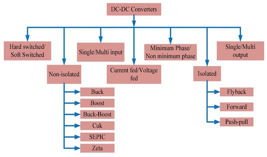
Figure 1. Types of DC-DC converters.
When the traditional boost converter is preferred in PV systems, it has to be operated at a duty cycle of 0.88, making it difficult in practical application due to the limitation of semiconductor devices. Moreover, the boost converters suffer the drawback of high switching voltage stress and reverse recovery issues [14]. The applications of smart grid system are summarized in Figure 2.
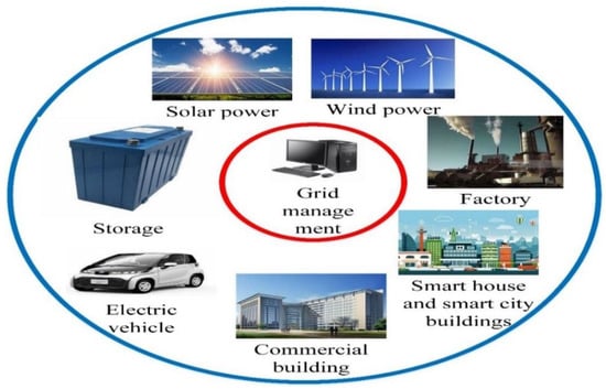
Figure 2. The architecture of smart grid management system applications.
The grid functions today are the same as when there were minor improvements, and the energy cost was relatively low. There is currently no heavy electricity storage technology available. Therefore, if we use this power during off-peak hours, we will build an effective system. However, we may adjust load consumption to increase grid efficiency, which is how the Smart grid differs from a traditional grid.
These converters require a higher power transformer, as higher power converters cannot use a single switch topology. For example, Half-bridge, push-pull and Full-bridge converters comes under another DC-DC isolated converters which use a minimum of multi-switch. Figure 3 represents a simplified hybrid microgrid charging station for battery-powered electric vehicles.
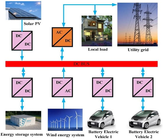
Figure 3. The battery-based electric vehicle’s charging station with the hybrid microgrid model.
The PV technologies can be employed in various applications, including electric vehicles, domestic, and microgrid applications [15]. The different operating voltages of the DC-DC converters linked to the PV system are described. In addition, in grid-connected mode converters, suitable load types are identified along with their corresponding voltage gain and conversion efficiency.
2. Requirements for the Selection of DC-DC Converter Topology
The DC-DC converter topologies that are to be used in a PV-based power supply should meet the conditions given in the subsequent paragraphs. A typical layout of DC microgid is depicted in Figure 4. Without increasing the stack size, we can obtain the desired DC voltage value with the help of the DC-DC converter. For example, the DC output from the polymer electrolyte membrane (PEM) FC stack is mostly around several tens of volts. Therefore, the ripple current value observed across the PV due to the DC-DC converter switching should be low. Most importantly, a sharp rise or a fall in the current and high-frequency current ripple of a large magnitude should be avoided [16].
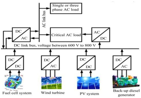
Figure 4. Layout of DC microgrid.
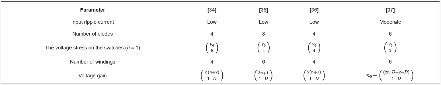
An overview of the present-day technology in isolated DC-DC converters for PV-based power generation is presented in Table 1. The study includes an analysis of literature to understand current achievements and viewpoints. While many papers on the subject have been published, many of them do not include details on the achieved efficiency or the complexity of the converter when operating a greater number of devices, and issues with power density maximization are mentioned. Within the limited information available, a comparison of published literature for high voltage gain DC-DC converters is attempted, and an overview of each solution is provided.
3. Survey of DC-DC Converter Topologies
3.1. Coupled Inductor Converter Topology
This section enumerates the published solutions of coupled inductor topology DC-DC converters possess high gain, as shown in Figure 5, Figure 6, Figure 7 and Figure 8. Each published technique explains the topology used, the converter Vin and Vout range, and the power range of the experimental setup are given to validate the interfacing with FC for power generation. In [17] the authors proposed a DC-DC converter with soft switching exhibits continuous input current and a high voltage gain. Experimentally, a 200 W prototype having Vin = 24 V, and Vout = 360 V gives 96.4% efficiency at full load. The advantages of derived interleaved boost converter having Winding-Cross-Coupled Inductors (WCCIs) and passive-lossless clamp circuits are increased voltage gain, reduced switching voltage stress, and reduced reverse recovery problem due to the leakage inductance when compared with conventional interleaved boost converters [18]. An interleaved boost converter rated 1 kW, 40 V to 380 V experimental findings show an efficiency of 90.7% at full load, which is 5% better than a typical interleaved boost converter. [19]. A three-winding coupled inductor produced a high voltage gain. The energy in the leakage inductor is released to the output directly, reducing the switch stress. The output diode’s reverse recovery current is evaluated using a coupled inductor. A closed loop control method is used, which overcomes the power source voltage drift problem. The converter is used with a FC which gives a Po = 300 W Vout = 400 V, Vin = 27 V–36.5 V and Fs = 100 kHz. It gives a maximum efficiency of 95.2% at 220 W. A 200 W boost converter having coupled inductors, and buck-boost active clamps for low Vin applications is proposed in [20]. The Vin range is 25–40 V, Vout is 200 V and output current of 1A with a switching frequency of 66 kHz. ZVS turns on the main and auxiliary switches, and the boost diode is turned on DC-DC ZCS. Thus, the switching losses are chopped. The converter efficiency is 92%, and the output power is 200 W. A high voltage gains 250 W non-isolated DC-DC converter having a three-stage switching cell and voltage multiplier is proposed and demonstrates the Vin range is 30–45 V, and Vout is 400 V. The three-stage switching cells reduce the converter’s size and conduction losses while efficiency is 97% [20].
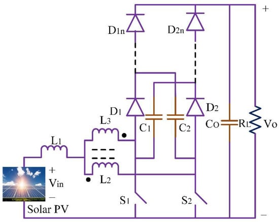
Figure 5. Coupled inductor 1.
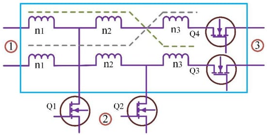
Figure 6. Coupled Inductor 2.
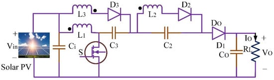
Figure 7. Coupled Inductor 3.
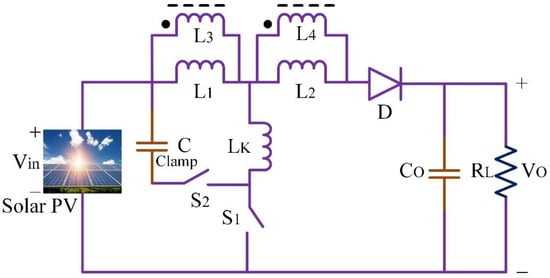
Figure 8. Coupled inductor 4.
A high step-up DC-DC converter is required to boost the voltage value generated through the 400 V DC bus voltage PV. Passive loss clamped technology is used to improve efficiency and limit voltage stress. Recycling of leakage energy is possible with the help of passive losses clamped technology. The basic boost converters’ main disadvantages include problems with the electromagnetic interface, high voltage stress and hard switching on the semiconductor elements [21]. Coupled inductor DC-DC buck-boost converter is used for a step up and down by non-inverting voltage, this also offers high efficiency, control and regulation of input and output currents smoothly and immediately [22].
Table 1. Hybrid converters with observations.
| Ref | Type of ASD | Converter Type | Supply Direction | Observations |
|---|---|---|---|---|
| [22] | Supercapacitor | Buck-boost | Buck-boost | The construction and design are simple, using the same modules for all the positions in the system. |
| [23] | Supercapacitor and Batteries |
Buck-boost | Bidirectional buck-boost |
The buck and boost modes of operation in the buck-boost converter connected with an FC, the operational dead-zone description, is not present in the system. It also consists of a design with complex control |
| [24] | Supercapacitor | Boost | Bidirectional buck-boost |
The experimental result of the boost converter is not present in the system, and the converter also has some start-up problems. |
| [25] | Supercapacitor | Boost | Bidirectional buck-boost |
The experimental load transient results of the boost converter are not present, and the converter has start-up problems. |
| [26] | Supercapacitor | Boost | Bidirectional buck-boost |
The converter consists of a design with complex control, and the converter has start-up problems. |
| [27] | Supercapacitor | Boost | Bidirectional buck-boost |
The boost converter consists of a design with complex control, and the converter has start-up problems. |
The structure of the DC-DC boost converter consists of two hybrid, multiple voltage cells, and three winding coupled inductors. Using two multiple voltage cells, parallelly charged and discharged series, can provide very high voltage gain under the appropriate turns of ratio and duty cycle [28].
3.2. Interleaved Non-Isolated Topology
This section listed the published solutions of high gain interleaved non-isolated DC-DC converter topology. The voltage multiplier technique is used to the non-isolated DC-DC converters to possess a high step-up static gain, is presented in [29]. The Vin is 24 V, and the output Vout is 400 V. The output power is 400 W. The converter operated with a switching frequency of 40 kHz. The converter efficiency was 95%. Low electromagnetic interference production and commutation losses are attained. Without a power transformer, high static gain operation is possible. The Vin is 48 V and Vout is 380 V with an operating frequency of 100 kHz. The measured efficiency at 1 kW is 94.1%. The voltage doubler circuits increase the operating range of the converter by reducing the transformer’s parasitic capacitor’s effects. The interleaved Inductor-Inductor-Capacitor (LLC) converter for high gain is shown in Figure 9. This converter operates in two modes: independently and simultaneously. At the same frequency, both the interleaving converters are operated in the simultaneous mode. The single converter only operates in the independent mode.
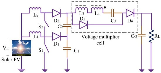
Figure 9. Interleaved non-isolated topology.
The wider Vout range is possible only with frequency control and combined mode changing [30]. The phase-shedding technique is used to improve the efficiency of the interleaved switched capacitor DC-DC converter. The high voltage gain is achieved in the converter with modular characteristics and an interleaved configuration [31]. Using the lower voltage rating, the MOSFETs in the converter reduce the conduction losses [32]. The typical schematic layout is shown in Figure 10.
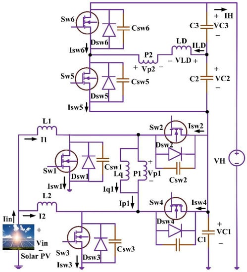
Figure 10. Non-isolated high voltage gain ratio interleaved coupled-inductor type DC-DC converter.
All diodes and switches operate on ZVS and ZCS techniques in the interleaved full soft-switching DC-DC converter. To reduce the power loss and to increase the efficiency of the DC-DC converters, the ZVS and ZCS are used. Finally, the auxiliary circuit is placed out of the main power path to avoid the switches’ high current and voltage stress [33]. The schematic circuit diagram of interleaved high step-up converter is depicted in Figure 11. A highly efficient power system always insists a reliable DC-DC converter. An interleaved boost converter is required to convert the high-current low-voltage to low-current high-voltage.
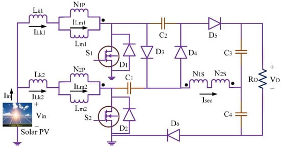
Figure 11. High step-up interleaved converter.
Classical boost converter deemed to be less advance then interleaved boost converter which offers high efficiency, low input ripple current, fast transient response, high reliability and less electromagnetic emission. Interleaved boost converters are suitable for the design of a highly efficient FC power system. To improve the system efficiency three-phase directly coupled interleaved boost converter using CoolMOS transistor and silicon carbide diode is used. Analysis based on the performances of interleaved converters are summarized in Table 2.
Table 2. Performance analysis of the interleaved converters.
This entry is adapted from the peer-reviewed paper 10.3390/en15207569
This entry is offline, you can click here to edit this entry!