Your browser does not fully support modern features. Please upgrade for a smoother experience.
Please note this is an old version of this entry, which may differ significantly from the current revision.
Class D power amplifiers, one of the most critical devices for application in sound systems, face severe challenges due to the increasing requirement of smartphones, digital television, digital sound, and other terminals. The audio power amplifier has developed from a transistor amplifier to a field-effect tube amplifier, and digital amplifiers have made significant progress in circuit technology, components, and ideological understanding. The stumbling blocks for a successful power amplifier are low power efficiency and a high distortion rate.
- class D audio amplifiers
- GaN device
- power efficiency
1. Introduction
The power amplifier is a type of electronic amplifier designed to increase the magnitude of the power of a given input signal. The audio power amplifier circuit is an essential branch of the power amplifier, one of the essential components of a sound system. It is designed as a final block in an audio amplifier chain to increase the input signal to a level that is high enough to drive loads. It has come a long way under the influence of the rapid development of integrated circuits in recent decades.
The audio power amplifier market is driven by the increasing demand for mobile audio devices, the growing prevalence of consumer electronics devices worldwide, the growing appeal of in-car infotainment systems, and the growing market for high-quality audio devices. According to the report by [1], “The audio amplifier market size is expected to grow from USD 3.4 billion in 2019 to USD 4.4 billion by 2024, at a CAGR of 5.6% from 2019 to 2024”. A larger market makes upgrading and improving audio amplifiers very meaningful.
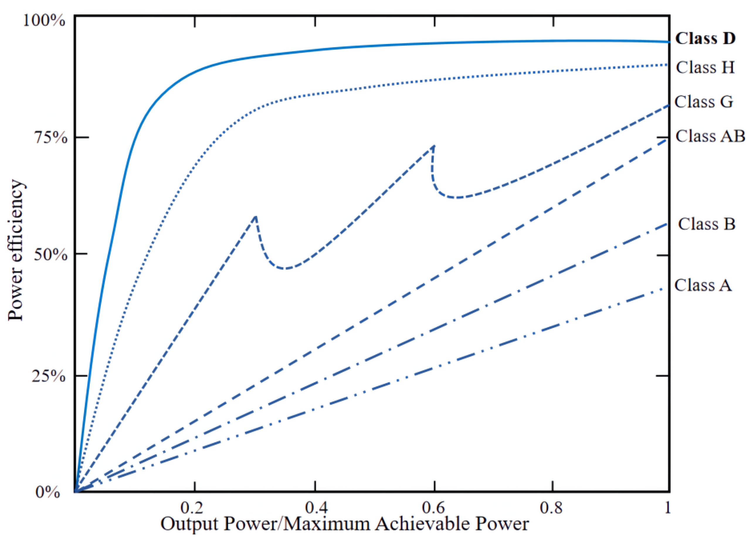
The power efficiency comparison of audio amplifiers is shown in Figure 1. Traditional analog power amplifiers can be classified into Class A, Class B, Class AB, and other forms according to different working conditions. These kinds of amplifiers have high fidelity, which means they can provide superior sound quality. However, the power conversion efficiency of linear and non-linear amplifiers is extremely low. The emergence of Class D amplifiers solves this problem. The Class D amplifier was first devised in 1958 [2]. Compared to linear power amplifiers (Class A) and non-linear amplifiers (Class AB, Class B, Class C) [3][4], the primary advantage of switching-type Class D amplifiers is their theoretical 100% power efficiency [5]. The power efficiency of Class D amplifiers at a maximum modulation index is typically higher than 90% [6]. In contrast, the power efficiency of linear amplifiers such as Class B and Class AB power amplifiers was only 70% or less. This is why the Class D amplifier is currently the best choice for commercial audio amplifiers and is gradually replacing linear counterparts [7].
The switching device in the output stage is the main point in the history of Class D amplifier development. Germanium transistors were a part of early Class D amplifier design but proved unsuitable for switching topology, hence, early amplifier designs were unsuccessful. Nevertheless, thanks to the advent of MOSFET technology, the relative technology of Class D design was again developed by engineers. The Class D amplifier is currently widely used in various fields such as flat-screen televisions and car sound-control units. Class D amplifiers use a pair of switching devices for push/pull configuration.
The performance of the switching device directly affects the power efficiency and high fidelity of the audio system. Due to the limitation of material characteristics, it is difficult to improve the overall performance of existing silicon-based devices by improving the device structure and manufacturing process [5][10]. Therefore, new high-performance power devices are needed as substitutes to achieve better conversion efficiency, which requires minor conduction and lower switching losses to suit variable frequency occasions.
2. Topologies for Class D Amplifiers
The amplifier’s topologies are the basic structure that depends on the work mode and parameters such as power efficiency and degree of distortion. Researchers analyze the Class D amplifier’s topological model to determine the advantages and disadvantages, lists standard amplifier design examples, and provides the basis for improving the amplifier.
A widespread closed-loop analog Class D amplifier covers integrators, modulators, output stage, low-pass filters, and loudspeakers (Figure 2). In the first step, integrators and filters provide high loop gain and attenuate unwanted carrier components in the loop. The low-pass filter is always designed between the output model and the loudspeaker to decrease EMI (electromagnetic interference) and exclude extraordinary frequency energy, which is transformed to [11][12].
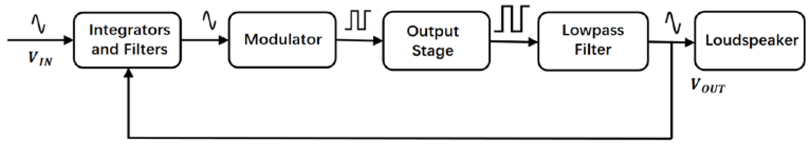
Figure 2. Block diagram of an audio amplifier.
The transistors operating in the saturation or linear region limit the power efficiency of a linear amplifier due to the significant voltage drops that are caused by the large current, resulting in a substantial power loss that greatly influences the efficiency. Class D amplifiers have a unique topology that dissipates less power than the linear amplifiers mentioned above. The output stage works by switching between positive and negative and producing a series of voltage pulses, while the output transistor has no current without switching and low VDS when managing the current, thus forming smaller IDS [13]. The topologies of Class D amplifiers are shown in Figure 3a; analog audio signals are sampled and pulse-width-modulated signals are generated. These signals are used to drive the output switches. The signals generated by the output stage will be filtered by the filtering circuit or the speaker itself and converted into sound signals.
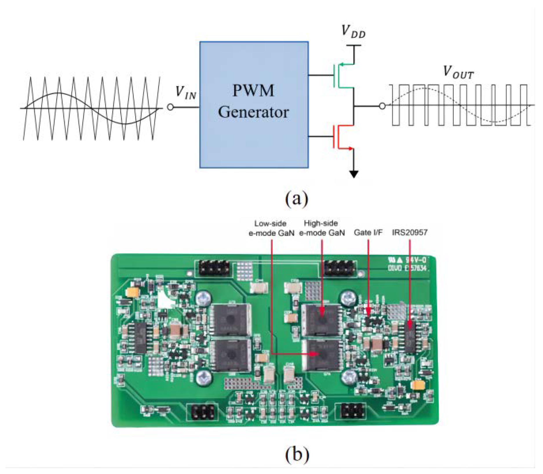
Figure 3. The topology and wave (a) form for Class D amplifier and GaN-based design (b) [14].
The Class D amplifier’s performance is outstanding at the medium and high-power output. However, because of the losses in power devices, the efficiency is lowest if the power output is inadequate. Some Class D amplifiers operate in two modes to overcome this challenge. The multistage technique limits the output voltage to which the power device can switch if playing low-volume audio. Once the output volume reaches a set threshold, the output voltage rail of the switch is increased to provide a complete voltage swing. Zero voltage switching (ZVS) technology can be used at a low output and hard switching at high-power levels to help reduce the impact of switching losses [15][16].
The output stage is the foundation of the power amplifier. Figure 4 shows an essential CMOS (complementary metal oxide semiconductor) linear switch output stage, which amplifies the signal current into a large current that can drive loudspeakers by adding the energy of DC to the slight wind to the input through the triode. In traditional transistor amplifiers, the output stage contains a transistor that provides a continuous instantaneous output current. Many audio linear amplifiers contain Class A, Class AB, and Class B amplifiers. Compared to digital amplifiers and Class D amplifiers, the power consumption is significant even in the most efficient linear region. This diversity makes Class D amplifiers hugely beneficial in many applications. Lower power consumption generates less heat, saves space and cost, and extends the service time of mobile systems.

Figure 4. CMOS linear switch output stage.
3. GaN-Based Class D Amplifier
In the case of mobile devices with limited battery capacity, working efficiency is a crucial design metric. Although the Class D amplifier has a power consumption advantage over other amplifiers, it still suffers from low fidelity, mainly due to switching distortion.
The processors of Class D amplifiers produce small high-frequency pulse width modulation (PWM) signals that represent the auditory signal. The power transistor converts small signals into significant signals in half-bridge or full-bridge configurations and drives the speaker through a filter. Increasing the adoption frequency and the output stage switching frequency can significantly increase the sound because each pulse is a square wave. Power is wasted by switching losses and conduction losses in each switching cycle, thus, balancing sound quality, operating frequency, and power consumption [17]. Switching loss is another factor that requires proper consideration. Thus, the essential component of the Class D amplifier is the switching device, whose quality directly determines the strength of each indicator of the amplifier (examples are SNR, THD, and TID (transient intermodulation distortion)). Class D amplifiers must employ integrated feedback circuits to compensate for poor open-loop performance, in order to complete the distortion performance goals (THD + N, TIM, and IM) that are required for high-quality sound.
The source of this distortion is the power MOSFETs based on Si. Thus, the primary goal of a progressive Class D amplifier is to improve its switching structure. An excellent choice to for the MOSFET or IGBT is the GaN device or SiC device [18].
3.1. Advantages of GaN Power Device
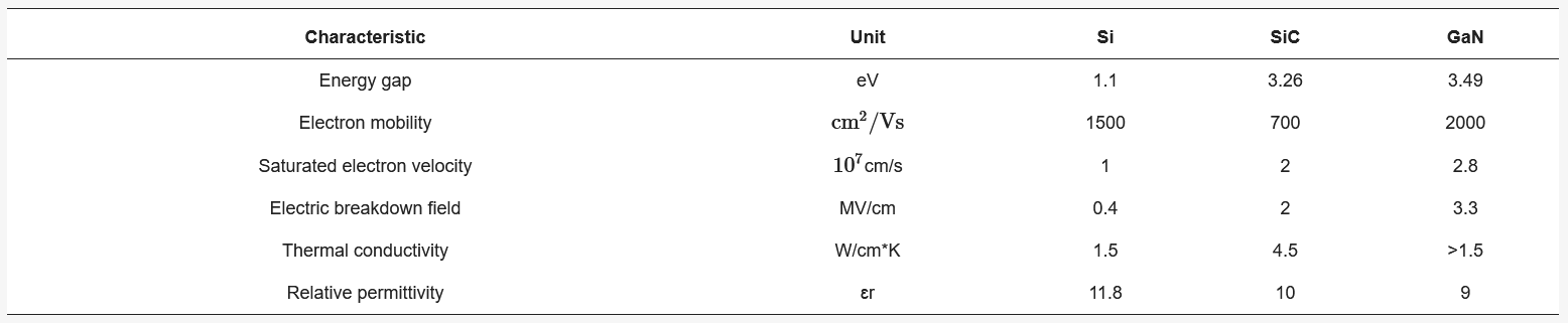
After decades of intensive development, Si-based power devices are approaching their material limits in terms of performance. Power devices based on wide-bandgap semiconductors with a higher critical breakdown field are desired to enhance the device performance further, and thus, the power conversion efficiency. Research on power devices has been ongoing for many years. The advent of wide bandgap (WBG) semiconductors based on gallium nitride (GaN) or silicon carbide (SiC) enables Class-D amplifiers to achieve outstanding performance regarding distortion and bandwidth [19]. According to [20], GaN devices have the advantage of operating at higher voltages and lower leakage currents than Si devices. Compared with the first-generation Si and the second-generation GaAs, the third generation GaN and SiC devices have small on-state resistance, fast switching speed, and high voltage performance. The GaN device has a vacuum saturation rate of 2.8 times that of Si devices, making its on-resistance and conduction losses much lower than Si devices. The common junction capacitance of GaN devices enables its switching frequency up to the Mhz level. The bandgap of the GaN device is much smaller than that of the silicon device, which causes its critical breakdown electric field to be as high as 3.3 MV/cm; therefore, it has a higher voltage capacity. The comparison of parameters between the GaN device and Si device is shown in Table 1. The larger bandgap width and the insulating damaged electric field reduce the device’s conduction resistance and improve its overall performance. The resulting high-electron saturation rate and high carrier mobility enable the device to work at high speeds [21][22]. Moreover, GaN transistors have more applications due to showing higher switching dynamics and incorporating fewer parasitics in their packages. The experiments in [23] demonstrated that GaN devices can lead to a higher power and lower THD in Class D amplifiers. GaN devices play an essential role in many fields, especially in the improvement of power efficiency. It is feasible that these devices could also initiate a revolution in the field of audio power amplifiers [24][25].
Table 1. Comparison of characteristic parameters for various semiconductor materials.
As shown in Figure 5, GaN HEMT transistors are the same as Si MOSFET terminals, with a gate, drain, and source [26]. This also indicates that GaN HEMT has similar functions to Si MOSFET and can substitute for power devices in Class D amplifiers. They achieve meager resistance with the help of a two-dimensional electron gas (2DEG) between the gate and the source and can be effectively short-circuited due to the availability of an electronic pool [27]. The p-Gan gate will stop conduction while there is no gate bias (VGS = 0 V). Gan HEMT is a bidirectional device, unlike silicon devices. Therefore, a reverse current may occur if the drain voltage is permitted to fall below the source voltage. Gan HEMT transistors have the advantage of a clean switching waveform—mainly, the absence of the bulk diodes commonly found in Si MOSFET, which is responsible for much of the switching noise associated with the PN junction [28]. If the amplifier works in zero-voltage switching mode, the switching loss and the power loss can be effectively eliminated because the output transformer is realized by inductance current conversion. At present, most GaN power devices have a planar structure like Figure 5. If the substrate in this structure has minor lattice and thermal mismatch with GaN material, the uneven phase denotative growth of GaN can be implemented. GaN power devices comprising Si material for the substrate have mature technology and low cost, which is the optimal solution of Class D amplifier power devices [29][30].
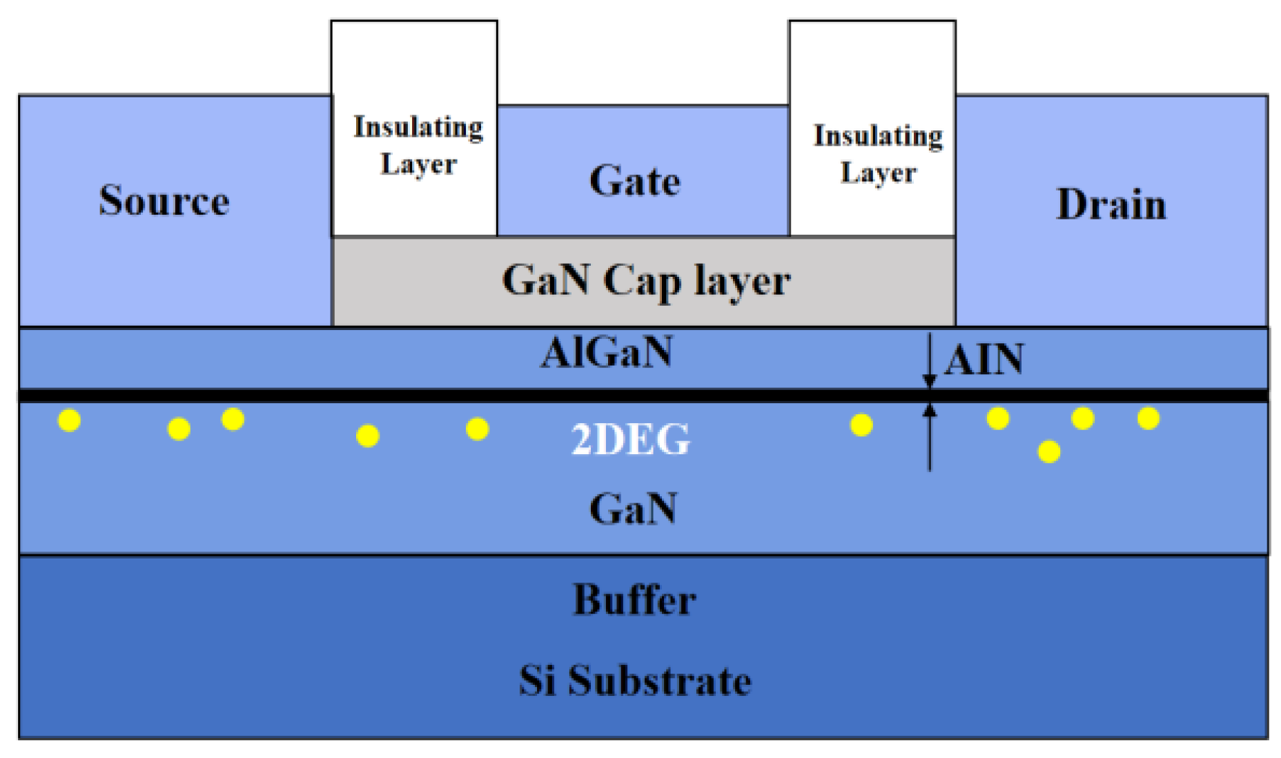
Figure 5. Structure for a Classic GaN HEMT.
3.2. Analysis of GaN Class D Amplifier
Table 2 provides several typical power amplifiers using GaN devices, which are characterized by high power efficiency and low THD. The power density of GaN semiconductors is more than ten times that of the latterly diffused metal oxide semiconductor (LDMOS) transistors used in conventional power amplifiers, with higher power density and efficiency. If researchers use GaN to make IP, they can obtain more power for the same size and a smaller size for the same power. For high power, efficient audio power amplifiers, GaN HEMT using power loss, power density, and response speed are better choices. Compared to traditional Si MOSFETs, GaN HEMTs have a higher rate, cost of arable land, and better performance and thermal efficiency.
Table 2. The parameters of GaN Class D Amplifier.
| Reference | Frequency | Power Efficiency | Modulation Method | THD | Max Ouput (Watt) |
|---|---|---|---|---|---|
| [31] | 13.56 Mhz | 87% | PWM | / | / |
| [32] | 2.3 Mhz | / | PWM | / | / |
| [33] | 100–300 Hz | 95% | PWM | 0.00% | 1.75 w |
| [34] | 6.78 Mhz | 80–81% | PWM | / | 50 |
| [35] | 10 kHz | 38 mW loss | SHEPWM | 0.48% | / |
| [36] | 40 kHz | 97.70% | SPWM Unipolar | 0.23% | 1001.04 |
| [37] | 2 Mhz | 85.80% | Sigma-Delta | 0.02% | 55.27 |
| [38] | 12.288 mHz | 94–97% | Sigma-Delta | 0.50% | 100 |
| [39] | 4–16 kHz | 93% | PWM | 0.60% | 150 |
| [40] | 450 kHz | 93% | / | 0.13% | 40 watt |
| [41] | 25 hz–25 kHz | 94% | PWM | 0.01% | 12.5 watt |
| [42] | 200 KhZ | 94% | PWM | 0.00% | 1.3 kW |
| [23] | 4.8 Mhz | 96% | / | 1% | 10 kw |
Given the critical indicators of Class D amplifiers, GaN devices have corresponding advantages or disadvantages.
3.2.1. Power Efficiency and Distortion
More than one article has mentioned the advantages of GaN devices over MOSFET and IGBT, especially in [40]. Further, in [41], the effect of the 60 V GaN device and Si device Class D audio amplifier is compared, and the conclusion is drawn that the power density of the GaN power device is much higher than the Si device. In [34] is described the effect of GaN transistors in conventional power amplifiers, achieving over 30% power savings and higher power density and efficiency. Compared with traditional Si MOSFET, GaN FET has higher speed, lower cost, and thermal efficiency. Although the Class D amplifier designed in [37] has an efficiency of only 85.8%, this is because the rated circuit of the transistor used in this design is much larger than what the circuit needs, and higher power can be obtained with a more suitable FET.
The power level of Class D amplifiers aims to achieve accurate large-signal replication from small signal sources while reducing energy loss. Better switching properties of the GaN-based FETs produce waveforms that are closer to the desired ideal waveforms than can be achieved by silicon Mofettes. This is an essential benefit of GaN devices, which can switch up to 1000 times faster than silicon FETs. GaN systems’ white paper quantifies this superb audio quality, showing that GaN-based Class D amplifiers can produce total harmonic distortion (THD) as low as 0.004%, compared to 0.015% for silicon products [43][44]. A PDM 25 W Class D amplifier with GaN and Si devices as output stage is tested and compared in [45]. The test results show that when the output power is less than 20 W, the power amplifier’s distortion based on the GaN device is 0.15% lower than that of the power amplifier based on the Si device, and the power efficiency is 15% higher. In addition, at lower switching frequencies (360 kHz), the two output stages’ distortion performance and power efficiency are similar. At higher switching frequencies (>1.1 Mhz), the GaN output stage has considerable advantages [46].
In addition, in zero-voltage switching mode, the output is changed by inductive current commutation. Therefore, any switching loss in the switching device and the resulting power loss can be moved. However, to avoid shoot-through between the two devices, a small blanking delay must be added to ensure that the off-state of the switching period is maintained until the on-state of the next switching period is entered. the output waveform is different from the waveform expected by the PWM output, resulting in audio signal distortion. The blank delay time depends on the output capacitance Coss of the power device used. Compared to Si MOSFETs, GaN transistors have significantly lower Coss, which means that blanking delay time can be minimized, thereby minimizing distortion.
Therefore, power density, power efficiency, and switching frequency advantages indicate that GaN devices will enable a smaller circuit footprint, lower thermal radiation, and long service life, which bridges the direct contradiction between power efficiency and sound quality. However, cost and the lack of a dedicated Class D amplifier integrated circuit are disadvantages of GaN devices.
3.2.2. Thermal Conductivity
Heating is one of the main problems of GaN devices due to the high-power densities. Due to the high conductivity of the SiC, it is a common method of growing GaN on SiC substrate to limit the temperatures of GaN HEMT to no higher than the maximum temperature [3]. Some variations reported across the literature, such as the GaN output stage, introduce performance reduction after high temperature, which is an essential disadvantage of GaN devices [46][47]. However, the growth of GaN involves particular transition layers typically involving alloys of GaN and AlN, which have inferior thermal conductivity because of disorder-induced phonon scattering. In some cases, the performance limiting factor of GaN might be its thermal conductivity as opposed to its electronic properties. Thus, the heat dissipation of audio systems using GaN devices will be one of the following research focuses. The TMT (Thermal Management Technologies) program introduces several cooling technologies of heat management in semiconductors, such as attached cooling and embedded cooling technologies [48][49][50]. The junction temperature of the GaN devices is usually generated at the drain side of the gate, and for this reason, the thermal management solutions should focus on the heat area.
In [51][52], near-junction embedded microfluidic cooling methods are recommended, which have an excellent effect. This technology is already suitable to replace traditional passive remote cooling techniques.
In [52], the feasibility of using diamond as a substrate for GaN devices was investigated. In [53], diamond microfluidics-based intrachip cooling was used to influence the heat outflow from a model with low thermal conductivity. In addition, the cooling effects of active and passive cooling techniques on GaN devices with SiC as substrate and diamond as substrate were studied in [54].
3.2.3. EMI
The high switching speed of GaN devices will deteriorate the EMI in the amplifier. There have been many articles studying the EMI produced by GaN in converters and its effects, for example [55][56][57][58][59]:
Compared with the Si MOSFET, the full-speed (more than 100 MHz) GaN device increases the EMI to 10 dB. Some EMI reduction schemes are proposed, such as selecting the original [60], modifying the topology of the converter circuit [59], or improving the filter [59]. The research on audio amplifiers is still insufficient at present:
In [60], audio amplifiers were built using the SPICE models of fundamental drivers and GaN transistors, which allow an accurate GaN power stage. Moreover, the research hypothesizes that the model and the object may not be accurate; this error occurs in the low-frequency band. The reason is that the simulation model produces significant spikes of drain currents at the beginning of transistors turning on. In [61], a simple method for the conductive EMI modeling of integrated Class D amplifiers is shown. However, the work does not consider the control circuits of GaN transistors.
The influence of the transistor’s current spikes on the EMI level grows with increasing frequency. Higher switching frequencies flatten the interference spectrum in the entire measurement band for both modulated signals and signals with no modulation. The influence of stray parameters also increases.
This entry is adapted from the peer-reviewed paper 10.3390/electronics11193244
References
- MarketsandMarkets. Audio Amplifier Market by Channel Type (Mono, Two, Four, Six), Device (Smartphones, Television Sets, Desktops & Laptops, Home Audio Systems, Professional Audio Systems, Automotive Infotainment Systems), End-User Industry, Region—Global Forecast to 2024. 2019. Available online: https://www.marketsandmarkets.com/Market-Reports/audio-amplifier-market-187106441.html (accessed on 25 July 2022).
- Gaalaas, E. Class d audio amplifiers: What, why, and how. Analog. Dialogue 2006, 40, 1–7.
- Hamza, K.H.; Nirmal, D. A review of GaN HEMT broadband power amplifiers. AEU-Int. J. Electron. Commun. 2020, 116, 153040.
- Fu, Z.; Anttila, L.; Abdelaziz, M.; Valkama, M.; Wyglinski, A.M. Frequency-Selective Digital Predistortion for Unwanted Emission Reduction. IEEE Trans. Commun. 2015, 63, 254–267.
- Jiang, X. Fundamentals of Audio Class D Amplifier Design: A Review of Schemes and Architectures. IEEE Solid-State Circuits Mag. 2017, 9, 14–25.
- Texas Instruments. TPA2037D1—3.2W Mono Class-D Audio Power Amplifier With 6-dB GAIN and Auto Short-Circuit Recovery; Texas Instruments: Dallas, TX, USA, 2010.
- Kwon, S.; Kim, I.; Yi, S.; Kang, S.; Lee, S.; Hwang, T.; Moon, B.; Choi, Y.; Sung, H.; Koh, J. A 0.028% THD+ N, 91% power-efficiency, 3-level PWM Class-D Amplifier with a True Differential Front-End. In Proceedings of the 2012 IEEE International Solid-State Circuits Conference, San Francisco, CA, USA, 19–23 February 2012; pp. 96–98.
- Hood, J.L. Simple Class A amplifier: A 10-W design giving subjectively better results than Class B transistor amplifiers. Electron. World 2004, 110, 44–49.
- Velasco-Quesada, G.; Roman-Lumbreras, M.; Perez-Delgado, R.; Conesa-Roca, A. Class H Power Amplifier for Power Saving in Fluxgate Current Transducers. IEEE Sens. J. 2016, 16, 2322–2330.
- Yang, F.; Xu, C.; Akin, B. Experimental Evaluation and Analysis of Switching Transient’s Effect on Dynamic on-Resistance in GaN HEMTs. IEEE Trans. Power Electron. 2019, 34, 10121–10135.
- Takagishi, H. Class D Audio Amplifier. U.S. Patent US6489841B2, 3 December 2002.
- Kim, J.; Roblin, P.; Chaillot, D.; Xie, Z. A Generalized Architecture for the Frequency- Selective Digital Predistortion Linearization Technique. IEEE Trans. Microw. Theory Tech. 2013, 61, 596–605.
- Kang, Y.; Ge, T.; He, H.; Chang, J.S. A review of Audio Class D amplifiers. In Proceedings of the 2016 International Symposium on Integrated Circuits (ISIC), Singapore, 12–14 December 2016; pp. 1–4.
- GaNsystems. 500W Heatsinkless Audio Amplifier from Axign and GaN Systems Demonstrates a New World of Extraordinary Audio Performance. 6 January 2022. Available online: https://gansystems.com/newsroom/500w-heatsinkless-audio-amplifier-from-axign/ (accessed on 15 February 2022).
- Hur, J.; Lee, O.; Lee, C.; Lim, K.; Laskar, J. A Multi-Level and Multi-Band Class-D CMOS Power Amplifier for the LINC System in the Cognitive Radio Application. IEEE Microw. Wirel. Compon. Lett. 2010, 20, 352–354.
- Lee, M.J.; Lee, H.N.; Choi, U.G.; Yang, J.R. Multi-level Waveform Generator with Delay Control for Low Distorted Class D Amplifiers. IDEC J. Integr. Circuits Syst. 2021, 7, 2.
- ElectronicDesign.70. GaN FET Technology Solving Audible Challenges For High-Performance Audio Amplifiers. Available online: https://www.electronicdesign.com/leaders/power/power-supplies/article/21174367/gan-fet-technology-solving-audible-challenges-for-highperformance-audio-amplifiers (accessed on 9 September 2021).
- Jones, E.A.; Wang, F.; Ozpineci, B. Application-based review of GaN HFETs. In Proceedings of the 2014 IEEE Workshop on Wide Bandgap Power Devices and Applications, Knoxville, TN, USA, 13–15 October 2014; pp. 24–29.
- Mauerer, M.; Tüysüz, A.; Kolar, J.W. Distortion Analysis of Low-THD/High-Bandwidth GaN/SiC Class-D Amplifier Power Stages. In Proceedings of the 2015 IEEE Energy Conversion Congress and Exposition (ECCE), Montreal, QC, Canada, 20–24 September 2015; pp. 2563–2571.
- Microsemi, P.P.G. Gallium Nitride (GaN) Versus Silicon Carbide (SiC) In the High Frequency (RF) and Power Switching Applications. Digi-Key. 2014. Available online: https://www.richardsonrfpd.com/docs/rfpd/Microsemi-A-Comparison-of-Gallium-Nitride-Versus-Silicon-Carbide.pdf (accessed on 25 July 2022).
- Ueda, T. Recent advances and future prospects on GaN-based power devices. In Proceedings of the 2014 International Power Electronics Conference (IPEC-Hiroshima 2014—ECCE ASIA), Hiroshima, Japan, 18–21 May 2014; pp. 2075–2078.
- Peftitsis, D.; Rabkowski, J. Gate and Base Drivers for Silicon Carbide Power Transistors: An Overview. IEEE Trans. Power Electron. 2016, 31, 7194–7213.
- Nikolaus, P.S.; Anderson, J.A.; Bortis, D.; Kolar, W. Ultra-High Bandwidth GaN-Based Class-D Power amplifier for testing of three-phase mains interfaces of renewable energy systems. In Proceedings of the 2019 8th International Conference on Renewable Energy Research and Applications (ICRERA), Brasov, Romania, 3–6 November 2019; pp. 615–622.
- Ishibashi, T.; Okamoto, M.; Hiraki, E.; Tanaka, T.; Hashizume, T.; Kachi, T. Resonant gate driver for normally-on GaN High-electron-mobility transistor. In Proceedings of the 2013 IEEE ECCE Asia Downunder, Melbourne, Australia, 3–6 June 2013; pp. 365–371.
- Huang, X.; Li, Q.; Liu, Z.; Lee, F.C. Analytical Loss Model of High Voltage GaN HEMT in Cascode Configuration. IEEE Trans. Power Electron. 2014, 29, 2208–2219.
- Rodriguez, M.; Zhang, Y.; Maksimovic, D. High-frequency PWM buck converters using GaN-on-SiC HEMTs. IEEE Trans Power Electron. 2014, 29, 2462–2473.
- Im, K.-S.; Ha, J.-B.; Kim, K.-W.; Lee, J.-S.; Kim, D.-S.; Hahm, S.-H.; Lee, J.-H. Normally Off GaN MOSFET Based on AlGaN/GaN Heterostructure With Extremely High 2DEG Density Grown on Silicon Substrate. IEEE Electron Device Lett. 2010, 31, 192–194.
- Keshmiri, N.; Wang, D.; Agrawal, B.; Hou, R.; Emadi, A. Current Status and Future Trends of GaN HEMTs in Electrified Transportation. IEEE Access 2020, 8, 70553–70571.
- Tfipathy, S.; Vivian, K.X.L.; Dolmanan, S.B.; Tan, P.Y.J.; Kajen, R.S.; Bera, L.K.; Teo, S.L.; Kumar, K.M.; Arulkumaran, S.; Ng, G.I.; et al. AlGaN/GaN Two-dimensional-electron Gas Hetero-structures on 200mm diameter Si(111). Appl. Phys. Lett. 2012, 101, 82–110.
- Blomley, P. New approach to Class B amplifier design. Wirel. World 1971, 76, 57–61.
- Tong, Z.; Ye, Z.; Rivas-Davila, J. Class DE Switch-Mode Power Amplifier Using GaN Power HEMTs: High-Efficiency Power Amplifier for 13.56 MHz. IEEE Microw. Mag. 2022, 23, 72–79.
- Singh, P.; Hariharan, K.; Kapat, S. High-frequency digital current mode control architectures for Class-D audio amplifiers. In Proceedings of the 2022 IEEE Applied Power Electronics Conference and Exposition (APEC), Houston, TX, USA, 20–24 May 2022; pp. 1846–1852.
- Jiang, X.; Song, J.; Cheung, D.; Wang, M.; Arunachalam, S.K. Integrated Class-D Audio Amplifier With 95% Efficiency and 105 dB SNR. IEEE J. Solid-State Circuits 2014, 49, 2387–2396.
- Park, Y.J.; Lee, K.-Y. High-efficiency, High-power Class-D Power Amplifier with 50W Output Using GaN Devices. In Proceedings of the 2021 Twelfth International Conference on Ubiquitous and Future Networks (ICUFN), Jeju Island, Korea, 17–20 August 2021; pp. 44–47.
- Aimaier, N.; Ly, N.; Nobert, G.; Blaquière, Y.; Constantin, N.; Cowan, G. SHEPWM Class-D Amplifier with a reconfigurable gate driver integrated circuit. In Proceedings of the 2021 IEEE International Symposium on Circuits and Systems (ISCAS), Daegu, Korea, 22–28 May 2021; pp. 1–5.
- Alves, A.N.; Praça, P.P.; Júnior, D.D.S.O.; Barreto, L.H.S.C. 1 KW Amplifier Class D Design with GaN Switches (No. 4646). EasyChair, 2020; In print.
- Hafizovic, D.; Magnus, K. GaN Transistor Based Digital Class-D Amplifier with Global Feedback. Master’s Thesis, Chalmers University of Technology, Gottenburg, Sweden, 2020.
- Kassaw, K. Methods of High-Fidelity, High-Efficiency Class-D Audio Amplification. Bachelor’s Thesis, University of Arkansas, Fayetteville, AR, USA, 2020.
- Zaman, H.; Zheng, X.; Wu, X.; Khan, S.; Ali, H. A Fixed-Frequency Sliding-Mode Controller for Fourth-Order Class-D Amplifier. Electronics 2018, 7, 261.
- Sangid, J.; Long, G.; Mitchell, P.; Blalock, B.J.; Costinett, D.J.; Tolbert, L.M. Comparison of 60V GaN and Si devices for Class D audio applications. In Proceedings of the 2018 IEEE 6th Workshop on Wide Bandgap Power Devices and Applications (WiPDA), Atlanta, GA, USA, 31 October–2 November 2018; pp. 73–76.
- Sangid, J.M. GaN vs. Si for Class D Audio Applications. Master’s Thesis, University of Tennessee, Knoxville, TN, USA, December 2018.
- Mauerer, M.; Laboratory, E.Z.P.E.S.; Kolar, J.W. Distortion Minimization for Ultra-Low THD Class-D Power Amplifiers. CPSS Trans. Power Electron. Appl. 2018, 3, 324–338.
- Tsai, C.Y.; Wu, T.L.; Chin, A. High-Performance GaN MOSFET with High-κ LaAlO3/SiO2 Gate Dielectric. IEEE Electron Device Lett. 2012, 33, 35–37.
- Gansystems. High-efficiency 200W stereo class-D amplifier & LLC switched mode power supply w/PFC. In GS-EVB-AUD-BUNDLE2-GS Technical Manual; Gansystems: Toronto, ON, Canada, 2021.
- Chung, J.; McKenzie, R.; Ng, W.T. A Comparison Between GaN and Silicon Based Class D audio power amplifiers with pulse density modulation. In Proceedings of the 2016 13th IEEE International Conference on Solid-State and Integrated Circuit Technology (ICSICT), Hangzhou, China, 25–28 October 2016; pp. 90–93.
- Kuzuhara, M. Nitride power devices: Future perspectives. In Proceedings of the International RCIQE/CREST Joint Workshop, Hokkaido University, Hokaido, Japan, 1–2 March 2010; pp. 1–2.
- Flack, T.J.; Pushpakaran, B.N.; Bayne, S.B. GaN technology for power electronic applications: A review. J. Electron. Mater. 2016, 45, 2673–2682.
- Bloschock, K.P.; Bar-Cohen, A. Advanced thermal management technologies for defense electronics. Def. Transform. Net-Cent. Syst. 2012, 8405, 157–168.
- Bar-Cohen, A. Towards embedded cooling-Gen 3 thermal packaging technology. In Cooling of Microelectronic and Nanoelectronic Equipment: Advances and Emerging Research; World Scientific: Singapore, 2015; pp. 421–457.
- Matin, K.; Bar-Cohen, A.; Joseph, J.M. Modeling and simulation challenges in embedded two phase cooling: DARPA’s ICECool program. In International Electronic Packaging Technical Conference and Exhibition, Proceedings of the ASME 2015 International Technical Conference and Exhibition on Packaging and Integration of Electronic and Photonic Microsystems, San Francisco, CA, USA, 6–9 July 2015; ASME: New York, NY, USA, 2015.
- Bar-Cohen, A. Gen-3 thermal management technology: Role of microchannels and nanostructures in an embedded cooling paradigm. J. Nanotechnol. Eng. Med. 2013, 4, 020907.
- Chlieh, O.L.; Papapolymerou, J. Hybrid Integrated Microfluidic Channels on Multilayer Organic Substrate and on Copper for Tuning and Cooling an RF Reconfigurable S-/C-Band GaN-Based Power Amplifier. IEEE Trans. Microw. Theory Tech. 2017, 65, 156–164.
- Altman, D.H.; Anurag, G.; Matthew, T. Development of a diamond microfluidics-based intra-chip cooling technology for GaN. In International Electronic Packaging Technical Conference and Exhibition, Proceedings of the ASME 2015 International Technical Conference and Exhibition on Packaging and Integration of Electronic and Photonic Microsystems, San Francisco, CA, USA, 6–9 July 2015; ASME: New York, NY, USA, 2015.
- Chen, X.; Nazli, D.F.; Kumar, S.; Graham, S. A numerical study on comparing the active and passive cooling of AlGaN/GaN HEMTs. IEEE Trans Electron Devices 2014, 61, 4056–4061.
- Han, D.; Li, S.; Lee, W.; Choi, W.; Sarlioglu, B. Trade-off Between Switching Loss and Common Mode EMI Generation of GaN Devices-Analysis and Solution. In Proceedings of the 2017 IEEE Applied Power Electronics Conference and Exposition (APEC), Tampa, FL, USA, 26–30 March 2017; pp. 843–847.
- Jingjing, S.; Wenjie, C.; Xu, Y. EMI Prediction and Filter Design for MHz GaN Based LLC Half-Bridge Converter. In Proceedings of the 2016 IEEE 8th International Power Electronics and Motion Control Conference (IPEMC-ECCE Asia), Hefei, China, 22–26 May 2016; pp. 297–304.
- Tian, M.; Hao, Y.; Wang, K.; Xuan, Y.; Huang, L.; Sun, J.; Yang, X. EMI Modeling and Experiment of a GaN based LLC Half-Bridge Converter. In Proceedings of the 2015 9th International Conference on Power Electronics and ECCE Asia (ICPE-ECCE Asia), Seoul, Korea, 1–5 June 2015; pp. 1961–1966.
- Liu, X.; Costa, F.; Revol, B.; Gautier, C. EMI Investigation in a GaN HEMT Power Module. In Proceedings of the PCIM Europe 2016, International Exhibition and Conference for Power Electronics, Intelligent Motion, Renewable Energy and Energy Management, Nuremberg, Germany, 10–12 May 2016; pp. 1–8.
- Morris, C.T.; Han, D.; Sarlioglu, B. A novel inverter topology for reduction of common mode voltage for GaN-based variable frequency inverter. In Proceedings of the 2016 IEEE Transportation Electrification Conference and Expo (ITEC), Dearborn, MI, USA, 27–29 June 2016; pp. 1–6.
- Gedz, O.; Lazebnyi, V.; Onikienko, Y.; Vlasjuk, A. EMI Simulation of GaN power stage for audio Class D amplifiers. In Proceedings of the 2018 14th International Conference on Advanced Trends in Radioelecrtronics, Telecommunications and Computer Engineering (TCSET), Lviv-Slavske, Ukraine, 20–24 February 2018; pp. 204–207.
- Onikienko, Y.; Pilinsky, V.; Vasilenko, O. Modified approach for EMI estimation of integrated Class D amplifiers. In Proceedings of the 2017 IEEE 37th International Conference on Electronics and Nanotechnology (ELNANO), Kyiv, Ukraine, 18–20 April 2017; pp. 443–446.
This entry is offline, you can click here to edit this entry!