Your browser does not fully support modern features. Please upgrade for a smoother experience.
Please note this is an old version of this entry, which may differ significantly from the current revision.
Subjects:
Engineering, Electrical & Electronic
Among cryogenic microwave detectors and bolometers, the superconductor–insulator–normal metal–insulator–superconductor (SINIS) detectors are promising candidates for practical applications due to their wide dynamic range, low requirements for temperature stabilization, lack of upper limit for signal frequency, and immunity to vibrations and magnetic fields compared to competing cryogenic detectors such as transition edge sensors, kinetic inductance detectors, hot electron detectors, and SIS detectors.
- SINIS structures
- superconductivity
- thin-film technology
- tunnel junctions
1. Introduction
Normal metal–insulator–superconductors (NISs), as well as SIS tunnel junctions, are the main building blocks in superconducting electronics. SINIS is one of the generic elements of a wide family of cryogenic devices [1,2,3], such as Andreev bolometers (AB) [4,5], normal metal hot-electron bolometers (NHEB) [6], cold-electron bolometers (CEB) [7,8], SINIS bolometers [9,10,11], SINIS detectors [12,13,14], NIS array thermometers [15,16,17], electron coolers [18,19,20,21], and photon counters. Over the 30 years in which they have been in development, detectors with NIS tunnel junctions have been referred to as ANHEB—a normal metal hot-electron bolometer with Andreev reflection (SNS + NIS), actually operating at frequencies below 70 GHz; CCNHEB [22]—capacitive coupled normal metal hot-electron bolometers (SINIS); CEB—cold-electron bolometers (SINIS), which are the same as CCNHEB, but operate with electron cooling; SINIS detectors—an SINIS structure in the operation mode of quantum response, at frequencies above 70 GHz; an NISIN detector with a structure similar to SINIS, or even NININ or MIMIM detectors with metal–insulator–metal tunnel junctions [23,24].
A hot-electron bolometer with Andreev contacts between the N-absorber and S-electrodes, and with an NIS thermometer for temperature response measurement, was proposed in a publication [5]—see the schematic view in Figure 1. Such a bolometer demonstrated, under dc heating, a responsivity of up to 109 V/W and a noise equivalent power (NEP) = 3 × 10⁻¹⁹ W/Hz1/2.
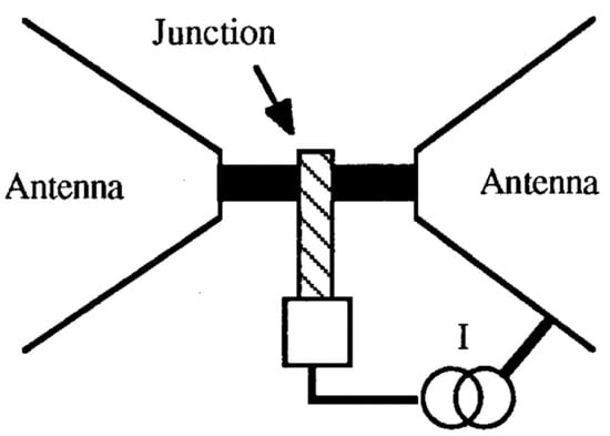
Figure 1. Basic schematics of ANHEB with superconducting antenna directly connected via Andreev junctions to normal metal absorber (black), and NIS junction thermometer connected to current source I.
One of the first attempts to study ANHEB bolometers (Figure 2) under microwaves was made in [4], in which, under dc heating, NEPdc = 5 × 10⁻¹⁸ W/Hz1/2 was obtained and at 300 GHz irradiation, only NEPmicrowave = 10−14 W/Hz1/2 and dV/dP = 106 V/W were reached, whose values are much lower compared to the response at dc or low frequencies.
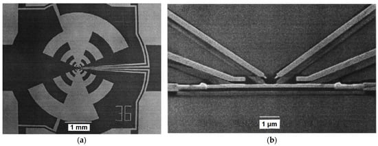
Figure 2. SEM view of ANHEB integrated in log-periodic mode (a) and a microbolometer (b) [4].
The reason for this contradiction is that Andreev contacts are transparent to electrons with energy above the superconducting aluminum gap, which is about 70 GHz. This became clear in 2001 after theoretical analyses performed by Devyatov. A solution to increasing the signal frequency was found by Likharev, who proposed replacing the Andreev contacts with tunnel NIS junctions. The first practical results of an SINIS microwave detector were obtained in 2001 at Chalmers University of Technology [22], and these are described in detail in [25].
In the same year, pioneering work on electron cooling using NIS junctions appeared [26,27]. As Devyatov noted, since the NIS junction provides electron cooling, such cooling can also occur in the bolometer, so under certain modes of operation of the SINIS structure, it can switch from a hot-electron bolometer (HEB) operation mode to a cold-electron bolometer (CEB) mode, as was first proposed in [28]. In such a bolometer, at a dc bias close to the energy gap, it is possible to obtain electron cooling from the phonon temperature of 300 mK down to the electron temperature of about 100 mK, thus theoretically reducing the dc NEP to 10−18 W/Hz1/2.
Depending on the frequency range and the required bandwidth, the designs of bolometers with different planar antennas were fabricated and experimentally studied. Such integrated antenna–SINIS structures were assessed in quasioptical lens systems, and optical response values up to 0.8 × 10⁹ V/W and NEP = 2 × 10⁻¹⁷ W/Hz1/2 were obtained at frequencies around 350 GHz.
2. Fabrication Technology of SINIS
Depending on the available equipment and tasks, different methods of aluminum tunnel junction fabrication can be used. These methods can be divided into two main types: shadow evaporation at tilted angles (Table 2) and direct deposition (Table 3).
Table 2. Comparison of two main shadow technologies for the fabrication of Al tunnel junctions.
| Shadow Technique | ||
|---|---|---|
| Dolan’s Bridges | Bridge-Free Technology | |
| Short description |
|
|
| Schematic image of process |  |
 |
| Advantages | Deposition in one vacuum cycle, one lithography | Deposition in one technological process—this technology overcomes the disadvantages of Dolan’s suspended bridges |
| Disadvantages | Possibility of breaking the suspended resist bridge, not completely removing vertical walls, possibly bending the upper layer of the resist; only e-beam lithography; specialized deposition equipment | The common drawback for both shadow evaporation methods is that they require directional evaporation and are not applicable for magnetron sputtering; only e-beam lithography; specialized deposition equipment |
Table 3. Comparison of different direct-write technologies for the fabrication of tunnel junctions.
| Direct-Write Technology | ||
|---|---|---|
| Direct-Write Trilayer Technology | Direct-Write Technology | |
| Short description |
|
|
| Schematic image of process | 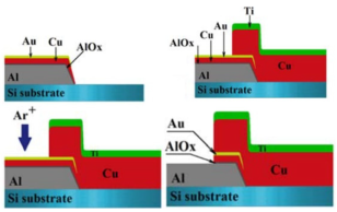 |
 |
| Advantages | Any type of lithography | Can be applicable for industrial processes of magnetron sputtering and plasma etching. Such process bring flexibility in the choice of metal film materials and the possibility of creating a high-quality tunnel barrier. Any type of lithography |
| Disadvantages | Three technological cycles, additional layers for passivation | Two technological cycles |
2.1. Shadow Evaporation Technology
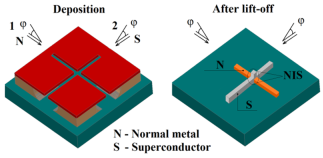
Usually, SINIS structures are fabricated by Dolan’s technology [34] with suspended bridges of e-beam resist (see Table 2, middle column). Deposition at different angles can be achieved by thermal evaporation using the hot boat, or by e-beam evaporation using a crucible on a tilted holder with a substrate. First, the aluminum layer with an underlayer of Fe is deposited at a normal angle to the substrate. The Fe/Al bilayer is a non-superconducting normal metal due to the suppression of the superconductivity of Al by ferromagnetic Fe. The tunnel barrier is formed via a proper dose of oxygen in the deposition chamber. The top superconducting aluminum layer is deposited at a tilt angle ± 45°. This process can be modified for different angles and thicknesses of both resist layers, which should be exactly calculated. However, the classical Dolan process with a suspended e-beam resist bridge has two basic disadvantages: it is difficult to fabricate the sub-micrometer-size NIS junctions, and it has low reliability due to the sagging and breaking of thin and narrow suspended resist bridges. To solve these problems, bridge-free technology (Table 2, right column) [35,36] was used for the creation of the SINIS structure. Bridge-free technology allows one to fabricate tunnel junctions with areas from 0.01 μm2 (and less) to 1000 μm2 (and more), improve the size accuracy, increase the reliability and reproducibility, improve the electric conductivity and heat conductivity of the bias wiring via the increase in superconductor thickness, increase the range of exposure dose from 10% to 50%, and increase the possibility of ion cleaning before deposition (there are no thin suspended resist bridges). The key idea of this technology [35,36] is based on the separated deposition of two different metal films into two deep orthogonal grooves in a double-layer resist. The deposition of the first film into the first groove does not lead to deposition in the second groove, because the deposition angle and resist thickness are chosen such that in the deposition into the second groove, the direction is oriented towards the wall of the resist, with subsequent removal together with resist in the lift-off process. Analogously, the second film is deposited into the orthogonal groove when the substrate is rotated by 90°. As a result, only tunnel junctions of the required size remain on the substrate, with the bottom and top electrodes formed along corresponding grooves in the resist. If the sizes of junctions are not large enough, the design can be modified by adding big squares that are slightly shifted towards one another due to the tilt angles and resist thickness.
2.2. Direct Deposition Technology
Shadow evaporation is relatively simple, and allows the depositing of the SINIS structure in one vacuum cycle with one e-beam lithography. However, this method is limited in the dimensions of junctions and in the choice of materials. Besides this, magnetron sputtering is much more widely used, and is the main technology for industrial fabrication. In our earlier work [37], instead of shadow evaporation, we succeeded in fabrication using separate lithography, with a Ti absorber and with magnetron sputtering. The Al technology includes one more step of etching the native aluminum oxide before the fabrication of the tunnel barrier.
All of the technologies that were presented previously have one common feature—the tunnel junction is deposited in one vacuum cycle. This is necessary for the creation of a high-quality tunnel junction. With separate cycles (lithography of one layer and deposition of the first film, and then a similar procedure for the second), the quality of the tunnel junction will be significantly worse due to the fact that uncontrolled parasitic oxides form on the surface of the first film. To solve this problem, we developed a modified direct-write technology [33,38] (Table 3, right column). The idea is to use ion etching before the deposition of the second layer in the deposition chamber. In this case, the layer of aluminum oxide is removed, and it is possible to oxidize the “clean” aluminum layer, or make an additional thin (a few nm) aluminum layer to be oxidized in order to create a high-quality tunnel barrier. Additionally, such technology allows flexibility in the choice of metal film materials.
Photos of the samples fabricated via different technologies are presented in Figure 8a–d.
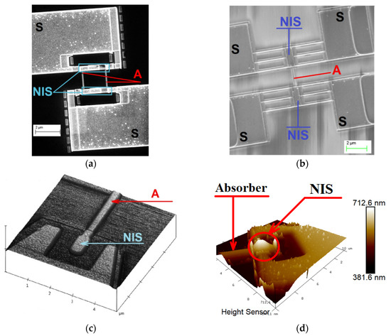
Figure 8. Photos of samples fabricated via different technologies (A—absorber; NIS—normal metal–insulator–superconductor tunnel junction; S—superconducting electrodes): (a) Dolan’s technique; (b) bridge-free technology; (c) direct-write trilayer technology; (d) direct-write separate lithography technology with magnetron sputtering.
2.3. Fabrication of SINIS Junctions with Suspended Absorber
The need to fabricate SINIS detectors with suspended absorbers is increased by the need to reduce power losses to the substrate and to increase the quantum efficiency of the receiver. The first attempt to realize SINIS structures with suspended absorbers were made in [39,40].
For the creation of such types of SINIS, we used different methods: direct deposition and shadow evaporation. The idea of the direct technology [41] is clear: a trilayer comprising Al–AlOx–Cu is deposited directly onto the window and then lifted off. In the next step, with laser or e-beam lithography, we open the window in the area where part of the absorber will be suspended. The etching of normal metal Cu in nitric acid around the superconducting electrodes follows; this additional step allows the improvement of the IV curve, and shows the correct position of the energy gap voltage to be 400 mV. However, this additional step reduces the yield of samples, and it is only possible when using Cu as the absorber. The disadvantage of Cu is that it is rather soft, and it can sag when it is relatively long (a few micrometers). For a schematic image and photo of the SINIS detector with a suspended absorber, see Figure 9.
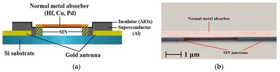
Figure 9. Schematic image (a) and photo (b) of SINIS detector with suspended absorber.
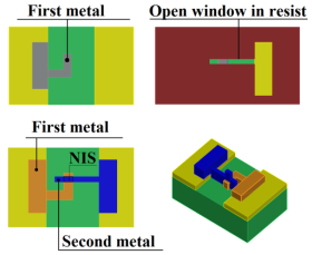
To avoid the chemical etching of a normal metal, we developed a process involving the shadow evaporation of the normal metal in the required area. A schematic view of this fabrication process is presented in Figure 10. This technology requires rather thick resists of over 900 nm. The absorber film is only deposited in the wider area, and in narrow (about 1 μm wide) areas, the metal is evaporated onto the wall of the resistor, before finally being removed together with the resist in the lift-off step. The process of Al with bridge etching is the same as in the previous process using Cu. SEM views of such samples are presented in Figure 11.
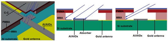
Figure 10. Schematic view of the process with the shadow evaporation of the normal metal in the required area [33].
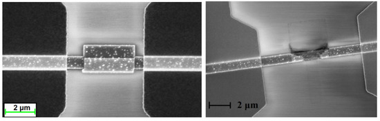
Figure 11. SEM images with examples of SINIS detectors with a suspended Hafnium absorber before (left) and after (right) aluminum etching under the absorber [33].
3. Applications of SINIS Detectors
Sub-terahertz detectors are intended for applications in various fields of science [44,45,46], astronomy [47,48], technology, commercial applications, telecommunications [49,50,51], military applications [52,53,54], security systems, and life sciences. Astronomy sets the highest requirements for detector sensitivity and wide dynamic range, as primarily this is fundamentally important for ground-based observatories. In telecommunications, there is an urgent need to improve the performance of telecommunications channels, which can be solved by moving from the current satellite communications and mobile communications from centimeter waves to shorter waves. The growing demand for high-speed wireless channels has indicated a trend towards an increase in the signal frequencies towards 24–100 GHz for 5G, 140 GHz, 220 GHz, and 340 GHz for 6G, and 700 GHz suggested for 7G [55]. The optical range is poorly suited for creating cellular data transmission networks due to the suppression of transmission in rain, snow, and fog. Moreover, sub-THz telecommunications can be used to create secure communications for military applications. In radar systems, two areas can be distinguished: military applications (aircraft detection and the detection of anti-personnel mines), and a relatively new “problem”—the detection of space threats (such as asteroid–comet hazards, space debris, and space weather).
This entry is adapted from the peer-reviewed paper 10.3390/app122010525
This entry is offline, you can click here to edit this entry!