In the new age of illumination, light emitting diodes (LEDs) have been proven to be the most efficient alternative to conventional light sources. Yet, in comparison to other lighting systems, LEDs operate at low temperatures while junction temperature (Tj) is among the main factors dictating their lifespan, reliability, and performance. Tj may be indirectly measured using an LED’s inherent optical characteristics. The emission spectrum of a semiconductor device is influenced by temperature variations due to the temperature dependence of the energy band gap. This behavior motivates researchers to use spectral power distribution (SPD) characteristics such as the peak wavelength and spectral bandwidth of LEDs, which are known as temperature sensitive optical parameters (TSOPs), to estimate Tj.
1. Introduction
The temperature rise has been an indispensable part of light generation systems. This might explain why we continue to distinguish visible light colors by the temperature of an ideal black-body radiator of a color comparable to that of the light source [
1]. Thermal challenges of light generation systems date back to 125,000 years ago as anatomically modern human beings controlled fire for sources of heating and illumination [
2,
3], dealing with torches, cressets, and bonfires which burnt at near 1000 °C [
4]. Illumination relied on the control of flame and burning fuels created from olive and seed oils, animal grease, tallow, and gas till the 18th century [
5]. In the 19th century, rapid progress in electrical science laid the foundation of modern progress in lighting [
6,
7]. Still, temperature rise was a major challenging part of light generation. From 1835 after the first constant electric light demonstration by Charles Wheatstone, it took 40 years for scientists to figure out how to prevent the 3000 K filament from oxidizing [
8]. Interestingly, from 1924 to 1940, as the lifetime of lightbulbs started to exceed 1800 h, financial agreements led to thermally controlled life-span engineering for added profits [
9]. In 1986, the invention of the first nitride-based blue light emitting diode (LED) by Isamu Akasaki and others eventually revolutionized the lighting industry, allowing high power and efficient solid state lighting [
10]. This breakthrough followed by a rapid optimization process in LED device production led to a cost/lumen reduction of 10-fold and a lumen per LED package increment of 20-fold in each decade [
11]. In terms of efficacy, fluorescent lamps, despite being able to operate at almost room temperature and possibly having the longest lifespan, cannot compete with LEDs [
12]. In addition, LEDs have shown the potential to go beyond the “replacement paradigm” by providing a critical advantage in transportation, display and imaging systems, communications, agriculture, and other fields with their advanced color control and modulation capabilities [
13,
14].
The wavelength of the emission could be engineered with band gap control of the materials in the diffusion region between the p-type and n-type regions of an LED, within a few microns near the p-n junction (λ = 1240/E
g nm) [
15]. LEDs are now capable of photon emission in all visible light wavelengths by progressing from ternary (GaAs
1-xP
x) material selection to quaternary compositions (AlGaInN). AlGaAs material systems are used for infrared and red emission, AlGaInP for amber, orange, and yellow-green, and AlInGaN for green to near ultraviolet. Because of their high thermal conductivity, electron saturation drift velocity, critical breakdown voltage, and fracture toughness to resist defects growth, group III nitride materials are ideal for unlocking the higher powers in LEDs [
16,
17]. However, given the fraction of input power of previous lighting technologies and the highest power conversion efficiency of any known man-made light source, why is it challenging to keep them working at low temperatures?
LEDs (along with all other power semiconductor devices) act as discrete heat sources, dissipating heat through electronic packages into printed circuit boards (PCBs) and heat sinks. Currently, in optimum current densities of LEDs, around 70% of the input electrical power converts into heat generation [
18].
Figure 1a schematically shows the structure of a sample lead frame with a metal/plastic body package [
19]. As shown in
Figure 1b, the primary cause of the temperature rise in LEDs is the stacked thermal resistance barriers in their complex thermal architecture [
20,
21]. Junction temperature (
Tj) is the largest recommended operating temperature in an electronic structure, which is shown in the thermal resistance network in
Figure 1b. As indicated by the heat generating zones (1 to 3) in the thermal resistance map of a typical LED in
Figure 1b, heat is being generated in an LED at (1) the active region due to non-radiative recombination, inside of the optical cavity due to radiation absorption, electrical structures and semiconductor metal interfaces due to Joule heating [
22], (2) phosphor–polymer composite/coating in a white LED due to Stokes shift and thermal quenching of phosphor [
23,
24,
25,
26,
27], and (3) outside of the optical cavity due to the radiation absorption and other electrical structures due Joule heating [
28,
29]. Currently, chip on board, wafer level, and chip-scale packaging are the most popular designs in the LED market for heat dissipation [
30]. In the past three decades, the thermal resistance of the packages has reduced from 8 K/W [
31] in 2008 to 5 K/W [
32] in 2016 and now to 3.5 K/W [
33].
Figure 1. (a) Schematic overview of the package and structure of a typical LED luminaire and corresponding (b) thermal resistance network with main heat generation zones indicated by heat generating zones 1 to 3. Rj-s and Rj-air indicate thermal resistance from the junction to the solder point and to air (trapped air inside the luminaire), respectively. Rs-PCB indicates thermal resistance introduced from package mount to PCB. RPCB, RPCB-HS, and RPCB-air are thermal resistance of the package, interfacial thermal resistance from PCB to heat sink, and convection resistance from PCB to air (air trapped in the luminaire), respectively. RHS and RHS-ambient are the thermal resistance of the attached heat sink and the convection from the heat sink to the ambient air, respectively. In case of having phosphor coating, RPh-Down and RPh-up are thermal resistances in the phosphor coating (phosphor generates heat due to thermal quenching and Stokes shift). Rair-Lens, RLens, and RLens-ambient denote the thermal resistance of hot trapped air to the covering lens, the thermal resistance of the lens itself, and the convection from lens to ambient, respectively.
Besides the compact size, the challenge of reducing the thermal resistance of an LED package is mainly related to the scarcity of suitable substrate materials where chips are grown heteroepitaxially on foreign sapphire and SiC substrates with a large lattice and thermal expansion coefficient mismatch (future candidates may be hexagonal boron nitride substrate with plasma enhanced chemical vapor deposition (PECVD) and amorphous boron nitride substrate prepared by magnetron sputtering have been reported in AlGaN/GaN high electron mobility transistors [
34,
35,
36]). Additional interfacial thermal resistance between each layer also increases the total thermal resistance of the package [
21,
37,
38]. These types of integrations, as shown in
Figure 1b, limit the heat dissipation capability of the package due to the introduction of interfacial thermal resistances where the thermal characterization techniques are rarely investigated [
39]. Attachment of a package to a PCB can introduce additional three-dimensional thermal resistance (up to 50 K/W [
40,
41]) where the solder joint quality and thermomechanical properties of the package can also restrain the heat dissipation. Furthermore, there is another heat dissipation barrier from the PCB to any additional heatsink and to the external environment (up to 30 W/K depending on geometry and convective characteristics [
40,
41]) and also from the phosphor layer to the lens [
29,
42].
The temperature rise of the chip influences the luminance performance of the LED and temperature-induced failure modes [
43]. The aging and degradation of LEDs, the majority of which is caused by high temperatures, has long been a topic of debate [
44,
45,
46,
47]. It is recognized that the temperature of the junction region and phosphor layer (in phosphor-converted white LEDs) are the two major thermal concerns for next generation, high power LED devices [
48,
49,
50], and successful thermal management was found to be the key aspect to tackle thermal-induced problems [
51,
52]. However, to offer a suitable thermal management solution, interpreting photometric characteristics and package capabilities and making lifetime predictions, it is required to adopt a steady-state and transient temperature characterization in a large range of conditions.
Over the last 20 years, a number of Tj measurement techniques have been introduced by researchers, and they have progressed in many ways. Yet, it remains as a hot topic since researchers are frequently coming up with new approaches to determine the Tj or making improvements upon the existing techniques. Currently, measurements based on temperature-dependent variation of optical or electrical properties or physical contact are commonly employed techniques. However, it is important to note that experimental Tj measurement of LEDs is not a straightforward task. The majority of the LED modules comprise surface covering lens, encapsulation, and other package components that obstruct the chip temperature measurements. This highlights the fact that the selection of appropriate techniques may be limited by the unique requirements and operating conditions of the inspected device.
2. Temperature Sensitive Optical Parameters (TSOPs)
Tj may be indirectly measured using an LED’s inherent optical characteristics. The emission spectrum of a semiconductor device is influenced by temperature variations due to the temperature dependence of the energy band gap [
60]. This behavior motivates researchers to use spectral power distribution (SPD) characteristics such as the peak wavelength and spectral bandwidth of LEDs, which are known as temperature sensitive optical parameters (TSOPs), to estimate
Tj [
61]. The TSOP measurement method is non-destructive and does not interrupt the electrical performance of LEDs [
62,
63,
64,
65,
66] (e.g., in case of an alternating current (AC) LED [
67], TSOP-based
Tj measurements have shown successful implementation without altering their electrical performance [
68]).
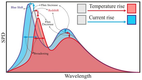
The TSOPs are unique for each electrical working condition, and light output changes depending on the internal quantum efficiency and band gap characteristics of an LED at each specific temperature and input current [
69]. A summarized illustration of the SPD response to temperature and input current induced changes of an arbitrary white LED (WLED) is shown in
Figure 2.
Figure 2. An illustration of temperature and input current induced changes in spectral power distribution (SPD) for an arbitrary WLED. At high temperatures, shown by the gray to red color transition in the figure, radiant flux reduction due to thermal droop, a red shift in dominant wavelengths of chip and phosphor, and full width at half maximum (FWHM) broadening are expected. At higher input current, shown in grey to blue color transition, an increase in power output, blue shift, and broadening at the chip’s FWHM can be seen.
It is known that with increasing
Tj, SPD shows a red shift and broadening [
70]. The redshift phenomenon is primarily due to the band gap reduction. This was explained by Wang et al. [
71,
72] for GaN-based blue LEDs in low temperatures, and recently, similar results were reported at high temperatures for high brightness GaN on sapphire blue LEDs [
73]. It should be noted that SPD displays a blue shift and broadening with increasing input current. Li et al. [
74] studied the effect of input current and temperature on the spectral behavior of green InGaN/GaN multi-quantum well LED and showed that the excitation source could alter the carrier dynamics in the active region. A large blue shift was observed in high input power levels, mainly due to the carrier screening effect as a result of a weakened piezoelectric field that causes the quantum-confined Stark effect [
75]. This issue can be verified by the findings of Kim et al. [
76], which analyzed carrier leakage of GaN based on photoluminescence properties of LEDs both at forward biased and intentionally formed leakage path conditions. Increased current leakages were observed in low series resistance for LEDs, which led to a blue shift of the SPD.
Temperature-induced full width at half maximum (FWHM) broadening is due to the thermal broadening [
77]. On the other hand, current-induced FWHM broadening is due to the combined effect of the screening to the piezoelectric field and band filling effect as discussed by Lin et al. [
70]. With input currents of 150 to 850 mA for GaN-based blue LED at temperature range of 273 to 338 K, the slope of the center of mass wavelength per
Tj was below 0.034 nm/K, while for FWHM, broadening was above 0.052 nm/K. Assuming high precision temperature measurements by taking precise optical measurements within 0.1 nm, the accuracy of the
Tj measurement based on wavelength shift was around 3 K, while the FWHM measurement could reach below 2 K. Based on this, we suggest that FWHM calibration can yield high accuracy in
Tj evaluation.
It should be noted that the spectral width and shape of the LED emission can also be associated with carrier distribution, growth procedure and structure, the density of states, and the successful pairing of electrons and holes, etc. [
78]. For instance, an inconsistent temperature-dependent shifting behavior in wavelength (red–blue–red shifting) was observed for the peak energy of an InGaN based MQW LED and mainly attributed to the non-uniformity (variation in layer thickness and defects) and carrier localization in quantum wells [
79]. Considering these issues, the accuracy of the wavelength shift method is stated to be only 5–10% of the FWHM of the emission line [
80]. However, in devices with a narrow emission, the accuracy of the wavelength shift method increases and can be a suitable approach for
Tj prediction [
81].
Chhajed et al. [
77] calibrated the peak wavelength of ultraviolet (UV), blue, green, and red GaN-based LEDs for a forward current range of 10 to 100 mA at temperatures of 22 to 120 °C. Similarly, a high temperature coefficient of the spectral widths was determined in comparison to the wavelength shift. Temperature coefficients of the dominant wavelength for the blue, green, and red LEDs were determined as 0.0389, 0.0308, and 0.1562 nm/K, respectively. The slopes increase to 0.0466, 0.0625, and 0.1812 nm/K for the FWHM-based
Tj evaluations. Similarly, a strong red shift of the red AlGaInP LED was also seen in another study by the authors for a trichromatic white LED system [
82]. Blueshift was negligible for the red LED and slightly higher for the UV LED, while the highest blueshift effect was recorded for the green LED. The authors stated that the uncertainty of
Tj estimation based on the wavelength shift method is higher in comparison to the FWHM method. Furthermore, the authors preferred the forward voltage method (FVM) with a reported accuracy of ±3 °C over the TSOP method.
Chen et al. [
83] conducted
Tj estimation experiments and obtained peak wavelength shifts for three different AlGaInP LED arrays. Shifting characteristics investigated at longer, central, and shorter wavelengths showed that the center wavelength is the most suitable method to calculate
Tj of an LED array. Tamura et al. [
84] analyzed the wavelength shift of InGaN-based white LEDs at temperatures from 20 to 160 °C and their investigations showed that blue light emission from the active layer and yellow light emission from Ce:YAG phosphor formed two different electroluminescence bands while each band displayed a distinct behavior with the temperature change. However, similar to previous cases,
Tj was stated to be successfully calibrated to the blue emission of the chip. Chen et al. [
85] showed a simplified peak wavelength shift variation at different
Tj for white LEDs under different drive currents. Their findings showed that the temperature dependence of peak wavelength is lower for direct current (DC) LEDs compared to bilevel drive, while the thermal energy needed for correlated color temperature (CCT) stabilization is also less for a DC LED. Gu et al. [
86] selected the point of interest as the lowest energy in the SPD between the peaks of blue and yellow emissions. The ratio of the total radiant energy of white LEDs to the radiant energy within the blue emission in a different
Tj has shown a linear relationship. The authors claimed that with a ratio of 0.005, the temperature prediction accuracy of 1 K can be achieved in commercial white LEDs with this relation. In constant forward current density, Azarifar et al. [
87] performed four machine learning regressions including k-nearest neighbor (KNN), radius near neighbors (RNN), random forest (RF), and extreme gradient booster (XGB) on temperature sensitive optical data from over 500 commercial white LED packages and tested the accuracy of prediction with experimental measurements. With near unity in R
2 scores and small root mean square deviation values, the XGB regressor showed close-to-perfect correlation capability to assess
Tj based on SPD behavior. Their recent findings demonstrated that white LED brightness and color characteristics, irrespective of the package’s thermal resistance, can offer a real-time
Tj prediction capability.
TSOP-based methods have also been shown to be a practical approach for measuring phosphor temperature in an operating white LED. Based on the total emission division of a white LED to a sum of the spectrum of the blue chip and two spectrums from phosphor with a short and a long wavelength band, Yang et al. [
88] examined the fitting peak wavelengths and FWHMs of the short and long wavelength bands at the different phosphor temperatures. They stated that phosphor temperature can be precisely measured by checking the variations of its related emission spectrum. Similar to the LEDs, redshift at higher temperatures was observed. Linear relationships were seen for the FWHM and peak wavelength of the phosphor at different temperatures. However, this model is practical for the same phosphor only, and it cannot be used for mixtures of different phosphor combinations.
Recently, TSOP-based temperature measurement methods have extended to two-dimensional (2D) thermal mapping. Based on new microscopic hyperspectral imaging (MHI), the 2D spectral power distribution can be obtained from light emitting surfaces and can be used to incorporate the TSOP for surface temperature measurement of the LEDs. Jin et al. [
89] used the MHI-based centroid wavelength method to study the 2D temperature distribution of the blue, green, and red LEDs. After calibration of the centroid wavelength coefficient, the authors reached as low as 3 μm resolution for the surface temperature measurement of the LEDs, which is claimed to be capable of reaching submicron level accuracy.
As the next generation micro-LEDs are gaining popularity [
90], practices for performance characterization of micro-LEDs are also becoming a topic of interest. Although previous discussions suggest that heat accumulation in micro-LEDs is lower due to enhanced current spreading in active layers with size reduction [
91], the studies of Feng et al. [
92] and Yu et al. [
93] emphasized the importance of
Tj for micro-LEDs by stating that the internal series resistance of micro-LEDs is expected to increase with their decreasing size. Therefore, it is important to extend the practical application of TSOP-based temperature measurement to the next generation micro-LED devices. Recently, a thermal study on GaN-based micro-LEDs was conducted by Feng et al. [
92]. In their study, a band gap reduction-related redshift of 0.024 eV and FWHM broadening from 27 to 35 nm were seen in the temperature range of 25 to 80 °C. Although they proposed that micro-LED band gap behavior with
Tj follows a semi-empirical Varshni relation, it is not possible to determine an accurate coefficient of temperature for the FWHM or band gap for
Tj calibration from the presented experimental results.
A parametric summary of TSOP-based experimental LED Tj measurement reports is presented in Table 1.
Table 1. TSOP-based experimental temperature measurement parameters that are employed in the literature for the thermal characterization of LEDs. References are sorted by year. Not reported parameters are indicated by a hyphen in the table. (Δδ: uncertainty, λ: wavelength).
This entry is adapted from the peer-reviewed paper 10.3390/mi13101615