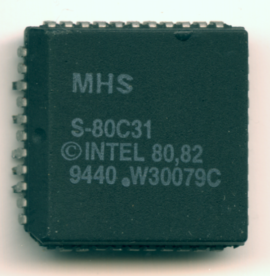
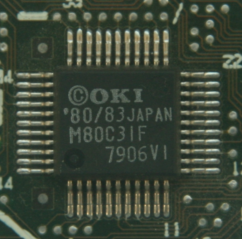
The Intel MCS-51 (commonly termed 8051) is a single chip microcontroller (MCU) series developed by Intel in 1980 for use in embedded systems. The architect of the Intel MCS-51 instruction set was John H. Wharton. Intel's original versions were popular in the 1980s and early 1990s and enhanced binary compatible derivatives remain popular today. It is an example of a complex instruction set computer, and has separate memory spaces for program instructions and data. Intel's original MCS-51 family was developed using N-type metal-oxide-semiconductor (NMOS) technology like its predecessor Intel MCS-48, but later versions, identified by a letter C in their name (e.g., 80C51) use complementary metal–oxide–semiconductor (CMOS) technology and consume less power than their NMOS predecessors. This made them more suitable for battery-powered devices. The family was continued in 1996 with the enhanced 8-bit MCS-151 and the 8/16/32-bit MCS-251 family of binary compatible microcontrollers. While Intel no longer manufactures the MCS-51, MCS-151 and MCS-251 family, enhanced binary compatible derivatives made by numerous vendors remain popular today. Some derivatives integrate a digital signal processor (DSP). Beyond these physical devices, several companies also offer MCS-51 derivatives as IP cores for use in field-programmable gate array (FPGA) or application-specific integrated circuit (ASIC) designs.
- digital signal processor
- single chip
- integrated circuit
1. Important Features and Applications
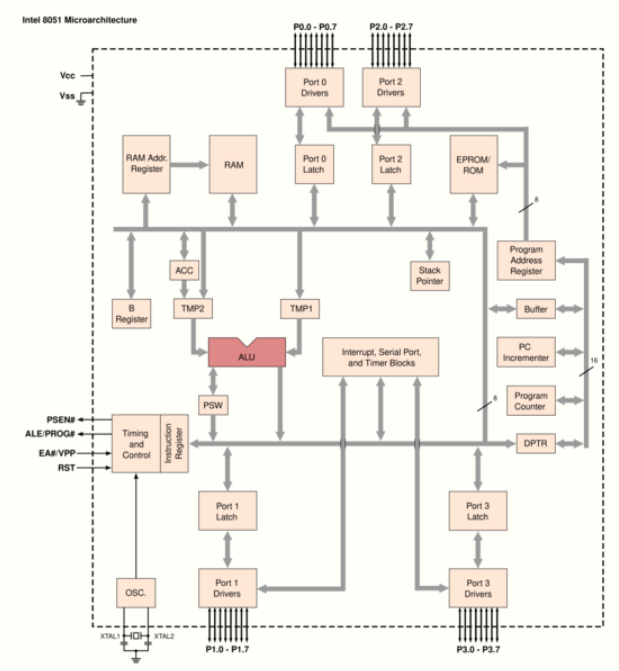
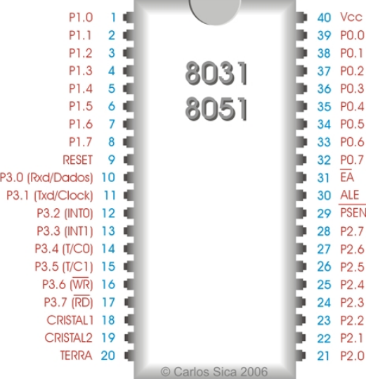
The 8051 architecture provides many functions (central processing unit (CPU), random access memory (RAM), read-only memory (ROM), input/output (I/O) ports, serial port, interrupt control, timers) in one package:
- 8-bit arithmetic logic unit (ALU) and accumulator, 8-bit registers (one 16-bit register with special move instructions), 8-bit data bus and 2×16-bit address buses, program counter, data pointer, and related 8/11/16-bit operations; hence it is mainly an 8-bit microcontroller
- Boolean processor with 17 instructions, 1-bit accumulator, 32 registers (4 bit-addressable 8-bit) and up to 144 special 1 bit-addressable RAM variables (18 bit-addressable 8-bit)[1]
- Multiply, divide and compare instructions
- Four fast switchable register banks with eight registers each (memory mapped)
- Fast interrupt with optional register bank switching
- Interrupts and threads with selectable priority[2]
- 128 or 256 bytes of on-chip RAM (IRAM)
- Dual 16-bit address bus; it can access 2×216 memory locations: 64 KB (65,536 locations) each of ROM (PMEM) and external RAM (XRAM)
- On-chip ROM (not included on 803x variants)
- Four 8-bit bi-directional input/output ports, bit addressable
- UART (serial port)
- Two 16-bit counter/timers
- Power saving mode (on some derivatives)
One feature of the 8051 core is the inclusion of a boolean processing engine, which allows bit-level boolean logic operations to be carried out directly and efficiently on select internal registers, ports and select RAM locations. Another feature is the inclusion of four bank selectable working register sets, which greatly reduce the time required to perform the context switches to enter and leave interrupt service routines. With one instruction, the 8051 can switch register banks, avoiding the time-consuming task of transferring the critical registers to RAM.
Once a UART, and a timer if necessary, has been configured, the programmer needs only write a simple interrupt routine to refill the send shift register whenever the last bit is shifted out by the UART and/or empty the full receive shift register (copy the data somewhere else). The main program then performs serial reads and writes simply by reading and writing 8-bit data to stacks.
1.1. Derivative Features
New derivatives are still being developed by many major chipmakers, and major compiler suppliers such as IAR Systems, Keil and Altium Tasking[3] continuously release updates.
MCS-51 based microcontrollers typically include one or two UARTs, two or three timers, 128 or 256 bytes of internal data RAM (16 bytes of which are bit-addressable), up to 128 bytes of I/O, 512 bytes to 64 KB of internal program memory, and sometimes a quantity of extended data RAM (ERAM) located in the external data space. External RAM and ROM share the data and address buses. The original 8051 core ran at 12 clock cycles per machine cycle, with most instructions executing in one or two machine cycles. With a 12 MHz clock frequency, the 8051 could thus execute 1 million one-cycle instructions per second or 500,000 two-cycle instructions per second. Enhanced 8051 cores are now commonly used which run at six, four, two, or even one clock per machine cycle, and have clock frequencies of up to 100 MHz, and are thus capable of an even greater number of instructions per second. All Silicon Labs, some Dallas and a few Atmel devices have single cycle cores.
8051 variants may include built-in reset timers with brown-out detection, on-chip oscillators, self-programmable flash ROM program memory, built-in external RAM, extra internal program storage, bootloader code in ROM, EEPROM non-volatile data storage, I²C, SPI, and USB host interfaces, CAN or LIN bus, ZigBee or Bluetooth radio modules, PWM generators, analog comparators, analog-to-digital and digital-to-analog converters, RTCs, extra counters and timers, in-circuit debugging facilities, more interrupt sources, extra power saving modes, more/less parallel ports etc. Intel manufactured a mask programmed version, 8052AH-BASIC, with a BASIC interpreter in ROM, capable of running user programs loaded into RAM.
MCS-51 based microcontrollers have been adapted to extreme environments. Examples for high-temperature variants are the Tekmos TK8H51 family for −40 °C to +250 °C[4] or the Honeywell HT83C51 for −55 °C to +225 °C (with operation for up to 1 year at +300 °C).[5] Radiation-hardenend MCS-51 microcontrollers for use in spacecraft are available; e.g., from Cobham (formerly Aeroflex) as the UT69RH051[6] or from NIIET as the 1830VE32 (Russian: 1830ВЕ32).[7]
In some engineering schools, the 8051 microcontroller is used in introductory microcontroller courses.[8][9][10][11]
2. Family Naming Conventions
8051 is the original name by Intel with 4 KB ROM and 128 byte RAM. Variants starting with 87 have a user programmable EPROM, sometimes UV erasable. Variants with a C as the third character are some kind of CMOS. 8031 and 8032 are ROM-less versions, with 128 and 256 bytes RAM. The last digit can indicate memory size, e.g. 8052 with 8 KB ROM, 87C54 16 KB EPROM, and 87C58 with 32 KB EPROM, all with 256 byte RAM.
3. Memory Architecture
The MCS-51 has four distinct types of memory: internal RAM, special function registers, program memory, and external data memory.
The 8051 is designed as a modified Von-Neumann Architecture with segregated memory (data and instructions); it can only execute code fetched from program memory, and has no instructions to write to program memory. Which is similar to Harvard Architecture.
Most 8051 systems respect this distinction, and so are unable to download and directly execute new programs. Although the 8051's architecture is unique; the buses to access both types of memory are the same; only the data bus, the address bus, and the control bus leave the processor.
3.1. Internal RAM
Internal RAM (IRAM) has an 8-bit address space, using addresses 0 through 0xFF. IRAM from 0x00 to 0x7F can be accessed directly, using an 8-bit absolute address that is part of the instruction. Alternatively, IRAM can be accessed indirectly: the address is loaded into R0 or R1, and the memory is accessed using the @R0 or @R1 syntax.
The original 8051 has only 128 bytes of IRAM. The 8052 added IRAM from 0x80 to 0xFF, which can only be accessed indirectly; direct access to this address range goes to the special function registers. Most 8051 clones also have a full 256 bytes of IRAM.
The 32 bytes from 0x00–0x1F memory-map the 8 registers R0–R7. Eight bytes are used at a time; two program status word bits select between four possible banks.
The 16 bytes (128 bits) at IRAM locations 0x20–0x2F are bit-addressable.
3.2. Special Function Registers
Special function registers (SFR) are located in the same address space as IRAM, at addresses 0x80 to 0xFF, and are accessed directly using the same instructions as for the lower half of IRAM. They cannot be accessed indirectly via @R0 or @R1; indirect access to those addresses will access the second half of IRAM.
Sixteen of the SFRs (those whose addresses are multiples of 8) are also bit-addressable.
3.3. Program Memory
Program memory (PMEM, though less common in usage than IRAM and XRAM) is up to 64 KB of read-only memory, starting at address 0 in a separate address space. It may be on- or off-chip, depending on the particular model of chip being used. Program memory is read-only, though some variants of the 8051 use on-chip flash memory and provide a method of re-programming the memory in-system or in-application.
In addition to code, it is possible to store read-only data such as lookup tables in program memory, retrieved by the MOVC A,@A+DPTR or MOVC A,@A+PC instructions. The address is computed as the sum of the 8-bit accumulator and a 16-bit register (PC or DPTR).
Special jump and call instructions (AJMP and ACALL) slightly reduce the size of code that accesses local (within the same 2 KB) program memory.[12]
3.4. External Data Memory
External data memory (XRAM) is a third address space, also starting at address 0, and allowing 16 bits of address space. It can also be on- or off-chip; what makes it "external" is that it must be accessed using the MOVX (move external) instruction. Many variants of the 8051 include the standard 256 bytes of IRAM plus a few kilobytes of XRAM on the chip.
The first 256 bytes of XRAM may be accessed using the MOVX A,@R0, MOVX A,@R1, MOVX @R0,A, and MOVX @R1,A instructions. The full 64KB may be accessed using MOVX A,@DPTR and MOVX @DPTR,A.
4. Registers
The only register on an 8051 that is not memory-mapped is the 16-bit program counter (PC). This specifies the address of the next instruction to execute. Relative branch instructions supply an 8-bit signed offset which is added to the PC.
Eight general-purpose registers R0–R7 may be accessed with instructions one byte shorter than others. They are mapped to IRAM between 0x00 and 0x1F. Only eight bytes of that range are used at any given time, determined by the two bank select bits in the PSW.
The following is a partial list of the 8051's registers, which are memory-mapped into the special function register space:
- Stack pointer, SP (0x81)
- This is an 8-bit register used by subroutine call and return instructions. The stack grows upward; the SP is incremented before pushing, and decremented after popping a value.
- Data pointer, DP (0x82–83)
- This is a 16-bit register that is used for accessing PMEM and XRAM.
- Program status word, PSW (0xD0)
- This contains important status flags, by bit number:
- Parity, P. Gives the parity (XOR of the bits) of the accumulator, A.
- User defined, UD. May be read and written by software; not otherwise affected by hardware.
- Overflow flag, OV. Set when addition produces a signed overflow.
- Register select 0, RS0. The low-order bit of the register bank. Set when banks at 0x08 or 0x18 are in use.
- Register select 1, RS1. The high-order bit of the register bank. Set when banks at 0x10 or 0x18 are in use.
- Flag 0, F0. May be read and written by software; not otherwise affected by hardware.
- Auxiliary carry, AC. Set when addition produces a carry from bit 3 to bit 4.
- Carry bit, C. Often used as the general register for bit computations, or the "Boolean accumulator".
- Accumulator, A (0xE0)
- This register is used by most instructions.
- B register (0xF0)
- This is used as an extension to the accumulator for multiply and divide instructions.
256 single bits are directly addressable. These are the 16 IRAM locations from 0x20–0x2F, and the 16 special function registers 0x80, 0x88, 0x90, ..., 0xF8. Any bit of these bytes may be directly accessed by a variety of logical operations and conditional branches.
Note that the PSW does not contain the common negative (N), or zero (Z) flags. For the former, the most significant bit of the accumulator can be addressed directly, as it is a bit-addressable SFR. For the latter, there are explicit instructions to jump on whether or not the accumulator is zero. There is also a two-operand compare and jump operation.
5. Instruction Set
Instructions are all 1 to 3 bytes long, consisting of an initial opcode byte, followed by up to 2 bytes of operands.
1⁄4 of the opcode bytes, x0–x3, are used for irregular opcodes.
3⁄4 of the opcode bytes, x4–xF, are assigned to 16 basic ALU instructions with 12 possible operands. The least significant nibble of the opcode selects the primary operand as follows:
- x8–xF: Register direct, R0–R7.
- x6–x7: Register indirect, @R0 or @R1.
- x5: Memory direct, a following byte specifies an IRAM or SFR location.
- x4: Immediate, a following byte specifies an 8-bit constant. When the operand is a destination (
INC operand,DEC operand) or the operation already includes an immediate source (MOV operand,#data,CJNE operand,#data,offset), this instead specifies that the accumulator is used.
The most significant nibble specifies the operation as follows. Not all support all addressing modes; the immediate mode in particular is unavailable when the primary operand is written to. Instruction mnemonics use destination, source operand order.
- 0y:
INC operand - Increment the specified operand. Immediate mode (opcode 0x04) specifies the accumulator,
INC A. - 1y:
DEC operand - Decrement the specified operand. Immediate mode (opcode 0x14) specifies the accumulator,
DEC A. - 2y:
ADD A,operand - Add the operand to the accumulator, A. Opcode 0x23 (
RL A, "rotate left" but actually a shift left) may be thought of asADD A,A. - 3y:
ADDC A,operand - Add the operand, plus the C bit, to the accumulator. Opcode 0x33 (
RLC A, rotate left through carry) may be thought of asADDC A,A. - 4y:
ORL A,operand - Logical OR the operand into the accumulator. Two memory-destination forms of this operation,
ORL address,#dataandORL address,A, are specified by opcodes 0x43 and 0x42. - 5y:
ANL A,operand - Logical AND the operand into the accumulator. Two memory-destination forms of this operation,
ANL address,#dataandANL address,A, are specified by opcodes 0x53 and 0x52. - 6y:
XRL A,operand - Logical exclusive-OR the operand into the accumulator. Two memory-destination forms of this operation,
XRL address,#dataandXRL address,A, are specified by opcodes 0x63 and 0x62. - 7y:
MOV operand,#data - Move immediate to the operand. Immediate mode (opcode 0x74) specifies the accumulator,
MOV A,#data. - 8y:
MOV address,operand - Move value to an IRAM or SFR register. Immediate mode (opcode 0x84) is not used for this operation, as it duplicates opcode 0x75.
- 9y:
SUBB A,operand - Subtract the operand from the accumulator. This operation borrows and there is no subtract without borrow.
- Ay:
MOV operand,address - Move value from an IRAM or SFR register. Immediate mode (opcode 0xA4) is not used, as immediates serve only as sources. Memory direct mode (opcode 0xA5) is not used, as it duplicates 0x85.
- By:
CJNE operand,#data,offset - Compare operand to the immediate
#data, and jump to PC + offset if not equal. Immediate and memory direct modes (opcodes 0xB4 and 0xB5) compare the operand against the accumulator,CJNE A,operand,offset. Note that there is no compare and jump if equal instruction,CJE. - Cy:
XCH A,operand - Exchange the accumulator and the operand. Immediate mode (opcode 0xC4) is not used for this operation.
- Dy:
DJNZ operand,offset - Decrement the operand, and jump to PC + offset if the result is non-zero. Immediate mode (opcode 0xD4), and register indirect mode (0xD6, 0xD7) are not used.
- Ey:
MOV A,operand - Move operand to the accumulator. Immediate mode is not used for this operation (opcode 0xE4), as is duplicates opcode 0x74.
- Fy:
MOV operand,A - Move accumulator to the operand. Immediate mode (opcode 0xF4) is not used, as it would have no effect.
Only the ADD, ADDC, and SUBB instructions set PSW flags. The INC, DEC, and logical instructions do not. The CJNE instruction modifies the C bit only, to the borrow that results from operand1 − operand2.
The irregular instructions comprise 64 opcodes, having more limited addressing modes, plus several opcodes scavenged from inapplicable modes in the regular instructions.
| Opcode | x0 | x1 | x2 | x3 | x4 |
|---|---|---|---|---|---|
| 0y | NOP |
|
LJMP addr16 |
RR A (rotate right) |
INC A |
| 1y | JBC bit,offset (jump if bit set with clear) |
LCALL addr16 |
RRC A (rotate right through carry) |
DEC A |
|
| 2y | JB bit,offset (jump if bit set) |
RET |
RL A (rotate left) |
ADD A,#data |
|
| 3y | JNB bit,offset (jump if bit clear) |
RETI |
RLC A (rotate left through carry) |
ADDC A,#data |
|
| 4y | JC offset (jump if carry set) |
ORL address,A |
ORL address,#data |
ORL A,#data |
|
| 5y | JNC offset (jump if carry clear) |
ANL address,A |
ANL address,#data |
ANL A,#data |
|
| 6y | JZ offset (jump if zero) |
XRL address,A |
XRL address,#data |
XRL A,#data |
|
| 7y | JNZ offset (jump if non-zero) |
ORL C,bit |
JMP @A+DPTR |
MOV A,#data |
|
| 8y | SJMP offset (short jump) |
ANL C,bit |
MOVC A,@A+PC |
DIV AB |
|
| 9y | MOV DPTR,#data16 |
MOV bit,C |
MOVC A,@A+DPTR |
SUBB A,#data |
|
| Ay | ORL C,/bit |
MOV C,bit |
INC DPTR |
MUL AB |
|
| By | ANL C,/bit |
CPL bit |
CPL C |
CJNE A,#data,offset |
|
| Cy | PUSH address |
CLR bit |
CLR C |
SWAP A |
|
| Dy | POP address |
SETB bit |
SETB C |
DA A (decimal adjust) |
|
| Ey | MOVX A,@DPTR |
MOVX A,@R0 |
MOVX A,@R1 |
CLR A |
|
| Fy | MOVX @DPTR,A |
MOVX @R0,A |
MOVX @R1,A |
CPL A |
- A5
- Unused
- B5
CJNE A,address,offset- D6–7
XCHD A,@R0–1exchange low-order nibble of operands.
The SJMP (short jump) opcode takes a signed relative offset byte operand and transfers control there relative to the address of the following instruction. The AJMP/ACALL opcodes combine the three most significant bits of the opcode byte with the following byte to specify an 11-bit destination that is used to replace 11 bottom bits of the PC register (top 5 bits of PC register remain intact). For larger addresses, the LJMP and LCALL instructions allow a 16-bit destination.
One of the reasons for the 8051's popularity is its range of operations on single bits. Bits are always specified by absolute addresses; there is no register-indirect or indexed addressing. Instructions that operate on single bits are:
SETB bit,CLR bit,CPL bit: Set, clear, or complement the specified bitJB bit,offset: Jump if bit setJNB bit,offset: Jump if bit clearJBC bit,offset: Jump if bit set, and clear bitMOV C,bit,MOV bit,C: Move the specified bit to the carry bit, or vice versaORL C,bit,ORL C,/bit: Or the bit (or its complement) to the carry bitANL C,bit,ANL C,/bit: And the bit (or its complement) to the carry bit
A bit operand is written in the form address.number. Because the carry flag is bit 7 of the bit-addressable program status word, the SETB C, CLR C and CPL C instructions are shorter equivalents to SETB PSW.7, CLR PSW.7 and CPL PSW.7.
Although most instructions require that one operand is the accumulator or an immediate constant, opcode 0x85 performs MOV directly between two internal RAM locations.
6. Programming
There are various high-level programming language compilers for the 8051. Several C compilers are available for the 8051, most of which allow the programmer to specify where each variable should be stored in its six types of memory, and provide access to 8051 specific hardware features such as the multiple register banks and bit manipulation instructions. There are many commercial C compilers.[13] Small Device C Compiler (SDCC) is a popular open source C compiler.[14] Other high level languages such as C++, Forth,[15][16][17][18] BASIC, Object Pascal, Pascal, PL/M and Modula-2 are available for the 8051, but they are less widely used than C and assembly.
Because IRAM, XRAM, and PMEM (read only) all have an address 0, C compilers for the 8051 architecture provide compiler-specific pragmas or other extensions to indicate where a particular piece of data should be stored (i.e. constants in PMEM or variables needing fast access in IRAM). Since data could be in one of three memory spaces, a mechanism is usually provided to allow determining to which memory a pointer refers, either by constraining the pointer type to include the memory space, or by storing metadata with the pointer.
7. Related Processors
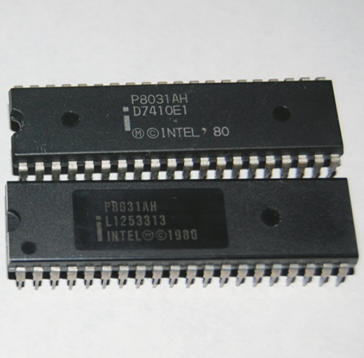
Intel discontinued its MCS-51 product line in March 2007;[19][20] however, there are plenty of enhanced 8051 products or silicon intellectual property added regularly from other vendors.
The 8051's predecessor, the 8048, was used in the keyboard of the first IBM PC, where it converted keypresses into the serial data stream which is sent to the main unit of the computer. An Intel 8049 served a similar role in the Sinclair QL. The 8048 and derivatives are still used (As of 2007) for basic model keyboards.
The 8031 was a reduced version of the original 8051 that had no internal program memory (read-only memory, ROM). To use this chip, external ROM had to be added containing the program that the 8031 would fetch and execute. An 8051 chip could be sold as a ROM-less 8031, as the 8051's internal ROM is disabled by the normal state of the EA pin in an 8031-based design. A vendor might sell an 8051 as an 8031 for any number of reasons, such as faulty code in the 8051's ROM, or simply an oversupply of 8051s and undersupply of 8031s.
The 8052 was an enhanced version of the original 8051 that featured 256 bytes of internal RAM instead of 128 bytes, 8 KB of ROM instead of 4 KB, and a third 16-bit timer. Most modern 8051-compatible microcontrollers include these features.
The 8032 had these same features as the 8052 except lacked internal ROM program memory.
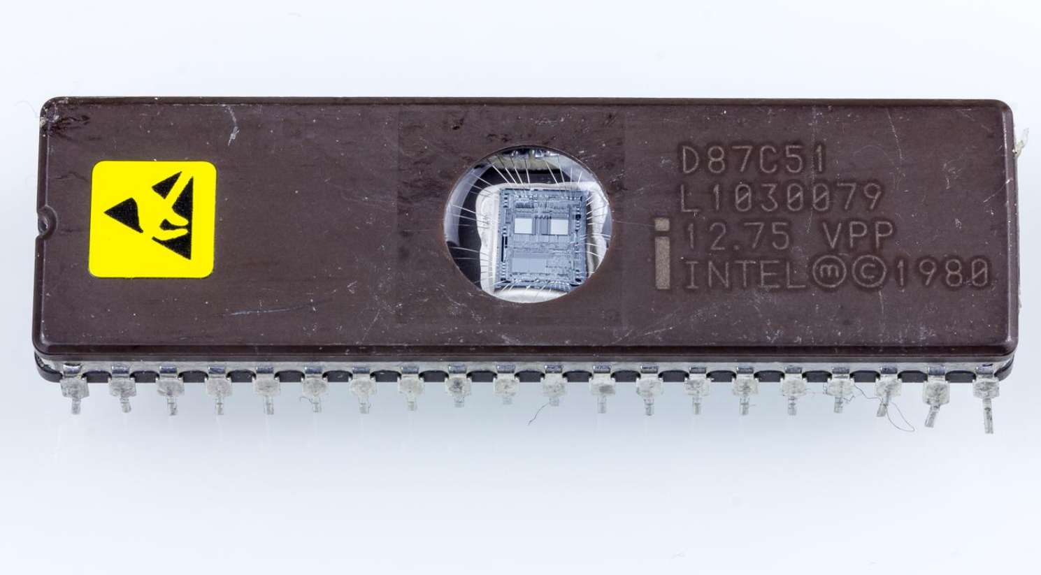
The 8751 was an 8051 with 4 KB EPROM instead of 4 KB ROM. They were identical except for the non-volatile memory type. This part was available in a ceramic package with a clear quartz window over the top of the die so UV light could be used to erase the EPROM. Related parts are: 8752 had 8 KB EPROM, 8754 had 16 KB EPROM, 8758 had 32 KB EPROM.
The 80C537 (ROM-less) and 80C517 (8 KB ROM) are CMOS versions, designed for the Automotive industry . Enhancements mostly include new and enhanced peripherals. The 80C5x7 has fail-safe mechanisms, analog signal processing facilities, enhanced timer capabilities, and a 32-bit arithmetic peripheral. Other features include:
- 256 byte on-chip RAM
- 256 directly addressable bits
- External program and data memory expandable up to 64 KB
- 8-bit A/D converter with 12 multiplexed inputs
- Arithmetic peripheral can perform 16×16→32-bit multiplication, 32/16→16-bit division, 32-bit shift and 32-bit normalize operations
- Eight data pointers instead of one for indirect addressing of program and external data memory
- Extended watchdog facilities
- Nine I/O ports
- Two full-duplex serial interfaces with individual baud rate generators
- Four priority level interrupt systems, 14 interrupt vectors
- Three power saving modes
Intel MCS-51 second sources

AMD P8031. https://handwiki.org/wiki/index.php?curid=1605545
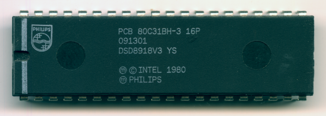
Philips PCB80C31. https://handwiki.org/wiki/index.php?curid=1890941

Signetics SCN8031. https://handwiki.org/wiki/index.php?curid=1183546
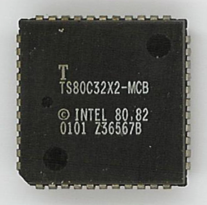
Temic TS80C32. https://handwiki.org/wiki/index.php?curid=1282512
7.1. Derivative Vendors
More than 20 independent manufacturers produce MCS-51 compatible processors.
Intel MCS-51 derived microcontrollers
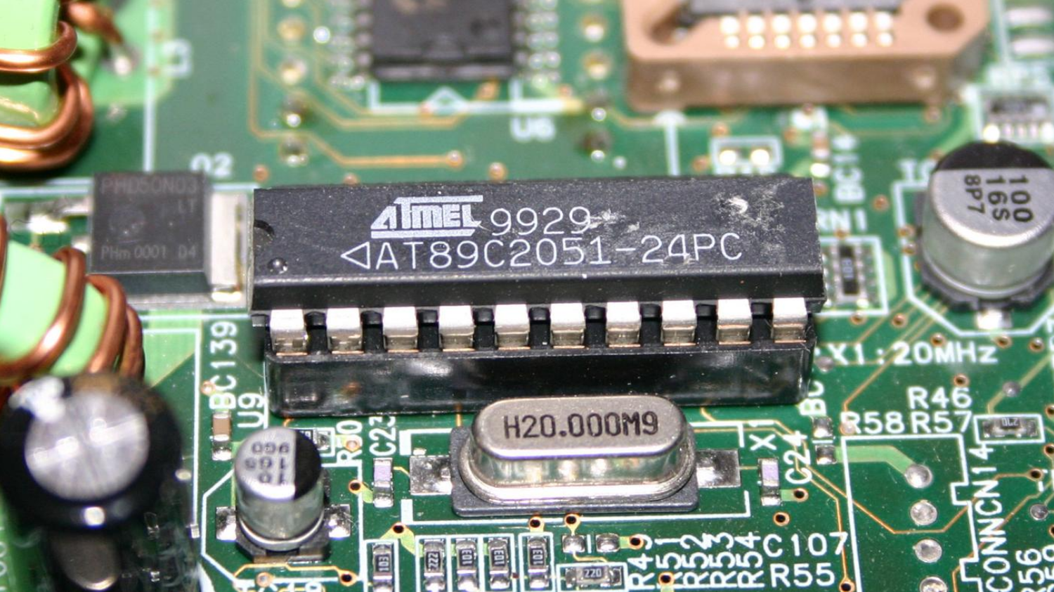
Atmel AT89C2051. https://handwiki.org/wiki/index.php?curid=1240450
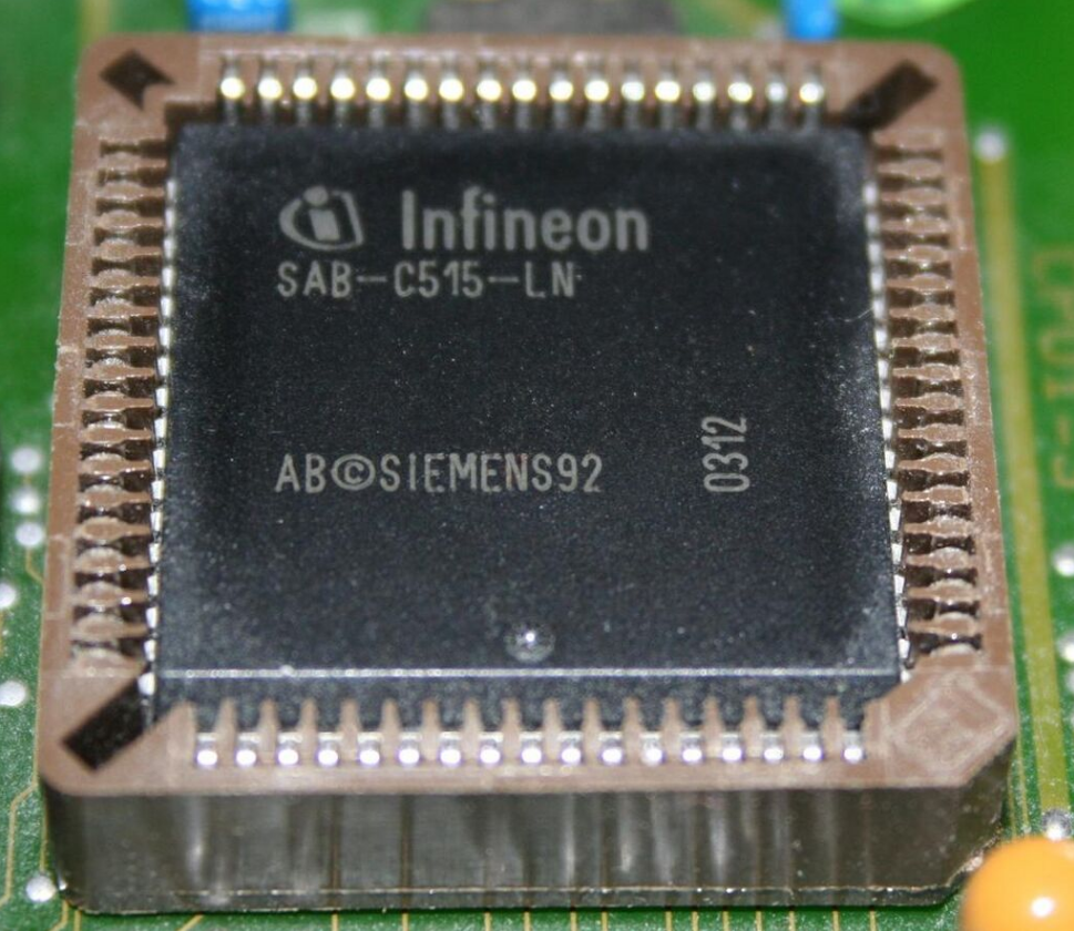
Infineon SAB-C515. https://handwiki.org/wiki/index.php?curid=1794008
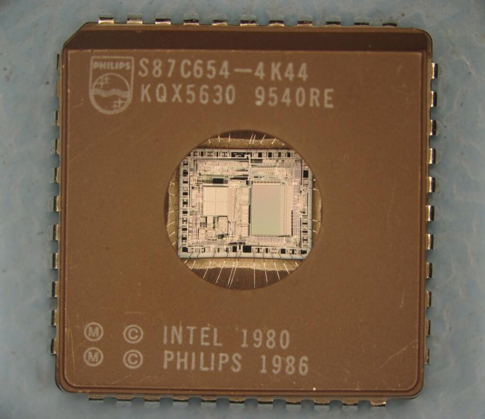
Philips S87C654. https://handwiki.org/wiki/index.php?curid=1592561
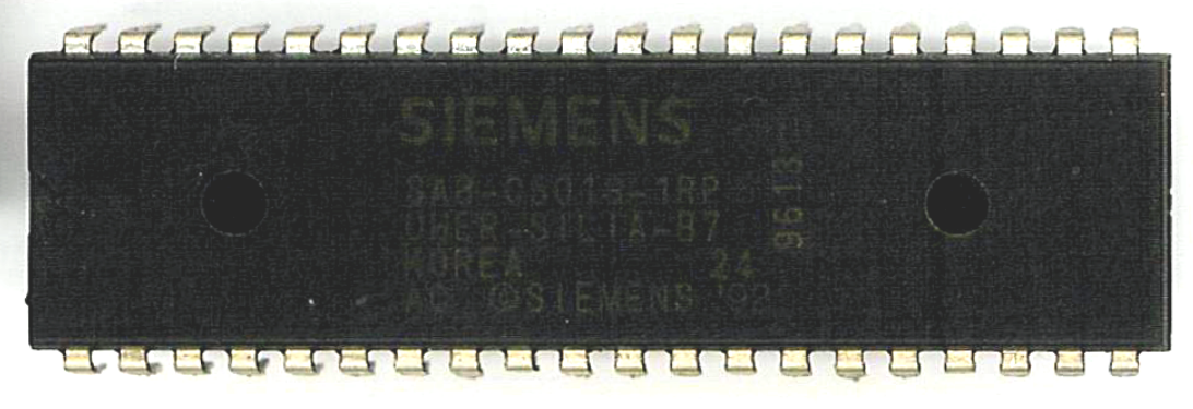
Siemens SAB-C501. https://handwiki.org/wiki/index.php?curid=1768813
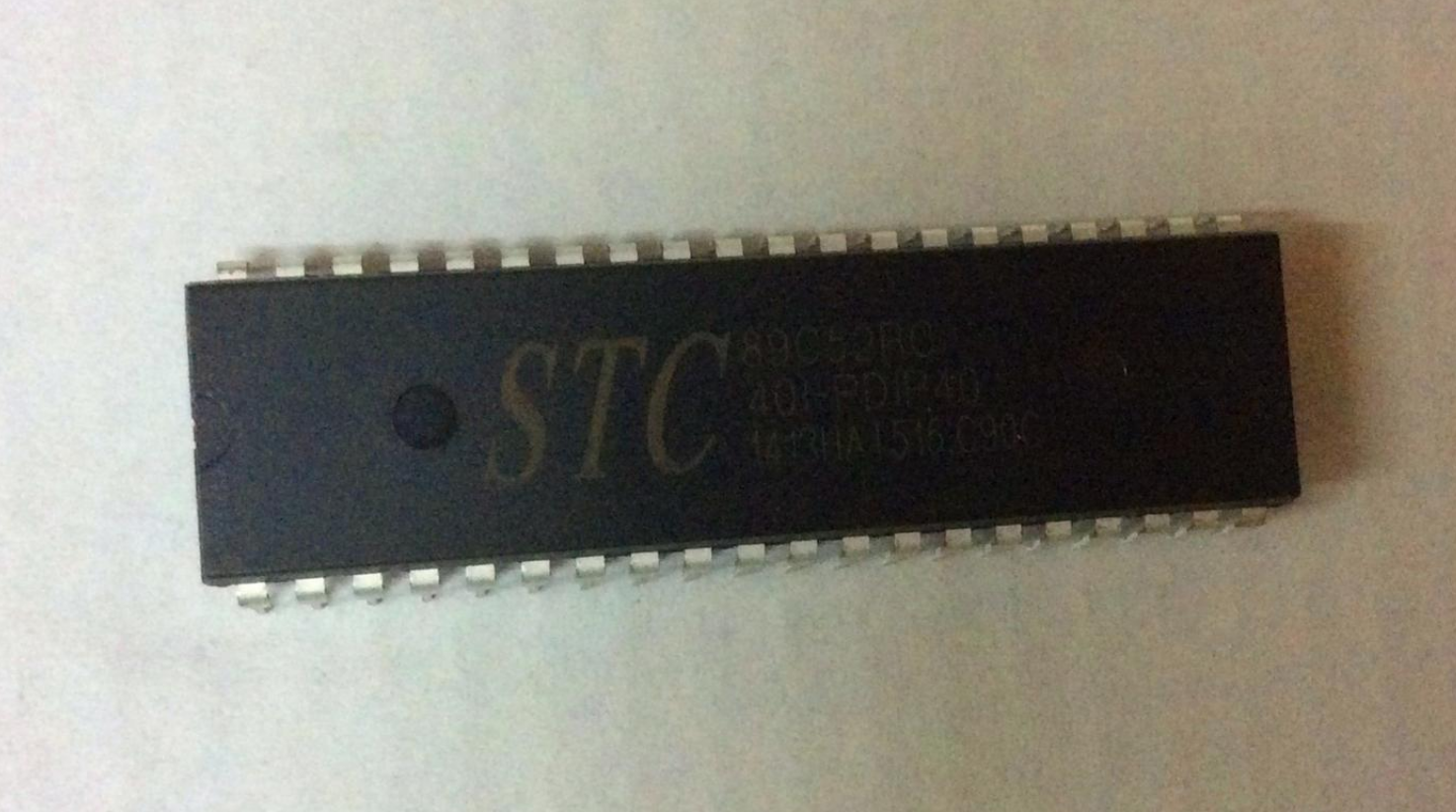
STC Micro STC89C52. https://handwiki.org/wiki/index.php?curid=1900495
Other ICs or IPs compatible with the MCS-51 have been developed by Analog Devices,[21] Integral Minsk,[22] Kristall Kiev,[23] and NIIET Voronesh.[7]
8. Use as Intellectual Property
Today, 8051s are still available as discrete parts, but they are mostly used as silicon intellectual property cores.[24] Available in hardware description language source code (such as VHDL or Verilog) or FPGA netlist forms, these cores are typically integrated within embedded systems, in products ranging from USB flash drives to washing machines to complex wireless communication systems on a chip. Designers use 8051 silicon IP cores, because of the smaller size, and lower power, compared to 32 bit processors like ARM Cortex-M series, MIPS and BA22.
Modern 8051 cores are faster than earlier packaged versions. Design improvements have increased 8051 performance while retaining compatibility with the original MCS 51 instruction set. The original Intel 8051 ran at 12 clock cycles per machine cycle, and most instructions executed in one or two machine cycles. A typical maximum clock frequency of 12 MHz meant these old 8051s could execute one million single-cycle instructions, or 500,000 two-cycle instructions, per second. In contrast, enhanced 8051 silicon IP cores now run at one clock cycle per machine cycle, and have clock frequencies of up to 450 MHz. That means an 8051-compatible processor can now execute 450 million instructions per second.
9. MCUs Based on 8051
- ABOV: MC94F, MC95F, MC96F series
- Atmel: AT89C51, AT89S51, AT83C5134
- Infineon: XC800
- Maxim Integrated: DS89C4 series (DS89C420, DS89C430, DS89C440, DS89C450)
- Mentor Graphics: M8051ew
- Megawin: 74, 82, 84, 86, 87, and 89 series
- NXP: NXP700 and NXP900 series
- Siemens SAB 80532-N
- Silicon Labs: C8051 series and EFM8 series
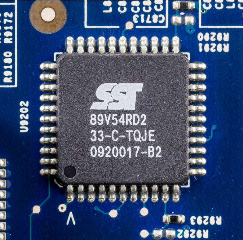
- Silicon Storage Technology: FlashFlex51 MCU (SST89E52RD2, SST89E54RD2, SST89E58RD2, SST89E516RD2SST89V52RD2, SST89V54RD2, SST89V58RD2, SST89V516RD2)[25]
- STC Micro: STC89C51RC, STC90C51RC, STC90C58AD, STC10F08XE, STC11F60XE, STC12C5410AD, STC12C5202AD, STC12C5A60S2, STC12C5628AD, STC15F100, STC15F204EA, STC15F2K60S2, STC15F4K60S2, STC15F101W, STC15F408AD, STC15W104, STC15W408S, STC15W201S, STC15W408AS, STC15W1K16S and STC15W4K56S4 series[26]
- Texas Instruments CC111x, CC24xx and CC25xx families of RF SoCs
- WCH: CH551, CH552, CH554, CH546, CH547, CH548, CH558, CH559
10. Digital Signal Processor (DSP) Variants
Several variants with an additional 16-bit digital signal processor (DSP) (for example for MP3 or Vorbis coding/decoding) with up to 675 million instructions per second (MIPS)[27] and integrated USB 2.0 interface[28] or as intellectual property[29] exist.
11. Enhanced 8-bit Binary Compatible Microcontroller: MCS-151 Family
In 1996 Intel announced the MCS-151 family, an up to 6 times faster variant,[30] that's fully binary and instruction set compatible with 8051. Unlike their 8051 MCS-151 is a pipelined CPU, with 16-bit internal code bus and is 6x the speed. The MCS-151 family was also discontinued by Intel, but is widely available in binary compatible and partly enhanced variants.
12. 8/16/32-bit Binary Compatible Microcontroller: MCS-251 Family
The 80251 8/16/32-bit microcontroller with 16 MB (24-bit) address-space and 6 times faster instruction cycle was introduced by Intel in 1996.[30][31] It can perform as an 8-bit 8051, has 24-bit linear addressing, an 8-bit ALU, 8-bit instructions, 16-bit instructions, a limited set of 32-bit instructions, 16 8-bit registers, 16 16-bit registers (8 16-bit registers which do not share space with any 8-bit registers, and 8 16-bit registers which contain 2 8-bit registers per 16-bit register), and 10 32-bit registers (2 dedicated 32-bit registers, and 8 32-bit registers which contain 2 16-bit registers per 32-bit register).[32]
It features extended instructions[33] – see also the programmer's guide[34] – and later variants with higher performance,[35] also available as intellectual property (IP).[36] It is 3-stage pipelined. The MCS-251 family was also discontinued by Intel, but is widely available in binary compatible and partly enhanced variants from many manufacturers.
The content is sourced from: https://handwiki.org/wiki/Engineering:Intel_MCS-51
References
- John Wharton: Using the Intel MCS-51 Boolean Processing Capabilities Application Note AP-70, May 1980, Intel Corporation. http://www2.elo.utfsm.cl/~lsb/elo311/aplicaciones/intel/booleanproc.pdf
- "8051 Tutorial: Interrupts". http://www.8052.com/tutint.phtml.
- "TASKING". https://www.tasking.com/.
- "TK80H51 250ºC Microcontroller". Tekmos Inc.. http://www.tekmos.com/products/80c51-microcontrollers/tk80h51-250-c-microcontroller. Retrieved 23 August 2017.
- "HIGH TEMPERATURE 83C51 MICROCONTROLLER". Honeywell. http://www.keil.com/dd/docs/datashts/honeywell/ht83c51.pdf. Retrieved 23 August 2017.
- "Microcontrollers and Microprocessors". Cobham Semiconductor Solutions. http://ams.aeroflex.com/pagesproduct/prods-hirel-uprocessors.cfm. Retrieved 23 August 2017.
- "Микроконтроллеры" (in Russian). OAO "NIIET". http://niiet.ru/goods/chips/microcont. Retrieved 22 August 2017.
- "Archived copy". http://play.tojsiab.com/WFhtU3d2djNXckUz.
- https://www.youtube.com/watch?v=H9sDn89EvD8
- "ELEC2700 - Computer Engineering 2 - University of Newcastle - Textbooks | Zookal.com". https://www.zookal.com/.
- http://s3.amazonaws.com/f01.justanswer.com/88willy/2012-06-29_065532_assignment_03.pdf
- ACALL is a 2-byte subroutine calling instruction, it can access locations within the same 2 KB segment of memory. The absolute memory address is formed by the high 5 bits of the PC and the 11 bits defined by the instruction.
- Han-Way Huang. "Embedded System Design with C8051". p. 238. https://books.google.com/books?id=PnXNNGG_jMMC
- Lewin A. R. W. Edwards. "So, You Wanna be an Embedded Engineer: The Guide to Embedded Engineering, from Consultancy to the Corporate Ladder". 2006. p. 51. https://archive.org/details/pdfy-MKFMCCNbqENoR3Ft
- Bradford J. Rodriguez. "CamelForth/8051". http://www.camelforth.com/page.php?4
- Brad Rodriguez. "Moving Forth Part 7: CamelForth for the 8051". http://www.bradrodriguez.com/papers/moving7.htm
- "8051 SwiftX Forth development". http://www.forth.com/embedded/swiftx-embedded-systems-development-tools.html?MCU=8051
- "MPE VFX Forth 7 cross compilers". http://www.mpeforth.com/xc7.htm
- Ganssle, Jack (2006-05-29). "Intel bows out, discontinues MCS-51". http://www.embedded.com/electronics-blogs/break-points/4025678/Intel-bows-out.
- "MCS 51, MCS 251 and MCS 96 Microcontroller Product Lines, the Intel 186, Intel386 and Intel486 Processors Product Lines, and the i960 32 Bit RISC Processor, PCN 106013-01, Product Discontinuance, Reason for Revision: Add Key Milestone information and revise description of change". Intel. 2006-05-02. http://qdms.intel.com/dm/d.aspx/7C715FEC-C598-444E-9EFB-2750B98F7956/PCN106013-01.pdf.
- http://www.analog.com/static/imported-files/data_sheets/ADUC832.pdf
- "Микроконтроллеры и супервизоры питания Серии 1880; 1881; 1842; 588; 1345; 5518АП1ТБМ" (in Russian). OAO "Integral". http://integral.by/ru/products/mikrokontrollery-i-supervizory-pitaniya-serii-1880-1881-1842-588-1345-5518ap1tbm. Retrieved 6 January 2017.
- "Однокристальные микро-эвм" (in Russian). Kristall. http://krystall.net.ua/ru/products/53.html. Retrieved 5 January 2017.
- Hussaini (20 August 2019). "Why do we have to use the 8051? Isn't it too old?". https://www.technobyte.org/8051-not-old-still-popular-use-why/.
- datasheetq.com. "89V54RD2 Datasheet PDF Download - Silicon Storage Technology" (in en). https://www.datasheetq.com/datasheet-download/190246/1/SST/89V54RD2.
- "STC Microcontroller---STCmicro Technology Co,.Ltd". http://www.stcmicro.com/stcmcu.html.
- "TI Delivers new low-cost, high-performance audio DSP for Home and Car w/ 8051". http://www.8052.com/news?NEWSID=61#.
- "Atmel AT85C51SND3 Audio DSP Data Sheet with USB 2.0". http://www.keil.com/dd/docs/datashts/atmel/at85c51snd3.pdf.
- Salim, A.J.; Othman, M.; Ali, M.A. Mohd (October 5, 2006). "Integration of 8051 With DSP in Xilinx FPGA". pp. 562–566. doi:10.1109/SMELEC.2006.380694. https://ieeexplore.ieee.org/document/4266677/?reload=true&tp=&arnumber=4266677&url=http://ieeexplore.ieee.org/iel5/4266544/4266545/04266677.pdf?arnumber=4266677.
- "Intel MCS® 151 and MCS® 251 Microcontrollers". http://datasheets.chipdb.org/Intel/MCS51/151BACK.HTM.
- The 8051 microcontroller By Kenneth J Ayala Google books https://books.google.com/books?id=l6lveWkWqFoC&pg=PA400&lpg=PA400&ots=aX1rfMDJdF&dq=intel+80251&ie=ISO-8859-1&output=html
- http://datasheets.chipdb.org/Intel/MCS51/DATASHTS/27262001.PDF
- "Temic TSC80251 Architecture". http://pe2bz.philpem.me.uk/pdf%20on%20typenumber/A-C/C251.pdf.
- "Atmel TSC80251 Programmers Guide". http://www.cs.unc.edu/~vicci/comp261/project/mcu/80251_prog_man.pdf.
- DQ80251 32bit Microcontroller DCD http://dcd.pl/workspace/documentation/lat/dq80251_ds.pdf
- R80251XC 32bit Microcontroller Evatronix http://www.evatronix.pl/products/pdf/r80251xc_datasheet.pdf

