A Substrate integrated waveguide (SIW) (also known as post-wall waveguide or laminated waveguide) is a synthetic rectangular electromagnetic waveguide formed in a dielectric substrate by densely arraying metallized posts or via-holes which connect the upper and lower metal plates of the substrate. The waveguide can be easily fabricated with low-cost mass-production using through-hole techniques where the post walls consists of via fences. SIW is known to have similar guided wave and mode characteristics to conventional rectangular waveguide with equivalent guide wavelength. Since the emergence of new communication technologies in the 1990s, there has been an increasing need for high-performance millimeter-wave systems. These need to be reliable, low-cost, compact, and compatible with high-frequencies. Unfortunately, above 10 GHz, the well known microstrip and coplanar lines technologies cannot be used because they have high insertion and radiation losses at these frequencies. The rectangular waveguide topology can overcome these issues as it offers an excellent immunity against radiation losses and presents low insertion losses. But in their classical form, rectangular waveguide is not compatible with the miniaturization required by modern applications. The concept of SIW was developed in the early 2000s by Ke Wu to reconcile those requirements. The authors presented a platform for integrating all the components of a microwave circuit inside a single substrate, with a rectangular cross-section. Using a single substrate guarantees a limited volume and a simplicity of manufacture, while the rectangular cross-section of the line provides the advantages of the waveguide topology in terms of losses.
- dielectric substrate
- rectangular waveguide
- single substrate
1. Principles of SIW
1.1. Geometry
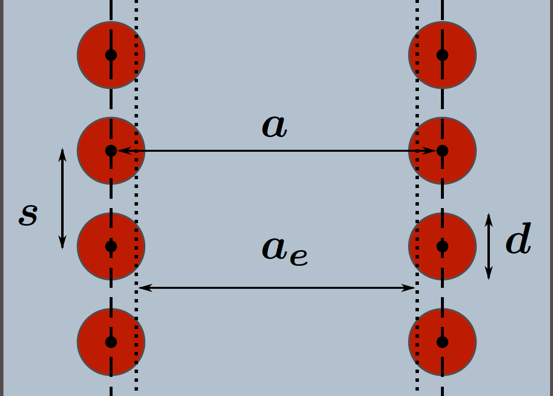
A SIW is composed of a thin dielectric substrate covered on both faces by a metallic layer. The substrate embeds two parallel rows of metallic via-holes delimiting the wave propagation area. The organization of the vias and the geometric parameters are described in the attached figure.
The width of a SIW is the distance [math]\displaystyle{ a }[/math] between its two vias rows, which is defined from center-to-center. An effective width [math]\displaystyle{ a_e }[/math] may be used to characterize more precisely the wave propagation. The distance between two successive vias of the same row is [math]\displaystyle{ s }[/math], and the vias diameter is denoted by [math]\displaystyle{ d }[/math].
1.2. Transverse Magnetic Propagation Modes
In classical solid-walled rectangular waveguide, the general formulation of propagation involves a superposition of transverse electric (TE) and transverse magnetic (TM) modes. Each of these is associated with particular fields and currents. In the case of TM modes, the current in the vertical walls is longitudinal, i.e. parallel to the propagation axis, usually denoted as [math]\displaystyle{ z }[/math]. Then, given the vertical geometry of the vias, it is impossible for such modes to appear in SIW's: the electrical current cannot propagate from via to via. Only TE modes are able to propagate through SIW.
Each mode appears above a precise cut-off frequency determined by the waveguide dimensions and the filling medium. For TM modes, decreasing the waveguide thickness (usually denoted as [math]\displaystyle{ b }[/math]) increases the cut-off frequency with [math]\displaystyle{ 1/b }[/math]. In the case of SIW, the thickness is so low that the cut-off frequency of TM modes is much higher than the dominant mode.
1.3. Effective Width
One of the objectives of the SIW geometry is to reproduce the characteristic propagation modes of rectangular waveguides inside a thin template. The width [math]\displaystyle{ a }[/math] of the waveguide is an essential parameter of those modes. In the typical SIW geometry, [math]\displaystyle{ a }[/math] is the distance between the two vias rows from center-to-center (see figure). Due to the vias geometry, this distance cannot be utilized directly; because of the space between successive vias and their circular shape, the signal inside the guide does not behave exactly as it would in a perfectly rectangular waveguide of the same width.
To apply waveguide theory to SIWs, an effective width [math]\displaystyle{ a_\text{eff} }[/math]can be used. Its takes into account the shape of the vias and the space in-between. Its value lies between [math]\displaystyle{ a + d }[/math] and [math]\displaystyle{ a - d }[/math].
A common simple definition is[1][2]
[math]\displaystyle{ a_\text{eff} = a - \frac{d^2}{0.95 s} }[/math]
and a more refined definition used for large values of [math]\displaystyle{ d/a }[/math] is[3]
[math]\displaystyle{ a_\text{eff} = a - 1.08 \frac{d^2}{s} + 0.1 \frac{d^2}{a}. }[/math]
Using this effective width, the propagation constant of a SIW will be similar to that of a classical rectangular waveguide whose width is [math]\displaystyle{ a_\text{eff} }[/math]. The formulas given above are empirical: they were established comparing the dispersion characteristics of different SIWs to those of rectangular waveguide filled with the same dielectric material.[2]
2. Transitions
SIWs are promising structures that can be used in complex microwave systems as interconnects, filters, etc. However, a problem may arise: the connection of the SIWs with other kinds of transmission lines (TL), mainly microstrip, coplanar and coaxial cable. The goal of such transitions between two different topologies of TL is to excite the correct transmission mode in the SIW cavity with the minimum loss of power and on the broadest possible frequency range.
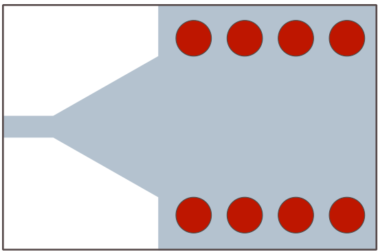
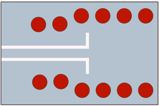
Rapidly after the presentation of the concept of SIW by Ke Wu, two different transitions were mainly used.[4][5] First, the tapered transition allowing to convert a microstrip line into a SIW and secondly a transition between a coplanar line and a SIW (see attached figure). The tapered transition from microstrip to SIW is useful for thin substrates. In this case, the radiation losses associated with microstrip lines are not too significant. This transition is massively used and different optimizing process have been proposed.[6][7] But this is not applicable to thick substrates where leakages are important. In that situation, a coplanar excitation of the SIW is recommended. The drawback of the coplanar transition is the narrower bandwidth.
These two kinds of transitions involve lines that are embedded in the same substrate, which is not the case for coaxial lines. There exists no direct transition between a coaxial line and a SIW: an other planar line have to be used to convert properly the coaxial TEM propagation modes to the TE modes in SIW.
Several studies have been carried out to optimize the transition between topologies without being able to determine a universal rule making it possible to draw the absolute transition. The architecture, the frequency range, the used materials, etc. are examples of parameters that make specific the design procedure.[1][8][9][10]
3. Losses in SIW
The propagation constant of a transmission line is often decomposed as follow :
[math]\displaystyle{ \gamma = \alpha + j \beta }[/math]
and the oscillating electric and magnetic fields in the guide have the form[11][math]\displaystyle{ \begin{align} H_{x,y,z}(x,y,z) &= h_{x,y,z} e^{- \gamma z} = h_{x,y,z} e^{- \alpha z} e^{- j \beta z} \\ E_{x,y,z}(x,y,z) &= e_{x,y,z} e^{- \gamma z} = e_{x,y,z} e^{- \alpha z} e^{- j \beta z} \end{align} }[/math]It is then clear that, while the imaginary part of [math]\displaystyle{ \gamma }[/math] stands for the propagating component, the real component [math]\displaystyle{ \alpha }[/math] describes the loss of intensity during the propagation. This loss is generated by different phenomena and each of them is represented by a term [math]\displaystyle{ \alpha }[/math]. The most common terms are the following:[11][12]
- [math]\displaystyle{ \alpha_C }[/math] : the loss due to the external metal conductivity
- [math]\displaystyle{ \alpha_D }[/math] : the loss due to loss tangent of the dielectric medium filling the waveguide
- [math]\displaystyle{ \alpha_G }[/math] : the loss due to conductivity of the dielectric medium filling the waveguide
- [math]\displaystyle{ \alpha_R }[/math] : the loss due to radiation.
This decomposition is valid for all kind of transmission lines. However, for rectangular waveguides, the attenuation due to radiations and substrate conductivity is negligible. Indeed, usually, the substrate is an insulator such that [math]\displaystyle{ \alpha_G \simeq 0 }[/math]. In the same way, if the wall thickness is much thicker than the skin depth of the signal, no radiation will appear. This is in fact one of the advantages of closed waveguides compared to open lines such as microstrips.
The SIWs show comparable or lower losses compared the other traditional planar structures like microstrip or coplanar lines especially at high frequencies.[1] If the substrate is thick enough, the losses are dominated by the dielectric behavior of the substrate.[13]
3.1. Attenuation due to Conduction Currents
Part of the signal attenuation is due to the surface current density flowing through the metallic walls of the waveguide. These currents are induced by the propagating electromagnetic fields. These losses may also be named ohmic losses for obvious reasons. They are linked to the finite conductivity of the metals: the better the conduction, the lower the losses. The power lost per unit length [math]\displaystyle{ P_l }[/math] can be calculated by integrating the current densities [math]\displaystyle{ J_s }[/math] on a path [math]\displaystyle{ C }[/math] enclosing the waveguide walls :[11]
[math]\displaystyle{ P_l = \frac{1}{2} R_s \int_C |{J_s}|^2 dl. }[/math]
It can be shown that in a classical rectangular waveguide, the attenuation of the dominant mode [math]\displaystyle{ \text{TE}_{10} }[/math] due to conduction currents is given, in Nepers per meter, by[math]\displaystyle{ \alpha_C = \frac{R_s}{a^3 b \beta k \eta} \left( 2 b \pi^2 + a^3 k^2 \right) = \frac{R_s}{\beta k \eta} \left( \frac{2 \pi^2}{a^3 } + \frac{k^2}{b} \right) }[/math]where
- [math]\displaystyle{ a }[/math] is the width of the waveguide
- [math]\displaystyle{ b }[/math] its height
- [math]\displaystyle{ \eta = \sqrt{\mu / \epsilon} }[/math] the wave impedance
- [math]\displaystyle{ k = \omega \sqrt{\mu \epsilon} }[/math] the wave vector
- [math]\displaystyle{ \delta = 1 / \sqrt{\pi f \mu \sigma} }[/math] the skin depth in the conductor
- [math]\displaystyle{ R_s = \frac{1}{\delta \sigma} = \sqrt{\frac{\omega \mu}{2 \sigma}} }[/math] is the sheet resistance (of surface impedance).
It is noticeable that [math]\displaystyle{ \alpha_C }[/math] is directly linked to the substrate thickness [math]\displaystyle{ b }[/math]: the thinner the substrate, the higher the conduction losses. This can be explained keeping in mind that this ohmic losses are determined by integrating the current density on a path enclosing the waveguide walls.
On the top and bottom horizontal metallic plates, the current is scaled with [math]\displaystyle{ 1/b }[/math], due to the modification of the field intensity on these plates: when [math]\displaystyle{ b }[/math] increases, the field intensity decreases as well as the currents. In the vertical walls, this variation of [math]\displaystyle{ J_s^2 }[/math] is compensated by the lengthening of the integration path [math]\displaystyle{ C }[/math]. As a result, the contribution of the vertical vias to the conductor losses is unchanged with [math]\displaystyle{ b }[/math].[14] That is the reason why there is two terms in the expression of [math]\displaystyle{ \alpha_C }[/math]: the first is independent of [math]\displaystyle{ b }[/math] while the second one varies with [math]\displaystyle{ 1/b }[/math].
Another key point of the conduction losses experienced by the SIWs is linked to the roughness of the surfaces that may appear due to the synthesis processes. This roughness decreases the effective conductivity of the metallic walls and subsequently increases the losses. This observation is of crucial importance for the design of SIWs as they are integrated on very thin substrates. In this case, the contribution of the conduction losses on the global attenuation is predominant.[1][13][15]
3.2. Attenuation due to Dielectric Substrate
The attenuation due to the dielectric behavior of the filling medium can be determined directly from the propagation constant.[11] Indeed, it can be proven that, making use of a Taylor expansion of the function [math]\displaystyle{ \sqrt{a^2 + x^2} }[/math] for [math]\displaystyle{ x \ll a }[/math], the propagation constant is[math]\displaystyle{ \gamma = \alpha_D + j \beta \simeq \frac{k^2 \tan{\delta}}{2 \beta} + j\beta }[/math]where [math]\displaystyle{ \tan \delta }[/math] is the loss tangent of the dielectric substrate. This approximation is correct if [math]\displaystyle{ \tan{\delta} \ll 1 }[/math] which is usually the case in microwave electronics (at 10 GHz, [math]\displaystyle{ \tan{\delta} = 0 }[/math] in air, [math]\displaystyle{ 1.5 \times 10^{-4} }[/math] in Teflon and [math]\displaystyle{ 1 \times 10^{-4} }[/math] in bulk alumina). Then, the following identification can be made:[math]\displaystyle{ \alpha_D = \frac{k^2 \tan{\delta}}{2 \beta}. }[/math]This relation is correct for both electrical and magnetic transverse modes.
The dielectric losses [math]\displaystyle{ \alpha_D }[/math] depend only on the substrate and not on the geometry: unlike the conduction losses, [math]\displaystyle{ \alpha_D }[/math] is not influenced by the substrate thickness. It transpires that the only way to reduce [math]\displaystyle{ \alpha_D }[/math] consists in choosing a template with better dielectric properties: the lower the loss tangent [math]\displaystyle{ \tan{\delta} }[/math], the lower the attenuation.
3.3. Attenuation due to Radiation
Because the vertical walls of the SIW are not continuous, radiation leakages may flow between the vias. These leakages can significantly affect the global transmission quality if the vias geometry is not chosen carefully. Some studies have been conducted to describe, predict and reduce the radiation losses. They have resulted in some simple geometric rules that have to be satisfied in order to reduce the radiation losses.[3][4][14][16][17]
The geometric parameters of interest are the diameter [math]\displaystyle{ d }[/math], the spacing [math]\displaystyle{ s }[/math] and the center-to-center distance between the vias [math]\displaystyle{ a }[/math]. They must be tuned in such a way to approximate the behavior of a continuous metallic wall: the spacing of the vias has to remain small compared to their diameter, while the diameter must be small compared to the waveguide width (or waveguide wavelength). To keep the radiation losses reasonably small, the recommended values are[math]\displaystyle{ s \leq 2 d ~~~~~~ \textrm{and} ~~~~~~ d \leq \frac{a}{5}. }[/math]For a specific traveling mode, the leakages decrease with the increasing frequency and are maximal at the cut-off frequency of the mode. The radiation leakage factor [math]\displaystyle{ \alpha_R }[/math] is independent of the substrate properties and independent of the height of the guide.
The content is sourced from: https://handwiki.org/wiki/Engineering:Substrate_integrated_waveguide
References
- Bozzi, M.; Georgiadis, A.; Wu, K. (2011). "Review of substrate-integrated waveguide circuits and antennas" (in en). IET Microwaves, Antennas & Propagation 5 (8): 909. doi:10.1049/iet-map.2010.0463. https://digital-library.theiet.org/content/journals/10.1049/iet-map.2010.0463.
- Cassivi, Y.; Perregrini, L.; Arcioni, P.; Bressan, M.; Wu, K.; Conciauro, G. (September 2002). "Dispersion characteristics of substrate integrated rectangular waveguide". IEEE Microwave and Wireless Components Letters 12 (9): 333–335. doi:10.1109/LMWC.2002.803188. ISSN 1531-1309. https://ieeexplore.ieee.org/document/1031925.
- Feng Xu; Ke Wu (January 2005). "Guided-wave and leakage characteristics of substrate integrated waveguide". IEEE Transactions on Microwave Theory and Techniques 53 (1): 66–73. doi:10.1109/TMTT.2004.839303. ISSN 0018-9480. Bibcode: 2005ITMTT..53...66X. https://ieeexplore.ieee.org/document/1381676.
- Ke Wu; Desiandes, D.; Cassivi, Y. (2003). "The substrate integrated circuits - a new concept for high-frequency electronics and optoelectronics". 6th International Conference on Telecommunications in Modern Satellite, Cable and Broadcasting Service, 2003. TELSIKS 2003. (Serbia, Montenegro, Nis: IEEE) 1: P–III–P-X. doi:10.1109/TELSKS.2003.1246173. ISBN 978-0-7803-7963-3. https://ieeexplore.ieee.org/document/1246173.
- Deslandes, D.; Ke Wu (2001). "Integrated transition of coplanar to rectangular waveguides". 2001 IEEE MTT-S International Microwave Sympsoium Digest (Cat. No.01CH37157) (Phoenix, AZ, USA: IEEE) 2: 619–622. doi:10.1109/MWSYM.2001.966971. ISBN 978-0-7803-6538-4. https://ieeexplore.ieee.org/document/966971.
- Rayas-Sanchez, Jose E.; Gutierrez-Ayala, Vladimir (2008). "A general EM-based design procedure for single-layer substrate integrated waveguide interconnects with microstrip transitions". 2008 IEEE MTT-S International Microwave Symposium Digest: 983–986. doi:10.1109/MWSYM.2008.4632999. ISBN 978-1-4244-1780-3. https://ieeexplore.ieee.org/document/4632999.
- Deslandes, Dominic (2010). "Design equations for tapered microstrip-to-Substrate Integrated Waveguide transitions". 2010 IEEE MTT-S International Microwave Symposium: 704–707. doi:10.1109/MWSYM.2010.5517884. ISBN 978-1-4244-6056-4. https://ieeexplore.ieee.org/document/5517884.
- Chen, Xiao-Ping; Wu, Ke (2009). "Low-loss ultra-wideband transition between conductor-backed coplanar waveguide and substrate integrated waveguide". 2009 IEEE MTT-S International Microwave Symposium Digest: 349–352. doi:10.1109/MWSYM.2009.5165705. ISBN 978-1-4244-2803-8. https://ieeexplore.ieee.org/document/5165705.
- Lee, Sunho; Jung, Sangwoon; Lee, Hai-Young (2008). "Ultra-Wideband CPW-to-Substrate Integrated Waveguide Transition Using an Elevated-CPW Section". IEEE Microwave and Wireless Components Letters 18 (11): 746–748. doi:10.1109/LMWC.2008.2005230. ISSN 1531-1309. https://ieeexplore.ieee.org/document/4666756.
- Taringou, Farzaneh; Bornemann, Jens (2011). "New substrate-integrated to coplanar waveguide transition". 2011 41st European Microwave Conference: 428–431. doi:10.23919/EuMC.2011.6101767. https://ieeexplore.ieee.org/document/6101767.
- Pozar, David M. (2012). Microwave engineering. ISBN 978-81-265-4190-4. OCLC 884711361. http://worldcat.org/oclc/884711361.
- "Microwaves101 | Waveguide Loss". https://www.microwaves101.com/encyclopedias/waveguide-loss.
- Van Kerckhoven, Vivien (2019). Nanowire-based microwave devices in substrate integrated waveguide topology using a laser-assisted fabrication process (Thesis). UCL - Université Catholique de Louvain. https://dial.uclouvain.be/pr/boreal/object/boreal:222909
- Bozzi, M.; Perregrini, L.; Ke Wu (2008). "Modeling of Conductor, Dielectric, and Radiation Losses in Substrate Integrated Waveguide by the Boundary Integral-Resonant Mode Expansion Method". IEEE Transactions on Microwave Theory and Techniques 56 (12): 3153–3161. doi:10.1109/TMTT.2008.2007140. ISSN 0018-9480. Bibcode: 2008ITMTT..56.3153B. https://ieeexplore.ieee.org/document/4682637.
- Lomakin, Konstantin; Gold, Gerald; Helmreich, Klaus (2018). "Analytical Waveguide Model Precisely Predicting Loss and Delay Including Surface Roughness". IEEE Transactions on Microwave Theory and Techniques 66 (6): 2649–2662. doi:10.1109/TMTT.2018.2827383. ISSN 0018-9480. Bibcode: 2018ITMTT..66.2649L. https://ieeexplore.ieee.org/document/8356729.
- Bozzi, Maurizio; Pasian, Marco; Perregrini, Luca; Wu, Ke (October 2009). "On the losses in substrate-integrated waveguides and cavities" (in en). International Journal of Microwave and Wireless Technologies 1 (5): 395–401. doi:10.1017/S1759078709990493. ISSN 1759-0787. https://www.cambridge.org/core/product/identifier/S1759078709990493/type/journal_article.
- Che, Wenquan; Wang, Dapeng; Deng, Kuan; Chow, Y. L. (October 2007). "Leakage and ohmic losses investigation in substrate-integrated waveguide: SUBSTRATE-INTEGRATED WAVEGUIDE" (in en). Radio Science 42 (5): n/a. doi:10.1029/2007RS003621. http://doi.wiley.com/10.1029/2007RS003621.