Angle-resolved photoemission spectroscopy (ARPES) is a vital technique in which spectra are collected from both the energy and momentum of photoemitted electrons and is indispensable for investigating the electronic band structure of solids.
- angle-resolved photoemission spectroscopy (ARPES)
- organic single crystals
- inorganic materials
1. Introduction
Electronic band structure is essential to explain many physical properties of solids and serves as the foundation for understanding all solid-state devices. The formation of electronic bands is mainly from the overlapping of the wavefunctions of the outermost electrons (valence electrons) of the atoms and molecules. The total width of the occupied portion of the bands below the Fermi level is typically in the order of 10 eV. The more tightly bound inner shell electrons have very narrow bands, because they do not overlap to a large extent. The electronic band structure is itself a property of the crystal, and as a result possesses the symmetry of the crystal [1].
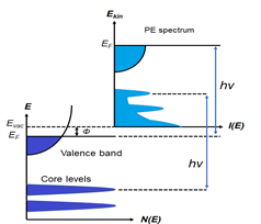
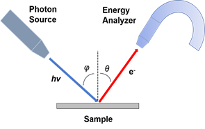
One of the most suitable and widely used techniques to study the electronic structure of a material is photoemission spectroscopy (PES) [2]. Based on the photoelectric effect as explained by Einstein in 1905 [3], photoelectrons are created via the interaction between the irradiating photons and the sample. Shown in Figure 1a is the schematic of PES. The electrons are excited by the incident photons on the sample, and if the excited electrons have sufficient energy to escape to the vacuum, they can then be detected by an electron energy analyzer. By measuring the kinetic energy and angular distribution of the electrons photoemitted from a sample illuminated with sufficiently high-energy radiation, one can gain information on both the energy and momentum of the electrons propagating inside a material. This is critical in illustrating the connection between electronic, magnetic, and chemical structure of solids.
With the unique capability to directly image and discriminate surface and bulk electronic states, ARPES has been widely used in the studies of the electronic structure of metals, semiconductors, insulators, superconductors and many other materials. The rapid progress of this technique in the recent years has developed many derivatives of ARPES, including soft-X-ray ARPES, time-resolved ARPES, spin-resolved ARPES and spatially resolved ARPES. All these techniques have been providing important insights in the research of materials.[4]
(a) (b) (c)
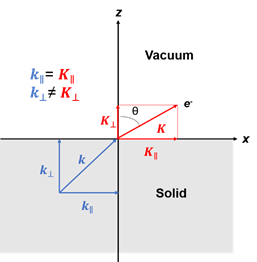
Figure 1. (a) Schematic of a photoemission experiment. The electrons are excited by the incident photons on the sample, then the excited electrons escape to the vacuum and are detected by an electron energy analyzer. (b) Schematic representation of photoemission spectroscopy (PES). The photoelectrons are excited from the occupied energy levels, including the valence bands as well as the core-level states. Additionally, secondary electrons excited by the photoelectrons that define the vacuum level cutoff are shown. (c) Photoemission geometry and relation of the electron wave vectors in vacuum (\( K \)) and in solid (\( k \)). Note that only the parallel momentum component is conserved.
2. Principle
In a simple model which does not show any energy loss during the photoemission process, the total energy must be conserved. It suggests that the kinetic energy of the emitted electrons equals the incident photon energy minus the initial binding energy (BE) of the corresponding bound electronic states. The relation can be expressed as follows [5]:

where 


Photons with a known energy are applied to excite electrons out of the sample surface in a PES experiment. The kinetic energy and the momentum of the excited electrons can be measured by an electrostatic analyzer placed close to the surface. As indicated in Figure 1b, in the schematic representation of PES, the photoelectrons are from the occupied energy levels, including the valence bands (VB) and the core-level states which correspond to the closed atomic shells. Moreover, shown schematically in Figure 1b are secondary electrons excited by the photoelectrons that define the vacuum level cutoff [6].
Another significant aspect of PES is its surface sensitivity. For this surface analytic tool, the photoexcited electrons are used as the probing particles which have a strong interaction with the solid, leading to a relatively short escape distance, known as the mean free path (MFP. The MFP is the average distance that the particles can travel between inelastic collisions. It strongly depends on the kinetic energy of the photoelectron and is relatively independent of the materials [7]. The thickness of a monolayer is material dependent, typically ranging from 0.2–0.4 nm. It is noticed that, within the energy range of interest, which is between 10 to 2000 eV, the MFP is in the order of only 1–10 monolayers, depending on the kinetic energy of the photoelectrons.
In a photoemission process, not only the energy but also the momentum can be observed. The energy band dispersion E(\( k \)) of a crystalline sample can be obtained if the momentum of the photoelectrons is also measured in addition to the kinetic energy with an angle-resolved electron energy analyzer. This technique is named as angle-resolved photoemission spectroscopy (ARPES) [8][9].
Figure 1c is the photoemission geometry and the relation of the electron wave vectors in vacuum (\( K \)) and in solid (\( k \)). The final states in the solid can be assumed as the free-electron-like dispersion, and the energy of the excited electrons before escaping the surface is:

where 


where 


Note in Figure 1c that the parallel momentum component is conserved (


where \( m \) can be taken as \( m_o \) if the final state is of high enough energy. The band dispersions along with the 


3. Applications
3.1 Organic Charge Transfer Conductors
One of the organic charge transfer crystals first studied with ARPES is a bis(ethylenedithio)-tetrathiafulvalene (BEDT-TTF) derivative, a-(BEDT-TTF)2I3 [10]. It undergoes a metal-to-insulator transition at 135 K [11], but the b phase has a superconducting ground state, Tc = 1.5 K [12]. These facts make (BEDT-TTF)2I3 suitable for studies of the relationship between the crystal structure and electronic properties. The crystal is triclinic with the unit cell described by a = 9.211 Å, b = 10.850 Å, c = 17.488 Å, a = 96.95°, b = 97.97°, and g = 90.75° [13]. The ARPES investigation was on in situ cleaved single crystals [10].
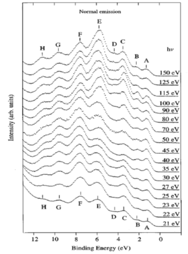
Shown in Figure 2 are ARPES spectra of the valence-band regime of an a-(BEDT-TTF)2I3 crystal recorded in normal emission, with different photon energies in the range 21–150 eV [10]. The spectra in this figure are normalized to the same height for visual clarity. Eight peaks labeled A–H can be seen in the valence-band regime shown in Figure 2, having binding energies between 1.2 and 10.9 eV relative to the Fermi level. The binding energies (BE) for peaks A–H are 1.2, 2.1, 3.4, 4.1, 5.7–6.0, 7.6, 9.6, and 10.9 eV, respectively. All peaks exist in the spectra except the peak D, which reduces to a shoulder when the excitation photon energy is greater than 70 eV or less than 25 eV. Within the experimental resolution, all peak BEs are independent of the exciting photon energy except that of peak E, whose dependence on the photon energy does not seem to be random. When the photon energy decreases from 150 ev to 50 ev, the peak shape changes gradually. Combined with the shift of the peak position when the photon energy is decreased below 70 eV, it is reasonable to expect that the peak consists of two closely lying structures. The change of the peak shape and the BE can be interpreted as the structure with the lowest binding energy dominating at photon energies above 70 eV, and the other structure is seen as a shoulder on the high BE side of the dominating structure. The structure with higher BE is dominating at lower photon energies, while the other is not identified when photon energies are below 30 eV. The ARPES data presented in Figure 2 gave no support for dispersing bands in the G-Z (kz) direction. Angle-resolved measurements along the a and b axis also gave no evidence that the structures closest to the Fermi level have any dispersion in the highly conducting plane. An upper limit of about 0.25 eV for the dispersion is set by the experiment [10]. The most probable explanations for the lack of any dispersion and the lack of a sharp Fermi edge despite a-(BEDT-TTF)2I3 showing metallic transport properties are correlation effects or the calculated narrow-gap semiconductor band structure [10].
Figure 2. Angle-resolved photoemission spectroscopy (ARPES) photoemission spectra of a-(BEDT-TTF)2I3 obtained in normal emission, with photon energies between 21 and 150 eV. Different structures in the valence band regime are labeled A to H and marked with tick marks in the spectra. The spectra are normalized to the same height. From Ref. [10] with permission.
3.2 Organic Semiconductors
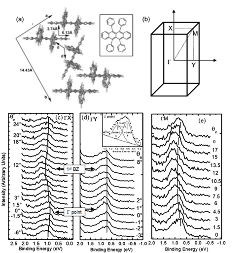
The interest in organic electronics was boosted with the discovery of conducting polymers in the early 1980s, which earned Alan Heeger, Alan MacDiarmid, and Hideki Shirakawa the Nobel Prize in Chemistry in 2000 [14], and was further stimulated when organic light-emitting diodes with quantum efficiencies attractive for consideration in real applications [15][14]. Rubrene is a tetraphenyl derivative of tetracene and has been shown by Podzorov et al. to have a field-induced hole mobility of over 15 cm2V−1s−1 at room temperature, with a novel device structure [16][17]. The molecular and crystal structure of rubrene are presented in Figure 3 [18]. Rubrene crystals are of the orthorhombic pyramidal point group with a well-developed face in (001) direction (a-b plane) and the slow-growing axis (c-axis) is normal to the top surface. Inside the crystal the rubrene molecules are in a lying down phase with long axes all embedded in the a-b plane. Figure 3b shows the reciprocal lattice of the rubrene single crystal unit cell, where the ΓX, ΓY and ΓM direction corresponds to the a-axis, b-axis and the diagonal direction, respectively. Figure 3c–e respectively show the ARPES spectra of rubrene single crystal surface measured along the X (a-axis), the Y (b-axis) and the M (diagonal) directions, respectively, as a function of electron emission angle.
Figure 3. (a) Illustration of the lattice parameters within the a-b plane of rubrene single crystal. The molecular structure of rubrene is also shown in the inset. (b) The reciprocal lattice of crystalline rubrene. ΓX, ΓY and ΓM correspond to the a, b and the diagonal crystalline direction, respectively. Evolution of the highest occupied molecular orbital (HOMO) region in the rubrene ARPES spectra as a function of electron emission angle (θ) for single crystal rubrene along (c) ΓX, (d) ΓY, and (e) ΓM direction. From Ref. [18] with permission.
3.3 Organo-Metallic Perovskite Charge Transfer Crystals
Perovskite is the appellation for any materials that have the same crystal structure as calcium titanate, namely, ABX3. Perovskites are originated from a cubic structure, where A is commonly a large cation at the body center of a cubic unit cell, B a smaller metal atom at the 8 corners of the cube, each contributing 1/8 of an atom to the unit cell, and X anions are at the middle of the 12 edges of the cube, each contributing 1/4 of an atom to the unit cell [19][20][21]. Some perovskites are reported as non-cubic. For example, CsPbI3 has an orthorhombic structure at room temperature [22]. The crystal structure of BiFeO3 multiferroic thin film is monoclinic in contrast to bulk, which is rhombohedral [23]. Organo-metallic halide perovskites, with organic A cations such as methylammonium (MA=CH3NH3+) or formamidinium (FA=CH(NH2)2+), B of group 14 metal Pb or Sn, and X of halogen elements Cl, Br, and I.X3, which are tetragonal, have exhibited important and unique properties. In just about a decade, maximum power conversion efficiencies (PCEs) have evolved from 3.8% [24] in 2009 to 23.34% [25] in 2018. Monolithic tandem c-Si/perovskite solar cells have achieved high efficiencies above 27% [26], with a potential of above 30%[27]. Other applications of organo-metallic halide perovskites beyond just photovoltaic devices include photo detectors [28], light emitting diodes (LED) [29] and lasers [30].
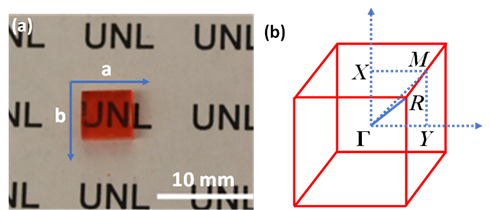
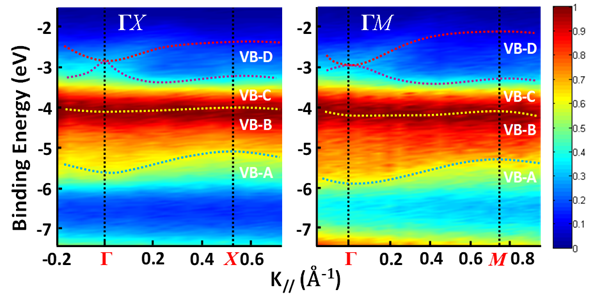
Figure 4a shows an as-grown methylammonium lead bromide (MAPbBr3) single crystal. The reciprocal lattice of the crystal unit cell, where ΓX, ΓY, and ΓM directions correspond to the a-axis, b-axis (Figure 4a) and the face diagonal direction, respectively. The reciprocal lattice is often used to represent the Fourier transform of the crystal lattice in k-space. Because of the restriction of the intrinsic (001) cleavage plane of the perovskite material, ΓR direction could not be evaluated. ΓX, ΓY and ΓZ directions are all degenerate due to crystal symmetry [31]. Figure 5 shows the MAPbBr3 energy dispersions of the four valence bands as a function of 

Figure 4. (a) MAPbBr3 single crystal with a surface area of 6 mm × 6 mm. (b) The reciprocal lattice of the cubic MAPbBr3. From Ref. [31] with permission.
Figure 5. Energy distribution curves (EDCs) of MAPbBr3 along ΓX and ΓM directions. The color represents the intensity of the photoemission spectrum. From Ref. [31] with permission.
3.4 Three-Dimensional Topological Insulators
Three dimensional topological insulators are nonmagnetic insula-tors which possess metallic surface states (SSs) as a consequence of the nontrivial topology of electronic wavefunctions in the bulk of the material. The first 3D topological insulator that was discovered experimentally is the Bi1-xSbx semiconducting alloy, which unusual surface bands were mapped with ARPES. The 3D topological state in Bi1-xSbx is a new state that cannot be reduced to a quantum spin Hall state [32][33][34]. Electrons' spin and linear momentum are locked one to one on the surface, which is a new form of 2D metal. And the two dimensional Fermi surface carries a nontrivial Berry phase of π [33]. The following way can be used to understand its uniqueness: A layered three-dimensional version of the quantum spin Hall insulator Hg(Cd)Te would be a weak (3D) topological insulator (WTI) with an invariant structure of (Vo = 0,111). A WTI would show that SSs contain an even number of Dirac cones and thus a net Berry’s phase of 0 or 2π.
ARPES measure the distribution of spin orientations on the Fermi surface when carried out in a spin resolution mode. It can be used to estimate the Berry’s phase on the surface. Spin sensitivity is critically important for probing the existence of spin-momentum locking on the surface, which is expected as a consequence of bulk topological order. However, the 3D topological insulator Bi1-xSbx has an odd number of SSs whose spin texture supports a nontrivial Berry’s phase providing protection against nonmagnetic disorder. This kind of topological insulator is described by (Vo = 1,).
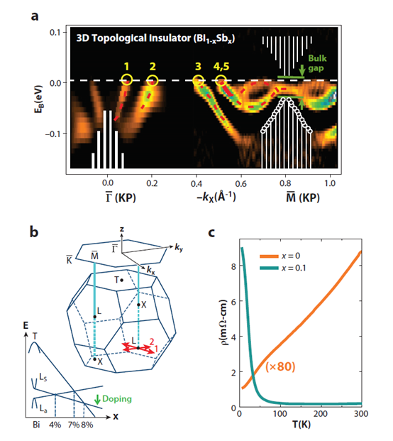
It can be observed that a narrow electron pocket that is doubly degenerate around in the Bi-Sb alloy (Figure 6). This is indicated by its splitting below EF between -kx = 0.55A-1 and , as well as the fact that this splitting goes to zero at according to Kramers’ theorem. Unlike in Bi, the states near fall completely inside the bulk energy gap in Bi0.9Sb0.1, which preserves their purely surface character at . The surface Kramers point is located about 15 ± 5 meV below EF at = . The observation of five SS crossings (an odd rather than an even number) between and , confirmed by the observation of the Kramers degenerate point confirms the topologically nontrivial nature of the material. Although these results are consistent with a Z2 topological insulator scenario for Bi-Sb, more decisive evidence comes from the study of the spin texture of the surface Fermi surface.[35]
Figure 6. Topological surface states (SSs) in Bi1-xSbx. Topological insulator Bi-Sb alloy exhibits an odd number of SS crossings between any pair of Kramers points. (a) Bi-Sb alloy in the semiconducting composition range (0.07 < x < 0.18) exhibits an odd number of SS Fermi crossings in between any pair of Kramers points. (b) A schematic of the 3D Brillioun zone (BZ) and its (111) hexagonal surface projection is shown. The green arrow indicates the doping shown in panel c. (c) Resistivity profile of pure Bi (semimetallic) is compared with a semiconducting Bi-Sb alloy. The percentage of Sb is indicated by x. From Ref [35].
3.5 Superconductors
Sr2RuO4 has low-energy electronic structure, as predicted by band structure calculations, which is characterized by three bands crossing the chemical potential[36][37]. As shown in Figure. 6(d), it defines a complex Fermi surface which contains two electron pockets and one hole pocket. They have been clearly observed in de Haas–van Alphen experiments [38][39]. Figure 7(a) and (b) show high resolution ARPES data (ΔE = 14 meV; Δk =1.5% of the zone edge) taken at 10K with 28 eV photons on a Sr2RuO4 single crystal cleaved at 180K which suppresses the reconstructed-surface contributions to the photoemission signal and allows one to isolate the bulk electronic structure [40]. Many well defined quasiparticle peaks disperse towards the Fermi energy and disappear upon crossing EF: As shown in Figure 7c, a Fermi energy intensity map can be obtained by integrating the spectra over a narrow energy window about EF(±10 meV): As the spectral function (multiplied by the Fermi function) reaches its maximum at EF when a band crosses the Fermi energy, the Fermi surface is identified by the local maxima of the intensity map. Following this method, in Figure 7d, the three sheets of Fermi surface are clearly resolved and are in excellent agreement with the theoretical calculations.[41]
Figure 7. ARPES spectra and corresponding intensity plot from Sr2RuO4 along (a) Γ-M; and (b) M-X. (c) Measured and (d) calculated [42] Fermi surface. All data were taken at 10K on a Sr2RuO4 single crystal cleaved at 180K. From Ref. [40].
This entry is adapted from the peer-reviewed paper 10.3390/cryst10090773
References
- Ashcroft, N.W. and N.D. Mermin, Solid State Physics. 1976, New York: Harcourt.
- Hüfner, S., Photoelectron Spectroscopy: Principles and Applications;. 2003, Germany: Springer.
- Einstein, A., On a Heuristic Viewpoint Concerning the Production and Transformation of Light. Annalen der Physik, 1905. 17: p. 132-148.
- Cite this articleLv, B., Qian, T. & Ding, H. Angle-resolved photoemission spectroscopy and its application to topological materials. Nat Rev Phys 1, 609–626 (2019). https://doi.org/10.1038/s42254-019-0088-5
- Park, R.L. and M.G. Lagally, Solid state physics: surfaces. Vol. 22. 1985: Academic Press.
- Reinert, F. and S. Hüfner, Photoemission spectroscopy—from early days to recent applications. New Journal of Physics, 2005. 7(1): p. 97.
- Seah, M., MP Seah and WA Dench, Surf. Interface Anal. 1, 2 (1979). Surf. Interface Anal., 1979. 1: p. 2.
- Smith, K.E. and S.D. Kevan, The electronic structure of solids studied using angle resolved photoemission spectroscopy. Progress in solid state chemistry, 1991. 21(2): p. 49-131.
- Damascelli, A., Z. Hussain, and Z.-X. Shen, Angle-resolved photoemission studies of the cuprate superconductors. Reviews of modern physics, 2003. 75(2): p. 473.
- Soderholm, S., R.T. Girard, and D. Schweitzer, Electronic structure of the organic conductor alpha-(BEDT-TTF)(2)I-3 studied by angle-resolved and core-level photoelectron spectroscopy. Physical Review B, 1997. 55(7): p. 4267-4274.
- Hennig, I., et al., α And β-(BEDT-TTF)2 +I− 3: Two Dimensional Organic Metals. Molecular Crystals and Liquid Crystals, 1985. 119(1): p. 337-341.
- Yagubskii, E.B., et al., Normal-pressure superconductivity in an organic metal (BEDT-TTF) 2I3 [bis (ethylene dithiolo) tetrathiof ulvalene triiodide]. JETP Lett. , 1984. 39(1): p. 12-16.
- Bender, K., et al., Synthesis, Structure and Physical Properties of a Two-Dimensional Organic Metal, Di[bis(ethylenedithiolo)tetrathiofulvalene] triiodide, (BEDT-TTF)+ 2 I− 3. Molecular Crystals and Liquid Crystals, 1984. 108(3-4): p. 359-371.
- Burroughes, J.H., et al., Light-emitting diodes based on conjugated polymers. Nature, 1990. 347(6293): p. 539-541.
- Heeger, A.J., et al., Solitons in conducting polymers. Reviews of Modern Physics, 1988. 60(3): p. 781-850.
- Sundar, V.C., et al., Elastomeric transistor stamps: Reversible probing of charge transport in organic crystals. Science, 2004. 303(5664): p. 1644-1646.
- Podzorov, V., et al., Intrinsic charge transport on the surface of organic semiconductors. Physical Review Letters, 2004. 93(8): p. 086602.
- Ding, H.J., et al., Band structure measurement of organic single crystal with angle-resolved photoemission. Applied Physics Letters, 2010. 96(22): p. 222106.
- Hodes, G., Perovskite-Based Solar Cells. Science, 2013. 342(6156): p. 317-318.
- Lin, Q.Q., et al., Organohalide Perovskites for Solar Energy Conversion. Accounts of Chemical Research, 2016. 49(3): p. 545-553.
- Snaith, H.J., Perovskites: The Emergence of a New Era for Low-Cost, High-Efficiency Solar Cells. Journal of Physical Chemistry Letters, 2013. 4(21): p. 3623-3630.
- Li, Z., et al., Stabilizing Perovskite Structures by Tuning Tolerance Factor: Formation of Formamidinium and Cesium Lead Iodide Solid-State Alloys. Chemistry of Materials, 2016. 28(1): p. 284-292.
- Wang, J., et al., Epitaxial BiFeO3 multiferroic thin film heterostructures. Science, 2003. 299(5613): p. 1719-1722.
- Kojima, A., et al., Organometal Halide Perovskites as Visible-Light Sensitizers for Photovoltaic Cells. Journal of the American Chemical Society, 2009. 131(17): p. 6050-6051.
- Jeon, N.J., et al., A fluorene-terminated hole-transporting material for highly efficient and stable perovskite solar cells. Nature Energy, 2018. 3(8): p. 682-689.
- Werner, J., et al., Efficient Monolithic Perovskite/Silicon Tandem Solar Cell with Cell Area > 1 cm(2). Journal of Physical Chemistry Letters, 2016. 7(1): p. 161-166.
- Albrecht, S., et al., Monolithic perovskite/silicon-heterojunction tandem solar cells processed at low temperature. Energy & Environmental Science, 2016. 9(1): p. 81-88.
- Wei, H., et al., Sensitive X-ray detectors made of methylammonium lead tribromide perovskite single crystals. Nature Photonics, 2016. 10(5): p. 333-339.
- Tan, Z.-K., et al., Bright light-emitting diodes based on organometal halide perovskite. Nature nanotechnology, 2014. 9(9): p. 687-692.
- Deschler, F., et al., High photoluminescence efficiency and optically pumped lasing in solution-processed mixed halide perovskite semiconductors. The journal of physical chemistry letters, 2014. 5(8): p. 1421-1426.
- Wang, C.C., et al., Valence band dispersion measurements of perovskite single crystals using angle-resolved photoemission spectroscopy. Physical Chemistry Chemical Physics, 2017. 19(7): p. 5361-5365.
- Moore JE, Balents L. 2007. Phys. Rev. B 75:121306(R)
- Fu L, Kane CL, Mele EJ. 2007. Phys. Rev. Lett. 98:106803
- Roy R. 2009. Phys. Rev. B 79:195322
- M. Zahid Hasan, Joel E. MooreAnnual Review of Condensed Matter Physics 2011 2:1, 55-78
- Singh, D. J., Phys. Rev. B 52, 1358 (1995).
- Oguchi, T., Phys. Rev. B 51, 1385 (1995).
- Mackenzie, A. P. et al., Phys. Rev. Lett. 76, 3786 (1996).
- Bergemann, C., Julian, S. R., Mackenzie, A. P., NishiZaki, S. andMaeno, Y., Phys. Rev. Lett. 84, 2662 (2000).
- Damascelli, A. et al., Phys. Rev. Lett. 85, 5194 (2000).
- Damascelli, Andrea. "Probing the electronic structure of complex systems by ARPES." Physica Scripta 2004.T109 (2004): 61.
- Mazin, I. I. and Singh, D. J., Phys. Rev. Lett. 79, 733 (1997).

