Your browser does not fully support modern features. Please upgrade for a smoother experience.
Please note this is an old version of this entry, which may differ significantly from the current revision.
Sn-rich solder joints in three-dimensional integrated circuits and their reliability issues, such as electromigration (EM), thermomigration (TM), and thermomechanical fatigue (TMF), have drawn attention related to their use in electronic packaging. The Sn grain orientation is recognized as playing an important role in reliability issues due to its anisotropic diffusivity, mechanical properties, and coefficient of thermal expansion.
- lead-free solder
- Sn grain orientation
- electromigration
1. Introduction
Lead-free solder has been widely used in electronic packaging since the restriction of the inclusion of lead in consumer electronics [1][2][3]. Lead-free solders are Sn-based alloys with various kinds of element additions, including Ag, Cu, Ni, Bi, Zn, Ti, In, and graphene [4][5][6][7][8][9][10]. Such alloys possess a wide range of melting points, electrical and mechanical properties, microstructures, and wetting behaviors for various applications in electronic devices [11][12][13][14][15]. Among them, Sn-rich solder, which contains considerable amounts of Sn in the solder matrixes, is widely adopted in solder joints that are assembled via under-bump metallization (UBM), using a solder alloy and intermetallic compound (IMC) at the interface between the solder and the UBM method via a reflow process at a suitable temperature [16][17][18]. The reliability issues of Sn-rich solder joints have drawn substantial concerns, the first of which is the electromigration (EM) reliability during a consistent electron flow with a critical current density in Sn-rich solder joints [19][20][21], inducing UBM dissolution, rapid IMC growth, void formation, and severe Joule heating [22][23][24][25]. Then, the Joule heating induces a temperature gradient in the solder joint, known as the thermomigration (TM) [22][26][27][28]. Additionally, during multiple cycles of increases and decreases in the internal temperature, i.e., thermal cycling tests, the thermomechanical fatigue (TMF) is another important reliability issue because of the CTE mismatches between the Sn grains, Si chip and polymer substrate, Sn-rich solder and Si chip, and Sn-rich solder and polymer substrate [29][30][31]. However, the properties of Sn-rich solders are dominated by β-Sn crystals, and the effects of their properties on the EM, TM, and TMF of Sn-rich solder joints are worth investigating in detail.
Sn possesses a body-centered tetragonal structure (a-axis: 0.583 Å, c-axis: 0.318 Å at 25 °C) [32], inducing anisotropic diffusion and thermal, mechanical, and electrical properties [33][34][35][36][37][38][39]. The effects of these anisotropic properties on the EM, TM, and TMF reliability levels of solder joints are critical issues that have been deeply studied by many researchers. Moreover, due to the miniaturization and high performance of electronic devices, three-dimensional integrated circuits (3DICs) have become very popular and critical for the next generation of electronic packaging [40][41][42]. The use of a microbump is particularly important to connect the through-silicon-via (TSV) and chip in 3DICs. However, with the reduction in solder volume, the Sn-rich solder in the microbumps may contain few Sn grains or even a single-crystal-like structure. The effects of the Sn grain orientation on these issues are more significant than in flip–chip solder joints because of the dominant grains in the microbumps.
2. Effect of Sn Grain Orientation on Electromigration
Electromigration is the phenomenon whereby atomic migration is caused by the momentum transfer between electrons and diffusing specimens under an electric current [43][44][45][46][47][48]. The atomic flux diffusing during electromigration can be expressed as [19]:
where C is the atomic concentration, D is the diffusivity, Z* is the effective charge number, K is Boltzmann constant, T is the absolute temperature, e is the electron charge, E is the electron field, ρ is the resistivity, and j is the current density. Because interstitial diffusion dominates the electromigration behavior of Sn-rich solder joints, as the Sn self-diffusion rate is very low [33], the considerable atoms of UBMs would migrate in Sn solder from the cathode to the anode. Meanwhile, the anisotropic diffusion of Sn grains induces different failure modes due to the different atomic fluxes. Table 1 summarizes the diffusivity levels of Cu and Ni along the c-axis and a-axis during EM in Sn at 120 °C. The diffusivity rate of Cu along the c-axis of Sn is approximately 61 times larger than that along the a-axis. For Ni, the diffusivity rate along the c-axis is approximately 70,000 times larger than that along the a-axis, being much greater. Therefore, the effect of the Sn grain orientation on EM failure in Sn solder joints with Ni UBMs under a current density of 7.7 × 10³ A/cm2 was first observed by Lu et al. [49]. Since then, substantial studies on this effect have been reported [50][51][52][53][54][55]. In the studies, the extra-fast UBM dissolution of Cu/Ni at the cathode occurs as the electron flow is closely parallel to the c-axis, which possesses a high diffusion rate. However, when the electron flow is vertical to the c-axis, i.e., closely parallel to the a-axis of Sn, void formations can be observed instead of the depletion of UBM. The UBM dissolutions and void formations rapidly increase the resistivity of the solder joints, which is a critical reliability issue. On the other hand, on the anode side, considerable IMC growth can be observed when the electron flow is parallel to the c-axis of Sn. In many studies, in addition to increasing the resistivity, the growth of brittle IMC induced poor mechanical reliability in Sn-rich solder joints [56][57][58][59][60]. Therefore, the mechanism of the effect of the Sn grain orientation on the electromigration is very important.
Table 1. The diffusivity levels of Cu and Ni calculated at 120 °C.
| Type of Diffusion | Diffusivity (cm2/s) | Condition | Ref. |
|---|---|---|---|
| DCu in Sn | 5.96 × 10⁻⁶ | Along c-axis | [36] |
| 9.7 × 10⁻⁸ | Along a-axis | [36] | |
| DNi in Sn | 8.22 × 10⁻⁵ | Along c-axis | [37] |
| 1.10 × 10⁻⁹ | Along a-axis | [37] |
In this section, the α-angle is defined as the angle between the c-axis of Sn and the electron flow. The diffusivity of Sn grains in Cu can be expressed as [34]:
where the diffusivity levels along the c-axis (Dc,Cu) and a-axis (Da,Cu) can be expressed as [33]:
where R is the universal gas constant and T is the absolute temperature. The temperatures directly affect the diffusivity levels, and a higher temperature induces a higher atomic flux during the diffusion, accelerating the occurrence of the IMC growth and UBM dissolution. Hence, when the Sn solder has a low α-angle grain, a considerable amount of atoms from the dissolution of UBMs at the cathode diffuse to the anode. Conversely, instead of fast interstitial diffusion along a low α-angle grain, the Sn self-diffusion dominates the EM, inducing void formations and a little UBM dissolution at the cathode. Figure 1a shows a Cu/Sn-rich solder–Cu joint with high and low α-angle grains of Sn. J1 and J2 are the Cu fluxes via a low and high α-angle grain, respectively. Owing to J1 >> J2, the IMC decomposition caused by the fast interstitial diffusion along the low α-angle grain is rapid at the cathode, while void formation occurs in the high α-angle grain, as shown in Figure 1b. With the passing of time (Figure 1c), in the low α-angle grain, serious UBM dissolution at the cathode after the complete decomposition of as-bonded IMC and the substantial IMC growth at the anode are observed; conversely, in the high α-angle grain, there is no significant change in IMC thickness due to the very low J2 and the greater number of void formations at the cathode.
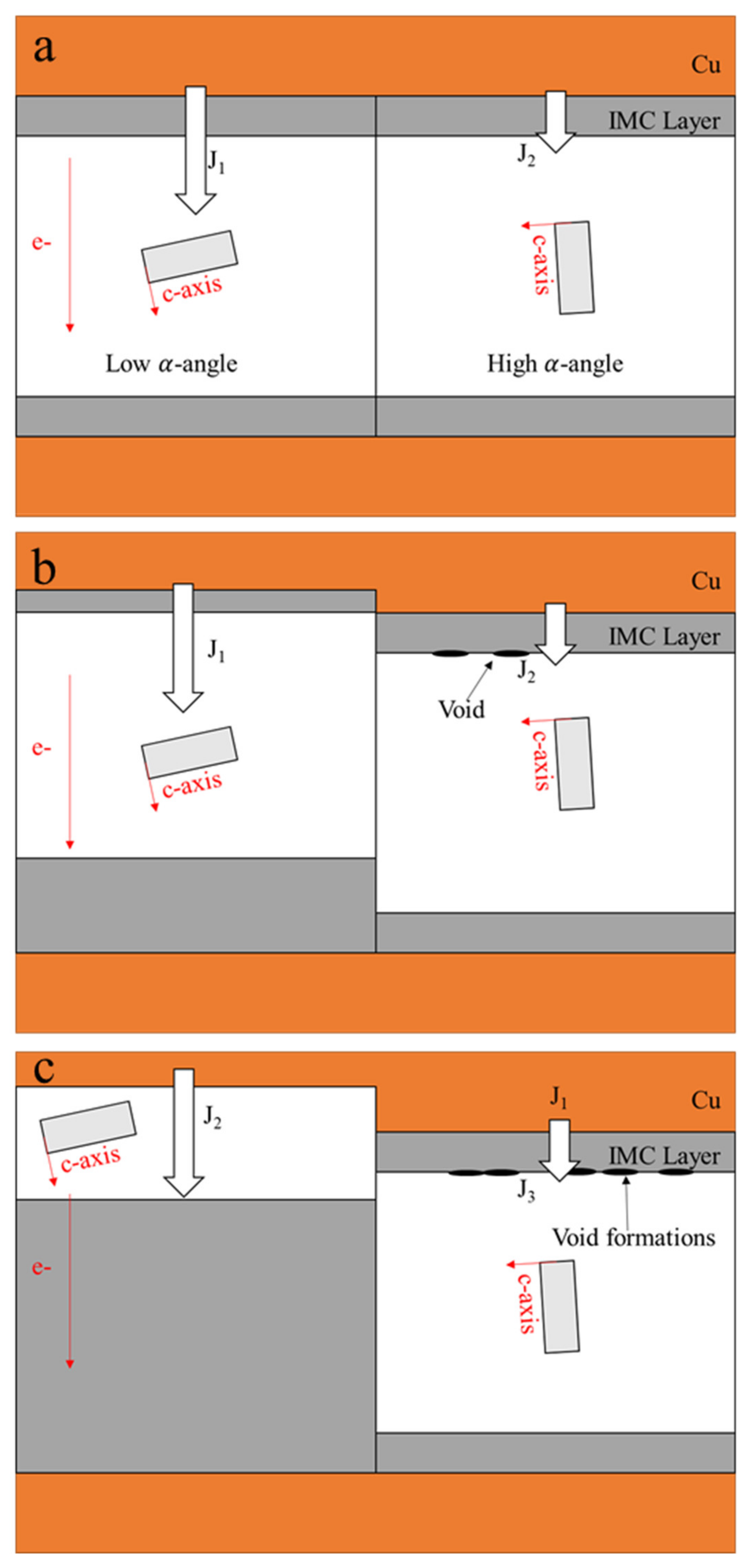
Figure 1. A schematic of the different failure modes induced by the grain orientation in solder joints: (a) initial stage; (b) intermediate duration; (c) terminal stage.
However, the void formations and UBM dissolutions at the cathode of the high α-angle grain might be influenced by current crowding during electromigration [61][62][63][64]. Line-type solder joints were fabricated to avoid the complication of current crowding, providing a purer surrounding to observe the effect of the Sn grain orientation on the electromigration in Sn-rich solder joints [65][66][67][68]. UBM dissolution dominated by the Sn grain orientation was observed in the line-type solder joint, without the current crowding effect [68]. As current crowding played no role in the line-type solder joints, there were no obvious void formations at the cathode of the high α-angle grain after EM at a 104 A cm−2 current density for 400 h. An EBSD orientation map is shown for the c-axis direction in the line-type solder joint. Interestingly, the formation of the Sn-Ni IMC at the anode and the dissolution of the Ni substrate at the cathode occur along with the angles of the c-axis of Sn grains. The detailed mechanism behind this has been proven in [69]. The components of the electron field (E→), Sn unit cell, and the atomic flux (J→) during EM. There is an φ-angle between the E→ and J→ and an α-angle between the c-axis and E→. The φ-angle can be calculated by [70]:
where Da and Dc are the diffusivity levels, respectively, along a-axis and c-axis in different materials. If the α-angles are 28.61° and 58.57°, the φ-angles will be 28.28° and 57.66°, respectively. The angles are nearly identical to each other. Additionally, the atomic flux J→ can be expressed as [70]:
The atomic flux along the electron field (JE) can be expressed as:
As mentioned above, when the α-angle is very low, the atomic flux deviation from the c-axis will become largely considerable. Consequently, the atoms of the UBM mainly migrate along the c-axis from the cathode to the anode through the interstitial diffusion because the contribution of Dasin2α is low and Dc ≫ Da. In a high α-angle grain, the JE is very low because (Dasin2α+Dccos2α) is very small, and even ≅Dasin2α could be neglected in the comparison with a low α-angle grain. Meanwhile, the atomic flux deviation from the c-axis is very limited, and the UBM dissolution and IMC formation seldom occur along the c-axis. Similar results in the solder joints with Cu UBMs were also observed in [71][72][73]. Moreover, in the Sn-Pb solder microbump, when the electromigration test was carried out at −196 °C, the anisotropic migration of the Pb did not occur. Instead, their study found that the Pb migrated in a parallel path. On the contrary, the Pb rapidly migrated along a specific direction (the c-axis of the Sn) during the electromigration at room temperature [74]. The different migration routes of the Pb were due to the different crystal structures of the Sn at the two temperatures. At <13 °C, the Sn type was α-Sn with a face-centered cubic structure [75], so the electric properties of α-Sn were isotropic. At room temperature, the Sn type was β-Sn with a body-centered tetragonal structure, which was anisotropic [76]. The results exhibit the significant effect of the β-Sn grain orientation on the electromigration in solder microbumps. Therefore, the electromigration along the Sn c-axis is clearly explained.
Although the effect of the Sn c-axis on the electromigration is known. This phenomenon would be more significant with the increase in the misorientation angles of the grain boundaries. However, due to the considerable number of Sn cyclic-twin boundaries, which are a type of coherent boundary in β-Sn crystals [77], in Sn-Ag [78] the atoms rarely diffuse along the cycling twining boundary (CTB) compared to the boundaries with high misorientation angles. In other words, the effects of grain boundaries on electromigration would be dependent on the type of grain boundary. If there is no CTB in a Sn-rich solder, the UBM dissolutions and IMC formations are influenced by the grain boundary misorientation angles rather than the Sn grain orientations [79]. This is why the EM damages were retarded by the CTB [49][78].
This entry is adapted from the peer-reviewed paper 10.3390/ma15145086
References
- Abtew, M.; Selvaduray, G. Lead-Free Solders in Microelectronics. Mater. Sci. Eng. R Rep. 2000, 27, 95–141.
- Suganuma, K. Advances in Lead-Free Electronics Soldering. Curr. Opin. Solid State Mater. Sci. 2001, 5, 55–64.
- Subramanian, K.N. (Ed.) Preface; John Wiley and Sons, Ltd.: Chichester, UK, 2012; ISBN 9780470971826.
- Morris, J.W.; Goldstein, J.L.F.; Mei, Z. Microstructure and Mechanical Properties of Sn-In and Sn-Bi Solders. JOM 1993, 45, 25–27.
- Yang, W.; Messler, R.W.; Felton, L.E. Microstructure Evolution of Eutectic Sn-Ag Solder Joints. J. Electron. Mater. 1994, 23, 765–772.
- Lee, B.-J.; Oh, C.-S.; Shim, J.-H. Thermodynamic Assessments of the Sn-In and Sn-Bi Binary Systems. J. Electron. Mater. 1996, 25, 983–991.
- Kim, K.S.; Huh, S.H.; Suganuma, K. Effects of Intermetallic Compounds on Properties of Sn–Ag–Cu Lead-Free Soldered Joints. J. Alloys Compd. 2003, 352, 226–236.
- Gao, H.; Wei, F.; Sui, Y.; Qi, J. Growth Behaviors of Intermetallic Compounds on the Sn-0.7Cu-10Bi-XCo/Co Interface during Multiple Reflow. Mater. Des. 2019, 174, 107794.
- Kolenak, R.; Kostolný, I.; Sahul, M. Direct Bonding of Silicon with Solders Type Sn-Ag-Ti. Solder. Surf. Mt. Technol. 2016, 28, 149–158.
- Hou, Z.; Zhao, X.; Gu, Y.; Tan, C.; Huo, Y.; Li, H.; Shi, S.; Liu, Y. Enhancement Mechanism of Te Doping on Microstructure, Wettability and Mechanical Properties of Sn–Bi-Based Solder. Mater. Sci. Eng. A 2022, 848, 143445.
- Korhonen, T.-M.; Kivilahti, J.K. Thermodynamics of the Sn-In-Ag Solder System. J. Electron. Mater. 1998, 27, 149–158.
- Alam, M.O.; Chan, Y.C.; Tu, K.N. Effect of 0.5 Wt% Cu Addition in Sn–3.5%Ag Solder on the Dissolution Rate of Cu Metallization. J. Appl. Phys. 2003, 94, 7904.
- Seo, S.-K.; Kang, S.K.; Shih, D.-Y.; Lee, H.M. An Investigation of Microstructure and Microhardness of Sn-Cu and Sn-Ag Solders as Functions of Alloy Composition and Cooling Rate. J. Electron. Mater. 2009, 38, 257–265.
- Wu, C.M.L.; Yu, D.Q.; Law, C.M.T.; Wang, L. Properties of Lead-Free Solder Alloys with Rare Earth Element Additions. Mater. Sci. Eng. R Rep. 2004, 44, 1–44.
- Shen, Y.-A.; Chen, H.-Z.; Chen, S.-W.; Chiu, S.-K.; Guo, X.-Y.; Hsieh, Y.-P. Graphene as a Diffusion Barrier at the Interface of Liquid–State Low-Melting Sn–58Bi Alloy and Copper Foil. Appl. Surf. Sci. 2022, 578, 152108.
- Frear, D.R.; Jang, J.W.; Lin, J.K.; Zhang, C. Pb-Free Solders for Flip-Chip Interconnects. JOM 2001, 53, 28–33.
- Zeng, K.; Tu, K.N. Six Cases of Reliability Study of Pb-Free Solder Joints in Electronic Packaging Technology. Mater. Sci. Eng. R Rep. 2002, 38, 55–105.
- Shen, Y.-A.; Chen, S.-W.; Chen, H.-Z.; Chang, C.-M.; Ouyang, Y.-H. Extremely Thin Interlayer of Multi-Element Intermetallic Compound between Sn-Based Solders and FeCoNiMn High-Entropy Alloy. Appl. Surf. Sci. 2021, 558, 149945.
- Tu, K.N. Recent Advances on Electromigration in Very-Large-Scale-Integration of Interconnects. J. Appl. Phys. 2003, 94, 5451–5473.
- Meinshausen, L.; Weide-Zaage, K.; Frémont, H. Dynamical IMC-Growth Calculation. Microelectron. Reliab. 2015, 55, 1832–1837.
- Chan, H.T.; Lin, C.F.; Yen, Y.W.; Chen, C.M. Effects of Current Stressing on the P-Bi2Te3/Sn Interfacial Reactions. J. Alloys Compd. 2016, 668, 91–96.
- Chen, C.; Tong, H.M.; Tu, K.N. Electromigration and Thermomigration in Pb-Free Flip-Chip Solder Joints. Annu. Rev. Mater. Res. 2010, 40, 531–555.
- Huang, M.L.; Zhang, Z.J.; Zhao, N.; Zhou, Q. A Synchrotron Radiation Real-Time in Situ Imaging Study on the Reverse Polarity Effect in Cu/Sn–9Zn/Cu Interconnect during Liquid–Solid Electromigration. Scr. Mater. 2013, 68, 853–856.
- Chen, C.M.; Chen, S.W. Electromigration Effect upon the Sn/Ag and Sn/Ni Interfacial Reactions at Various Temperatures. Acta Mater. 2002, 50, 2461–2469.
- Bashir, M.N.; Haseeb, A.S.M.A. Grain Size Stability of Interfacial Intermetallic Compound in Ni and Co Nanoparticle-Doped SAC305 Solder Joints under Electromigration. J. Mater. Sci. Mater. Electron. 2022, 33, 14240–14248.
- Lin, Y.H.; Tsai, C.M.; Hu, Y.C.; Lin, Y.L.; Kao, C.R. Electromigration-Induced Failure in Flip-Chip Solder Joints. J. Electron. Mater. 2005, 34, 27–33.
- Abdulhamid, M.F.; Basaran, C. Influence of Thermomigration on Lead-Free Solder Joint Mechanical Properties. J. Electron. Packag. 2009, 131, 011002.
- Chen, C.; Hsiao, H.-Y.; Chang, Y.-W.; Ouyang, F.; Tu, K.N. Thermomigration in Solder Joints. Mater. Sci. Eng. R Rep. 2012, 73, 85–100.
- Park, S.; Dhakal, R.; Lehman, L.; Cotts, E. Measurement of Deformations in SnAgCu Solder Interconnects under in Situ Thermal Loading. Acta Mater. 2007, 55, 3253–3260.
- Matin, M.A.; Vellinga, W.P.; Geers, M.G.D. Thermomechanical Fatigue Damage Evolution in SAC Solder Joints. Mater. Sci. Eng. A 2007, 445–446, 73–85.
- Ahat, S.; Sheng, M.; Luo, L. Effects of Static Thermal Aging and Thermal Cycling on the Microstructure and Shear Strength of Sn95.5Ag3.8Cu0.7 Solder Joints. J. Mater. Res. 2001, 16, 2914–2921.
- Pearson, W.B. (Ed.) A Handbook of Lattice Spacings and Structures of Metals and Alloys; Elsevier: London, UK, 1958; ISBN 9781483213187.
- Dyson, B.F.; Anthony, T.R.; Turnbull, D. Interstitial Diffusion of Copper in Tin. J. Appl. Phys. 1967, 38, 3408.
- Yeh, D.C.; Huntington, H.B. Extreme Fast-Diffusion System: Nickel in Single-Crystal Tin. Phys. Rev. Lett. 1984, 53, 1469–1472.
- Rayne, J.A.; Chandrasekhar, B.S. Elastic Constants of β Tin from 4.2 °K to 300 °K. Phys. Rev. 1960, 120, 1658–1663.
- Deshpande, V.T.; Sirdeshmukh, D.B. IUCr Thermal Expansion of Tin in the β–γ Transition Region. Acta Crystallogr. 1962, 15, 294–295.
- Case, S.K.; Gueths, J.E. Anisotropy of the Temperature-Dependent Resistivity of Tin between 8 and 300 °K. Phys. Rev. B 1970, 2, 3843–3848.
- Lee, B.-Z.; Lee, D.N. Spontaneous Growth Mechanism of Tin Whiskers. Acta Mater. 1998, 46, 3701–3714.
- Ernst, B.; Keim, S.; Tetzlaff, U. On the Anisotropic Indentation Modulus and Anisotropic Creep Behavior of β-Sn Characterized by Nanoindentation Methods. Mater. Sci. Eng. A 2022, 848, 143392.
- Tu, K.N. Reliability Challenges in 3D IC Packaging Technology. Microelectron. Reliab. 2011, 51, 517–523.
- Chen, K.-N.; Tu, K.-N. Materials Challenges in Three-Dimensional Integrated Circuits. MRS Bull. 2015, 40, 219–222.
- Huang, Y.T.; Hsu, H.H.; Wu, A.T. Electromigration-Induced Back Stress in Critical Solder Length for Three-Dimensional Integrated Circuits. J. Appl. Phys. 2014, 115, 034904.
- Black, J.R. Electromigration Failure Modes in Aluminum Metallization for Semiconductor Devices. Proc. IEEE 1969, 57, 1587–1594.
- Black, J.R. Electromigration—A Brief Survey and Some Recent Results. IEEE Trans. Electron Devices 1969, 16, 338–347.
- Ho, P.S.; Kwok, T. Electromigration in Metals. Rep. Prog. Phys. 1989, 52, 301–348.
- Lee, P.T.; Hsieh, W.Z.; Lee, C.Y.; Tseng, S.C.; Tang, M.T.; Chiang, C.Y.; Kao, C.R.; Ho, C.E. Synchrotron X-ray Study of Electromigration, Whisker Growth, and Residual Strain Evolution in a Sn Blech Structure. Scr. Mater. 2022, 214, 114682.
- Jepiti, P.; Yoon, S.; Kim, J. Electromigration Reliability in Ag Lines Printed with Nanoparticle Inks: Implications for Printed Electronics. ACS Appl. Nano Mater. 2022, 5, 2569–2577.
- Liu, Y.C.; Yu, Y.S.; Lin, S.K.; Chiu, S.J. Electromigration Effect upon Single- and Two-Phase Ag-Cu Alloy Strips: An In Situ Study. Scr. Mater. 2019, 173, 134–138.
- Lu, M.; Shih, D.-Y.; Lauro, P.; Goldsmith, C.; Henderson, D.W. Effect of Sn Grain Orientation on Electromigration Degradation Mechanism in High Sn-Based Pb-Free Solders. Appl. Phys. Lett. 2008, 92, 211909.
- Wang, Y.; Lu, K.H.; Gupta, V.; Stiborek, L.; Shirley, D.; Im, J.; Ho, P.S. Effect of Sn Grain Structure on Electromigration Reliability of Pb-Free Solders. In Proceedings of the 2011 IEEE 61st Electronic Components and Technology Conference (ECTC), Lake Buena Vista, FL, USA, 31 May–3 June 2011; pp. 711–716.
- Lee, K.; Kim, K.-S.; Tsukada, Y.; Suganuma, K.; Yamanaka, K.; Kuritani, S.; Ueshima, M. Effects of the Crystallographic Orientation of Sn on the Electromigration of Cu/Sn–Ag–Cu/Cu Ball Joints. J. Mater. Res. 2011, 26, 467–474.
- Wang, Y.; Lu, K.H.; Gupta, V.; Stiborek, L.; Shirley, D.; Chae, S.-H.; Im, J.; Ho, P.S. Effects of Sn Grain Structure on the Electromigration of Sn–Ag Solder Joints. J. Mater. Res. 2012, 27, 1131–1141.
- Wei, C.C.; Yu, C.H.; Tung, C.H.; Huang, R.Y.; Hsieh, C.C.; Chiu, C.C.; Hsiao, H.Y.; Chang, Y.W.; Lin, C.K.; Liang, Y.C.; et al. Comparison of the Electromigration Behaviors between Micro-Bumps and C4 Solder Bumps. In Proceedings of the Proceedings—Electronic Components and Technology Conference, Lake Buena Vista, FL, USA, 31 May–3 June 2011; pp. 706–710.
- Huang, M.L.; Zhao, J.F.; Zhang, Z.J.; Zhao, N. Role of Diffusion Anisotropy in β-Sn in Microstructural Evolution of Sn-3.0Ag-0.5Cu Flip Chip Bumps Undergoing Electromigration. Acta Mater. 2015, 100, 98–106.
- Lin, C.F.; Lee, S.H.; Chen, C.M. Effect of Sn Grain Orientation on the Cu6Sn5 Formation in a Sn-Based Solder Under Current Stressing. Metall. Mater. Trans. A 2012, 43, 2571–2573.
- Liu, C.Y.; Chen, C.; Mal, A.K.; Tu, K.N. Direct Correlation between Mechanical Failure and Metallurgical Reaction in Flip Chip Solder Joints. J. Appl. Phys. 1999, 85, 3882–3886.
- Jang, J.W.; De Silva, A.P.; Lee, T.Y.; Lin, J.K.; Frear, D.R. Direct Correlation between Microstructure and Mechanical Tensile Properties in Pb-Free Solders and Eutectic SnPb Solder for Flip Chip Technology. Appl. Phys. Lett. 2001, 79, 482–484.
- Ren, F.; Nah, J.-W.; Tu, K.N.; Xiong, B.; Xu, L.; Pang, J.H.L. Electromigration Induced Ductile-to-Brittle Transition in Lead-Free Solder Joints. Appl. Phys. Lett. 2006, 89, 141914.
- Zhang, L.; Wang, Z.G.; Shang, J.K. Current-Induced Weakening of Sn3.5Ag0.7Cu Pb-Free Solder Joints. Scr. Mater. 2007, 56, 381–384.
- Bashir, M.N.; Haseeb, A.S.M.A.; Rahman, A.Z.M.S.; Fazal, M.A.; Kao, C.R. Reduction of Electromigration Damage in SAC305 Solder Joints by Adding Ni Nanoparticles through Flux Doping. J. Mater. Sci. 2015, 50, 6748–6756.
- Yeh, E.C.C.; Choi, W.J.; Tu, K.N.; Elenius, P.; Balkan, H. Current-Crowding-Induced Electromigration Failure in Flip Chip Solder Joints. Appl. Phys. Lett. 2002, 80, 580–582.
- Chang, Y.-W.; Cheng, Y.; Xu, F.; Helfen, L.; Tian, T.; Di Michiel, M.; Chen, C.; Tu, K.-N.; Baumbach, T. Study of Electromigration-Induced Formation of Discrete Voids in Flip-Chip Solder Joints by in-Situ 3D Laminography Observation and Finite-Element Modeling. Acta Mater. 2016, 117, 100–110.
- Ahmed, M.T.; Motalab, M.; Suhling, J.C. Impact of Mechanical Property Degradation and Intermetallic Compound Formation on Electromigration-Oriented Failure of a Flip-Chip Solder Joint. J. Electron. Mater. 2020, 50, 233–248.
- Jeong, H.; Lee, C.J.; Kim, J.H.; Son, J.Y.; Jung, S.B. Electromigration Behavior of Cu Core Solder Joints Under High Current Density. Electron. Mater. Lett. 2020, 16, 513–519.
- Lee, K.; Kim, K.-S.; Suganuma, K. Influence of Indium Addition on Electromigration Behavior of Solder Joint. J. Mater. Res. 2011, 26, 2624–2631.
- Ke, J.H.; Chuang, H.Y.; Shih, W.L.; Kao, C.R. Mechanism for Serrated Cathode Dissolution in Cu/Sn/Cu Interconnect under Electron Current Stressing. Acta Mater. 2012, 60, 2082–2090.
- Huang, T.C.; Yang, T.L.; Ke, J.H.; Li, C.C.; Kao, C.R. Precipitation Induced by Diffusivity Anisotropy in Sn Grains under Electron Current Stressing. J. Alloys Compd. 2013, 555, 237–240.
- Huang, T.C.; Yang, T.L.; Ke, J.H.; Hsueh, C.H.; Kao, C.R. Effects of Sn Grain Orientation on Substrate Dissolution and Intermetallic Precipitation in Solder Joints under Electron Current Stressing. Scr. Mater. 2014, 80, 37–40.
- Chen, J.-Q.; Liu, K.-L.; Guo, J.-D.; Ma, H.-C.; Wei, S.; Shang, J.-K. Electromigration Anisotropy Introduced by Tin Orientation in Solder Joints. J. Alloys Compd. 2017, 703, 264–271.
- Chen, J.-Q.; Guo, J.-D.; Liu, K.-L.; Shang, J.-K. Dependence of Electromigration Damage on Sn Grain Orientation in Sn–Ag–Cu Solder Joints. J. Appl. Phys. 2013, 114, 153509.
- Wang, Y.; Wang, Y.; Ma, L.; Han, J.; Guo, F. IMC Growth Behavior along C-Axis of Sn Grain under Current Stressing. J. Mater. Sci. Mater. Electron. 2019, 29, 13180–13187.
- Wang, Y.; Wang, Y.; Han, J.; Tan, S.; Guo, F. Effects of Sn Grain C-Axis on Electromigration in Cu Reinforced Composite Solder Joints. J. Mater. Sci. Mater. Electron. 2018, 29, 5954–5960.
- Xu, K.; Fu, X.; Wang, X.; Fu, Z.; Yang, X.; Chen, S.; Shi, Y.; Huang, Y.; Chen, H. The Effect of Grain Orientation of β-Sn on Copper Pillar Solder Joints during Electromigration. Materials 2021, 15, 108.
- Fu, X.; En, Y.; Zhou, B.; Chen, S.; Huang, Y.; He, X.; Chen, H.; Yao, R. Microstructure and Grain Orientation Evolution in SnPb/SnAgCu Interconnects Under Electrical Current Stressing at Cryogenic Temperature. Materials 2019, 12, 1593.
- Groves, S.; Paul, W. Band Structure of Gray Tin. Phys. Rev. Lett. 1963, 11, 194.
- Vincent, S.; Kleiven, D.; Lastra, J.M.G.; Chang, J.H. Thermodynamic Investigation of Phase Transformation in Sn Anode for Magnesium Batteries. APL Mater. 2022, 10, 071104.
- Lehman, L.P.; Xing, Y.; Bieler, T.R.; Cotts, E.J. Cyclic Twin Nucleation in Tin-Based Solder Alloys. Acta Mater. 2010, 58, 3546–3556.
- Shen, Y.-A.; Chen, C. Effect of Sn Grain Orientation on Formation of Cu6Sn5 Intermetallic Compounds during Electromigration. Scr. Mater. 2017, 128, 6–9.
- Tasooji, A.; Lara, L.; Lee, K. Effect of Grain Boundary Misorientation on Electromigration in Lead-Free Solder Joints. J. Electron. Mater. 2014, 43, 4386–4394.
This entry is offline, you can click here to edit this entry!