Sn-rich solder joints in three-dimensional integrated circuits and their reliability issues, such as electromigration (EM), thermomigration (TM), and thermomechanical fatigue (TMF), have drawn attention related to their use in electronic packaging. The Sn grain orientation is important in reliability issues due to its anisotropic diffusivity. This study reviews the effects of the Sn grain orientation on the EM in Sn-rich solder joints. The findings indicate that in spite of the failure modes dominated by the Sn grain orientation, the size and shape of the solder joint, as well as the Sn microstructures, such as the cycling twining boundary (CTB), single crystals, and misorientations of the Sn grain boundary, should be considered in more detail.
1. Introduction
Lead-free solder has been widely used in electronic packaging since the restriction of the inclusion of lead in consumer electronics [
1,
2,
3]. Lead-free solders are Sn-based alloys with various kinds of element additions, including Ag, Cu, Ni, Bi, Zn, Ti, In, and graphene [
4,
5,
6,
7,
8,
9,
10]. Such alloys possess a wide range of melting points, electrical and mechanical properties, microstructures, and wetting behaviors for various applications in electronic devices [
11,
12,
13,
14,
15]. Among them, Sn-rich solder, which contains considerable amounts of Sn in the solder matrixes, is widely adopted in solder joints that are assembled via under-bump metallization (UBM), using a solder alloy and intermetallic compound (IMC) at the interface between the solder and the UBM method via a reflow process at a suitable temperature [
16,
17,
18]. The reliability issues of Sn-rich solder joints have drawn substantial concerns, the first of which is the EM reliability during a consistent electron flow with a critical current density in Sn-rich solder joints [
19,
20,
21], inducing UBM dissolution, rapid IMC growth, void formation, and severe Joule heating [
22,
23,
24,
25]. Then, the Joule heating induces a temperature gradient in the solder joint, known as the TM [
22,
26,
27,
28]. Additionally, during multiple cycles of increases and decreases in the internal temperature, i.e., thermal cycling tests, the TMF is another important reliability issue because of the CTE mismatches between the Sn grains, Si chip and polymer substrate, Sn-rich solder and Si chip, and Sn-rich solder and polymer substrate [
29,
30,
31]. However, the properties of Sn-rich solders are dominated by β-Sn crystals, and the effects of their properties on the EM, TM, and TMF of Sn-rich solder joints are worth investigating in detail.
Sn possesses a body-centered tetragonal structure (a-axis: 0.583
Å, c-axis: 0.318
Å at 25 °C) [
32], inducing anisotropic diffusion and thermal, mechanical, and electrical properties [
33,
34,
35,
36,
37,
38,
39]. The effects of these anisotropic properties on the EM, TM, and TMF reliability levels of solder joints are critical issues that have been deeply studied by many researchers. Moreover, due to the miniaturization and high performance of electronic devices, three-dimensional integrated circuits (3DICs) have become very popular and critical for the next generation of electronic packaging [
40,
41,
42]. The use of a microbump is particularly important to connect the through-silicon-via (TSV) and chip in 3DICs. However, with the reduction in solder volume, the Sn-rich solder in the microbumps may contain few Sn grains or even a single-crystal-like structure. The effects of the Sn grain orientation on these issues are more significant than in flip–chip solder joints because of the dominant grains in the microbumps.
2. Effect of Sn Grain Orientation on Electromigration
Electromigration is the phenomenon whereby atomic migration is caused by the momentum transfer between electrons and diffusing specimens under an electric current [
43,
44,
45,
46,
47,
48]. The atomic flux diffusing during electromigration can be expressed as [
19]:
where
C is the atomic concentration,
D is the diffusivity,
Z* is the effective charge number,
K is Boltzmann constant,
T is the absolute temperature,
e is the electron charge,
E is the electron field,
ρ is the resistivity, and
j is the current density. Because interstitial diffusion dominates the electromigration behavior of Sn-rich solder joints, as the Sn self-diffusion rate is very low [
33], the considerable atoms of UBMs would migrate in Sn solder from the cathode to the anode. Meanwhile, the anisotropic diffusion of Sn grains induces different failure modes due to the different atomic fluxes.
Table 1 summarizes the diffusivity levels of Cu and Ni along the c-axis and a-axis during EM in Sn at 120 °C. The diffusivity rate of Cu along the c-axis of Sn is approximately 61 times larger than that along the a-axis. For Ni, the diffusivity rate along the c-axis is approximately 70,000 times larger than that along the a-axis, being much greater. Therefore, the effect of the Sn grain orientation on EM failure in Sn solder joints with Ni UBMs under a current density of 7.7 × 10
3 A/cm
2 was first observed by Lu et al. [
49]. Since then, substantial studies on this effect have been reported [
50,
51,
52,
53,
54,
55]. In the studies, the extra-fast UBM dissolution of Cu/Ni at the cathode occurs as the electron flow is closely parallel to the c-axis, which possesses a high diffusion rate. However, when the electron flow is vertical to the c-axis, i.e., closely parallel to the a-axis of Sn, void formations can be observed instead of the depletion of UBM. The UBM dissolutions and void formations rapidly increase the resistivity of the solder joints, which is a critical reliability issue. On the other hand, on the anode side, considerable IMC growth can be observed when the electron flow is parallel to the c-axis of Sn. In many studies, in addition to increasing the resistivity, the growth of brittle IMC induced poor mechanical reliability in Sn-rich solder joints [
56,
57,
58,
59,
60]. Therefore, the mechanism of the effect of the Sn grain orientation on the electromigration is very important.
Table 1. The diffusivity levels of Cu and Ni calculated at 120 °C.
| Type of Diffusion |
Diffusivity (cm2/s) |
Condition |
Ref. |
| DCu in Sn |
5.96 × 10⁻⁶ |
Along c-axis |
[36] |
| |
9.7 × 10⁻⁸ |
Along a-axis |
[36] |
| DNi in Sn |
8.22 × 10⁻⁵ |
Along c-axis |
[37] |
| |
1.10 × 10⁻⁹ |
Along a-axis |
[37] |
In this section, the α-angle is defined as the angle between the c-axis of Sn and the electron flow. The diffusivity of Sn grains in Cu can be expressed as [
34]:
where the diffusivity levels along the c-axis (
Dc,Cu) and a-axis (
Da,Cu) can be expressed as [
33]:
where
R is the universal gas constant and
T is the absolute temperature. The temperatures directly affect the diffusivity levels, and a higher temperature induces a higher atomic flux during the diffusion, accelerating the occurrence of the IMC growth and UBM dissolution. Hence, when the Sn solder has a low α-angle grain, a considerable amount of atoms from the dissolution of UBMs at the cathode diffuse to the anode. Conversely, instead of fast interstitial diffusion along a low α-angle grain, the Sn self-diffusion dominates the EM, inducing void formations and a little UBM dissolution at the cathode.
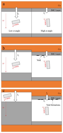
Figure 2a shows a Cu/Sn-rich solder–Cu joint with high and low α-angle grains of Sn. J
1 and J
2 are the Cu fluxes via a low and high α-angle grain, respectively. Owing to J
1 >> J
2, the IMC decomposition caused by the fast interstitial diffusion along the low α-angle grain is rapid at the cathode, while void formation occurs in the high α-angle grain, as shown in
Figure 2b. With the passing of time (
Figure 2c), in the low α-angle grain, serious UBM dissolution at the cathode after the complete decomposition of as-bonded IMC and the substantial IMC growth at the anode are observed; conversely, in the high α-angle grain, there is no significant change in IMC thickness due to the very low J
2 and the greater number of void formations at the cathode.
Figure 2. A schematic of the different failure modes induced by the grain orientation in solder joints: (a) initial stage; (b) intermediate duration; (c) terminal stage.
However, the void formations and UBM dissolutions at the cathode of the high α-angle grain might be influenced by current crowding during electromigration [
62,
63,
64,
65]. Line-type solder joints were fabricated to avoid the complication of current crowding, providing a purer surrounding to observe the effect of the Sn grain orientation on the electromigration in Sn-rich solder joints [
66,
67,
68,
69]. UBM dissolution dominated by the Sn grain orientation was observed in the line-type solder joint, without the current crowding effect [
69]. As current crowding played no role in the line-type solder joints, there were no obvious void formations at the cathode of the high α-angle grain after EM at a 10
4 A cm
−2 current density for 400 h. An EBSD orientation map is shown for the c-axis direction in the line-type solder joint. Interestingly, the formation of the Sn-Ni IMC at the anode and the dissolution of the Ni substrate at the cathode occur along with the angles of the c-axis of Sn grains. The detailed mechanism behind this has been proven in [
70]. The components of the electron field (
E→), Sn unit cell, and the atomic flux (
J→) during EM. There is an
φ-angle between the
E→ and
J→ and an
α-angle between the c-axis and
E→. The
φ-angle can be calculated by [
71]:
where
Da and
Dc are the diffusivity levels, respectively, along a-axis and c-axis in different materials. If the
α-angles are 28.61° and 58.57°, the
φ-angles will be 28.28° and 57.66°, respectively. The angles are nearly identical to each other. Additionally, the atomic flux
J→ can be expressed as [
71]:
The atomic flux along the electron field (JE) can be expressed as:
As mentioned above, when the
α-angle is very low, the atomic flux deviation from the c-axis will become largely considerable. Consequently, the atoms of the UBM mainly migrate along the c-axis from the cathode to the anode through the interstitial diffusion because the contribution of
Dasin2α is low and
Dc ≫ Da. In a high
α-angle grain, the
JE is very low because
(Dasin2α+Dccos2α) is very small, and even
≅Dasin2α could be neglected in the comparison with a low
α-angle grain. Meanwhile, the atomic flux deviation from the c-axis is very limited, and the UBM dissolution and IMC formation seldom occur along the c-axis. Similar results in the solder joints with Cu UBMs were also observed in [
72,
73,
74]. Moreover, in the Sn-Pb solder microbump, when the electromigration test was carried out at −196 °C, the anisotropic migration of the Pb did not occur. Instead, the study found that the Pb migrated in a parallel path. On the contrary, the Pb rapidly migrated along a specific direction (the c-axis of the Sn) during the electromigration at room temperature [
75]. The different migration routes of the Pb were due to the different crystal structures of the Sn at the two temperatures. At <13 °C, the Sn type was α-Sn with a face-centered cubic structure [
76], so the electric properties of α-Sn were isotropic. At room temperature, the Sn type was β-Sn with a body-centered tetragonal structure, which was anisotropic [
77]. The results exhibit the significant effect of the β-Sn grain orientation on the electromigration in solder microbumps. Therefore, the electromigration along the Sn c-axis is clearly explained.
Although the effect of the Sn c-axis on the electromigration is known. This phenomenon would be more significant with the increase in the misorientation angles of the grain boundaries. However, due to the considerable number of Sn cyclic-twin boundaries, which are a type of coherent boundary in
β-Sn crystals [
80], in Sn-Ag [
61] the atoms rarely diffuse along the CTB compared to the boundaries with high misorientation angles. In other words, the effects of grain boundaries on electromigration would be dependent on the type of grain boundary. If there is no CTB in a Sn-rich solder, the UBM dissolutions and IMC formations are influenced by the grain boundary misorientation angles rather than the Sn grain orientations [
78]. This is why the EM damages were retarded by the CTB [
49,
61].
This entry is adapted from the peer-reviewed paper 10.3390/ma15145086